Note: Descriptions are shown in the official language in which they were submitted.
CA 02240679 1998-06-16
W O 97/~4802 PCTrUS96/20326
IMPULSE NOISE EFFl~CT REDUCTION
~ This invention relates to data commllnir~*r,n systems and, in
parlicular, to a lec~iver sy~eLu in which the effect of noise impulses (e.g.,
5 noise spikes) is rellnre-l
The o~;u~ ce and presence at the input of a l~;~iv~r of u~w~ted
noise impulses ~e.g., noise spikes) having .q~ fic~ntly greater ~mplihl(le (and
energy) than the desired data .qi~n~l~ h~ei~g t~n~mitted presents numerous
prohlemc;
Known l~~iv~r systems inrlnrl~ adaptive eqll~li7Prc such as a
ic~n feedback equalizer ~DFE) for compPnq~*ng for noise and distortion
introduced in the ~ncmiq.qinn rh~nnPl b~w~ a trsm~ - and its
~t:ivel. A D~: may typically inrlll~P an adaptive feed-rol vv~d filter and an
adaptive fee~h~rk filter. A noise impulse (e.g., an ullwalll,ed noise spike)
15 produces a cignifir~nt problem in t_e adjllQ~nPnt of the coPffiriPntq of the
adaptive filters of a DE~E. Typically, a noise impulse can occur either during
the "I ,.;..;..~' phase of the D~E or dw~ng the data t~nqmiqqion (steady-
state) phase of the DE E. The problem due to a noise impulse is more acute
dllring ~-,.;..;..g because the adaptive filters are norm~lly adjusted using
20 larger steps during that phase. How~v~l, the problem is always present.
Dnring the data trz~nqmi~inn phase, the D~E is also prone to "error
prop~ti~ n" because a slicer c~cuit in the D~E makes a rl~iqion i.e., an
e~im~t~, as to the correct data symbol. Since the DPE ll*li7~ feedback, an
incorrect c~im~te as to the current l~iv~d symbol affects subsequent
2 5 lect iv~d symbols. The net effect of a noise impulse is to cause the coPffir~i~nt-q
of the adaptive filters to be misadjusted (i.e., i~ erly and incoll~;lly
CA 02240679 1998-06-16
W O 97/24802 PCTrUS96/20326
adjusted) which, in tu~, causes the adaptive filters to propagate erroneous
infnrm~t.~?n
In full duplex systems there is also inrlll(lP-l echo r~n~PlPr ~
between the ~n~ il(e.- and the l.~c~ivel. Typically, an echo r~nr~pler is
5 cnnnertefl between the tr~n.~ ~R) section and the ~ ~v~r ~REC)
section. I'he echo r~nrPlPr is an adaptive transversal filter that adaptively
learns the response of the hybrid, and gPn~r,ltP.q a replica of 1~hat response
which is subLl~ed from the hyb~d output to yield an echo-free lec~ived
signal. Clearly, any large noise ~mpulse injected into the l~~iv~ line during
10 the ~ and/or du~ing data trzln.cmi~ ion of the echo r~nrPl~pr cu~ the
response of the c~ncf~l~r for an P.X~nllP~ period of time. The net effect of a
naise impulse is to cause the coPffiriPn~ of the echo c~ncPlin~ filter to be
isadjusted ~i.e., i~ .J~erly and inc~ ;Lly adjusted) which, in turn, causes
the adaptive filters to propagate Prrnneous infortnzl*nn
In the case of the echo ~ncPl~r filter and the adaptive eq~ Pr, a
large noise ~mpulse causes the prop~F~*on of errors within their respective
filters. Huw~ver, the error levels decrease over time due to the adaptive
nature of the filters.
Tr~n.~ receiver systems also include certain precoding filters
20 such as the tnmlin.~nn preco~ling, which are "set" (e.g, their filter coPffir~iPnt~
are updated and adjusted by a DP~E.) during certain phases (i.e., during
training or immediately thereafter). Once "set", these filters remain set
throughout a subsequent data t~nsmi~.qion phase. Obviously, iî a noise
impulse is injected in the system du~ing the ~z~inin~ of such filters, the filter
25 will be ~~ erly set throughout the subsequent data t~n.~mi.c.~ion phase
and the ~n~mit~ed data will cont~in a high degree of noise and errors.
CA 02240679 1998-06-16
W O 97/24802 PCTAUS96/20326
The noise impulse may thus adversely affect the setting of adaptive
filters employed in various sections of a lec~ive~ and its ~C~cor-i~te~
~sln~ e~ In brief, impulse noise distorts the filter response resulting in
degr~*nn of the l~eiver'~ p~.rforln~n~e. This ~;Lively limits the
5 m~xi...U~ ct~nce between a tr~n.~....ilLel and l~ iVel' to produce reception
with acceptable noise levels. A~;co~ gly, it is an object of the invention to
reduce the adverse effect of a noise impulse injected into a ~ec~iv~r.
SUMMARY OF THE INVENTION
In a l~v~r system embodying the invention, the ~mrl~ P of the
input signal is sensed so t_at when it exceeds a pred~....;..Pd level, the
adaptation of adaptive filters employed in the leCt~iV~l' is inhihited. In one
embo-lim~nt of the i~vention the adaptation is inhihited for the extent of time
that the sensed signal exceeds the pred~t-....i.-erl level. In another
5 embo-limPnt of the invention, the adaptation is inhihit,e~l for a fLxed period of
time whenever the sensed signal Px~ee~lq the predel~....;ne-l level. In still
smo~er embodiment of the invention, where the noise impulse has some
repetitive pattern, an inhihiting signal is generated in ~nti~ip~ti~)n of a
repetitive noise impulse to inhihit adaptation of the adaptive f ters during
2 0 the period of time ~'window") the noise impulse occurs. In certain
emborlim~ntq of the invention, the r~~iv~d signal is supplied to an input of a
delay line whose output is coupled to adap1ive filter mP~n.q A threshold
detector senses the signal at the input to the delay line and produces a controlsignal for inhihitin~ the adjllq~nPnt of the adaptive filter means when the
2 5 signal exceeds a prede~ e~l threshold level. Therefore, a received signal
CA 02240679 1998-06-16
W O 97/24802 PCTrUS96/20326
exceeding the threshold level does not affect the adj~lF~ nt of the adaptive
filter me~n~
p~R.T~.~ DESCRIPTION OF THE DR~WING
In the ~r~ompany~g ~dWi~g like lcf~ ce characters denote like
componPnt~; and
FIGURE 1 is a block diagram of a portion of a ,~c~ivel system
embodying the illv~lion;
FIGURE 2 is a block and wav~u ~1 diagram of a threshold detector
circuit for use in the invention;
~IGURE 3 is another block and WdV~O~ r~m of a threshold
~lPtect~ r circuit for use in a l~e~iv~r system embodying the invention;
FIGURE 4 is a block diagram of an adaptive filter whose adaptation
may be inl~ibited in accordance with the illvellLion.
~IGURE 4A is a block diagram of a por~ion of Fig. 4; and
l~lGURE ~ is a block ~ gr~m of a timing l~CUV~ circuit in accordance
with the invention.
l:)ETAILED DESCRIPTION OF THE INVENTION
2 0 ~re 1 illllF~t~.q the structure of a modem 100, inrlllrling echo
rzms~linE, modified in accordance with the illv~lllion. A binary input data
sequence present on line 101 is first proc~R.qe-l by a bit-to-sym~ol encoder 110which oul~ul~ a sequence of coml ]~.x-valued symbols (SS) at a nominfll rate
l/T symbols per second, which are reprr.qPnt~ive of the i~put data sequence
and may also inr.l~ e scr~mhlinF re-lllnrl~nl~y and other forms of encoding.
Symbol sequence {SS} is then proc~.~.qe(l by a tomlin.qon precoding circuit 112
E
CA 02240679 1998-06-16
W O 97/24802 PCT~US96/20326
followed by a tr~n.cmit. .ch~I~in~ filter 114, the output of which ~ applied to a
di~tal-to-analog cullv~L~r ~D/A) 116. The resulting analog signal is filtered
by a low-pass filter ~P~i~ 118, forming a near-end tr~n.cmit1~l signal, ns(t).
The latter is coupled into trs~ncmi~Cinn rh~nn~.l 410 by hybrid 120.
- 5 Illu~L~aLvely, r.h~nn~l 410 is a twisted-pair or two-wire loop, that is typically
cnnne~te-l to a central of ~ice (not shown).
In the other direction of comm~lnir.~tir,n, an analog line signal
~n.cmit~ed from a far modem (not shown) is lec~ved by hybrid 120 and is
directed to bandpass filter (BP~;~ 130. This signal is referred to as the "far-
0 end data signal," and ~tili7.es the same frequency band as the t~n.cmitted
signal i.e., modem 100 is a full-duplex modem. The output of bandpass filter
130 which removes energy outside the signal passband from the far-end data
signal, is applied to a~ltc-mz~tir gain control (AGC) circuit 132 which f~lnr~;nn.c
to adjust the l~iv~d .ci~nz~l.c within a desired range and whose output is fed
to the input of analog-to-digital (AID) cull~,~L~ 134 which co~v~Ls the
lec~ived signal to digital form and forms a leceiv~d signal rs(t). Note that
AGC circuit 132 adjusts the ~v~d signal such that norms~l r~~iv~d .ciFns~l.c
will not trigger detector 202 described below.
The sig~al re~rl.;..F the input of bandpass filter 130 is corrupted by so
2 o called near and far erho~.c The near echoes cnmrri.~e tr~n.cmit signal energy
which, rather than hav.ing been directed to the ~.h~nn~l by hybrid 120, has
le:~ke(l through the hybrid. The far echoes are r.o npriced of signal energy
which was directed onto rh~nn~.l 410 in the first in~onre but was r.o.fl~cter1
back to the modem as the result, for ~x~mI le, of impedance mi.cm~trhe~.c and
2 5 other ch~nn~ol slnnm~lie.s The ~~~iv~d signal rs(t) provided at the output of
A/D co..v~Lel 134, thus cont~in.~ not only energy from the far-end data
CA 02240679 l998-06-l6
W O 97/24802 PCT~US96/20326
- signal, but aLo near and far echo energy. A~D 134 is "strobed" by a clock
signal which is part of timing lecov~ly circuit 133 to produce s~mple~ .ci~n~l.cat it_ output. The output of A/D 134 is connected to one input of delay
network 135 and to one input of a threshold detector 202. D~Le.;~,ur 202 may
5 be any one of a number of analog or digital comp~
A clipping threshold signal is applied to ~~n.~,t~Pr input of threshold
l~tect.~r 202; where the clipping (threshold) level may be a voltage level or a
digital equivalent. Df~l~;lur 202 compares the ~mp~ e of the signal it
~ v~s from A/D 134 (which is proportional to the ~m~ rl~ of the signal
0 l~iv~d of the input to the lec~iver) and compares it to ~he t~hreshold
(clipping) level. The threshold (clipping) level is set to a value above which
there is no acceptable data .qi~n~1.c That is, when the value of the clipping
(thre.chnl(l) level is exceeded it is in.l;~ ;ve that unwanted and ~Axce~ cive
impuLse (or noise) is present at the lec~ivillg input. The threshold rl~tect~r
202 produces a control signal (CS) on }ine 209 which has a first value when
its signal input (S~) is below the clipping level and has a seonnll value when
its input signal (SI) is above the clipping level. When the control signal (CS)
out~ut of detector 202 has the first value, the adaptive equalizer and the echo
~ncPlPr filnrtinn in their nnrm~ expected f~.chinn, as known in the prior
~t. Huw~v~r, when the CS out~ut of ~lPtect~,r 202 has the second value
adaptation of the adaptive filters in the Dl~E and i~ the echo ~ncelPr is
inhihite(l
The output of the threshold detector 202 iS supplied via line 209 to the
control li~e of mllltirlPxPr.s 210 and 211.
lVr~lltiI le~Pr 210 is a two input .sPlec~;on gate having a first input to
which is applied the error signal (eQ) of t he DF E and a second input to which
CA 02240679 1998-06-16
W O 97/24802 PCT~US96/20326
is applied a c~tno ~nt signal "EO". The signal "EO" corresponds to a value of
eQ which is gPnPr~t~d when there is zero error signal; i.e., that value of eQ
which inrlic~t~.~ that there is, no P~ror present and that the coPffiriPntc of the
adaptive feed-rol~lv~d filter ~Ei~ 160 and of the feedback filter ~3) 180
5 should not be changed and, hence, that they should be m~ti~ied at their
previous value.
Mllltirl~Yer 211 is also a two input s~le~on gate havmg a first input
to which is applied the error signal (eR) of the echo c~tnrP~r and a second
input to which is applied a cnne' ~nt signal "EO". As in the case of the DF~E,
the sigllal EO applied to mnl~lPxPr 211 corresponds to the value of eR which
is gPnPr~ted when there is zero error signal; i.e., that value of eR which
in~ h.c fhat there is no error present and that the coPffi~iPnf-~ of echo filter145 should not be ~h~nge~l When CS has a first value, eQ is coupled to the
output line 212 of MUX210 and eR is coupled to the output line 213 of
MUX2 11. When CS has a second value "EO" is coupled to the output lines of
MUX2 10 and MUX2 11.
For prop~ga1;ng the received signal, the output of A/D 134 is coupled
via a delay network 135 onto line 137 which is c~ nnected to one input of
adder 146. The signal on li~e 137 will be the same as signal rs'(t) but delayed
2 o by the delay of network 135. The delay network 135 delays the props-g~ n
of the received signal long enough to enable l~he threshold lletector 202 to
sense the ~mplit~ of the signal at the output of A/D 134 and produce a
signal CS having a second value to in~ih;t 1~e "adjustment" of the adaptive
filters (e.g., 14~, 160 and 180) of the l~c~v~r systelm whenever the s~mp~
2 5 of the signal at the output of A/D 134 exceeds a pred~l~i ed value; i.e., the
threshold (clipping).
CA 02240679 1998-06-16
W O 97/24802 PCTnUS96/20326
- Ar~l~r~te l~uv~l~ of the data represented by the far-end data signal
requires that the echo energy present in the S~mI l.?.q on lead 137 be removed.
To this end, echo rs7nrPl~or 140 proce.~.~es l~ceived signal rs(t). Echo r~nrPlPr
140 may inrl~lrlP. a near-end and a far-end echo cS7nrPIPr. For purpose of
5c;imI~lirity~ only one is shown. Echo rs nrPl~r 140 comprises echo rs7nrPlPr 145
and adder 146. Echo cs7nrPler 145 forms an echo estimate (ec) which
.X;l~slte~c the actual near (far) echo signal present in ,~~.v~d signal rs(t).
Echo rs~nrPlPr 145 is P.~ nti~lly an adaptive filter whose t~n~f~r fi-nr~ n is
adaptively ~ ed so as to emulate the "echo path", i.e., all filtc~7ing
l ooperations encountered by the l~ca7.1y tr~n.qmitted symbol sequence (ss) fromtomlin.~on preco~ing 112 and ~zln~mit.filter 114 through A~D collvel~,er 134.
At adder 146, (ec) is subtracted from rs(t) so as to produce a cllhston~ lly
echo-free signal, rs'(t). The output of adder 146 is denoted here~ and ~n the
appended claims as an error signal (eR) used to adjust and update the
15coPfflriPnt of echo r~7nr~l~r 145.
The rs'(t) signal ~n~ tc pr7ms7r7ly of the far-end signal, plus any noise
introduced by the channel and the various l~LV~ mf~.nts (e.g.,
qlls nti7.s7ticn error introduced by analog-to-digital cOIlV~ L~r 134).
In Fig. 1 the rs'(t) signal, also denoted as eR, is supplied to one input of
2 0mllltiI)~ r 211. When a control signal (cs) on control line 2Q9 in~lir~tes that
the noise level is below the clipping threshold level m.7l7~ r 210 passes
tne eR signal onto its output line 213. The eR signal then adapts f;lter 145
via mllltirl~er 214 which mllltipli~.~ the error ~gnal (eR) by a conQ~ont or
step size ~. The resultant signal on ]ine 215 is used to adapt filter 145.
2 5Fur~er proces.~ing of signal rs't is p~rfnr ned by an adaptive equalizer
whi~h in Fig. 1 has the form of a rl~ri~ilm feedback equs~ .er ~DPE). The DFE
-
CA 02240679 1998-06-16
W O 97/24802 PCTrUS96/20326
~ includes a feed-rol ~v~d filter ~i~i') 160 whose output s supplied to one input
of an adder 15. F'F 160 filnc~m.c to remove int~uylllbol int~- r~ ~ce (ISI)
from the signal propagated therethrough. The output of an adaptive
feedback filter 170 is applied to ~no~er input of adder 15 which,
5 theoretically, subtracts the r~m~;nin~ portion of ISI from the output ~gnal of~F 160. The output of adder 15 is supplied to the input of slicer 170 and one
input of an adder 16.
Slicer 170 selects a parl;icular data symbol as a ffin~ n of the
mapping of the signal el at the output of adder 15 to a point in a pre(lf~.fin~
0 cnnctell~tir~n of data symbols (not showIl). Slicer 170 provides a data symbolevery T secon-lc., where llT is the data symbol rate. This data symbol is an
eC*mslte of the r~c~ved symbol and is provided by slicer 170 on line 123 for
proc~.s.cing by symbol-to-bit decoder 182 and other i~~v~r ~ y (not
show~) to lcX~ V~l the ~ lly tr~n.cmi~erl data.
The output of slicer 170 is also provided to as~ feedback filter FB and
adder 16. Feedback filter FB predicts the amount of ISI present in the
~~ived sig~al and provides an ISI pre~lirtinn signal to adder 15, via line 126.
Adder 15, as described above, removes the r~.m~ining portion of ISI from the
l~~v~d signal by sub1~ ~r~ng the ISI prediction signal from the output signal
20 offeed-fo.vv~lfilter~ ;) 160.
Adder 16 subtracts the ~.s*m~ted data symbol provided by slicer 170
from the ISI reduced sigIlal (el) present on line 127 to provide an ERROR
signal (eQ) on line 129. The eQ sigQal ~ e3~ i the amount of ISI error and
rh~nnel noise that has not been coll~.,ted by the op.o.r~tinn of either feed-
2 5 r. ~ ~a.d filter ~F or feerlh~rk filter FB. The eQ signal is used to adapt bothfeed-rul ~,v~d filter ~) 160 and feedback filter ~B) 180.
CA 02240679 1998-06-16
W O 97/24802 PCT~US96/20326
The eQ signal is supplied via line 129 to an input of mnltiI)lP~r 210.
When a control signal (CS) on control line 209 in f~ir,~t~ that the noise level is
below the clipping (thrP.~-.l(l) level. mllltirlPY~r 210 passes the eQ signal toits output 212. The eQ signal then adapts filters 160 and 180 via mllltiIlliPr~
111 and 131, respectively.
It is assumed that the adaptation alg~rit~m~ (not shown) of 1~he feed-
~ul~lv~d and fee-lh~rk filters co..ro.... to the use of ...;..;...u~ mean squareerror (MM.C~,), zero forcIng, or its vz-r~ Oll~, as known in the art. MllltipliPr
111 m~lltirliP.~ t~he ER~OR signal (eQ) by a con~nt or step size, al. The
0 resulting signal provided on line 136 is used to adapt feed-f~ li~ 160.
Further, the ERROR signal (eQ) on line 129 is also provided to ml~ltirliPr
131, which effectively mllltirli~.c the ERROR signal by the step size a
2. The r~ l*ng signal provided on line 141 is used to adapt feedback filter
~E;B) 180.
Thus, when the l~ceiv~d signal is within an accepted and ~n*ripated
range of values, the leceiv~r system f~lnrt~ c as is known in the prior art.
HOw~vel, whenever an impulse noise is received, r~ ing the leceived signal
to exceed a present clipping (or threshold) level, the adaptation of the
adaptive filters of the I~C~iv~r system is inhihited
In Fig. 1 it is assumed that the threshold detector ftlnctinn~ as a
comparator providing a signal CS having the .secon-l value (i.e., input signal
exceeds threshold level) so long as the r )nlli*on of ~x~ 4;ve signal ~e.g.,
impulse noise) exists.
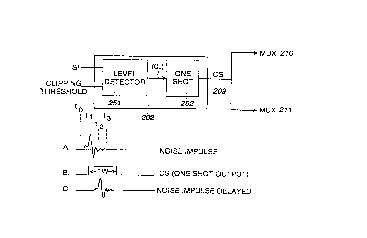
Fig. 2 shows a threshold detector 202 comprising a level ~letect~-r 2~1
driving a one shot 252. One shot 2~2 may be a mono,st~hle multivibrator or
any type of timing circuit or a~Tangement which produces, or provides, a
.
CA 02240679 1998-06-16
W O 97/24802 PCT~US96/20326
desired pulse width in response to a triggering input signal. The threshold
(letect~r 202 of Fig. 2 is ~ nerl to have one shot 252 provide a pulse having
a pulse width 'l'W each time a noise impulse is sensed by level llet~tor 251
and its output (OL) goes from the iirst value (threshold level ~ot exceeded) to
~ 5 the second value (threshold level exceeded). Typically (as shown in w~vefu
A of Fig. 2) a noise impulse has a ~iling edge ~post cursor) and .~sr.ll~
about a l~el~ce level for a period of time shown to extend from time tl to t3
in w~v~o~ ~ The use of a one-shot (e.g., 252) g~n~r~t~s a pulse having a
width TW to create a window ~nrnmr~.~.cin~ the full rising and ~ilin~ edge
of the noise impulse as shown in W~v ~U~ S B and (:~ of Eig 2. Thus, in
response to a noise impulse, the one-shot generates a pulse during which the
adaptive filters of the receiver system are inhibited from adapting. Note that
typically the noise impulse also has a ~ sur (i.e., a period during which
the impulse builds up, as shown for time t0 to tl in wav~u~ A
A reason for pl~ring a delay network, such as 135, in the signal path is
to delay the prop~ n of the noise impulse and to trigger a one-shot such
that most (if not all) of the noise impulse (i.e., the ~ and the
pOSL~-SUl' of the noise impulse) occurs within the one-shot period and then
has little or no effect on the adaptation of the adaptive filters.
2 o A delay line is generally an expensive component and it is diffirlllt to
produce a delay line having the requisite time delay. It is therefore desirable,where pos.~ihl~, to ~n~ p~te the o~ ce of a noise impulse and use a
noise impulse predictor in conjllnr1i~ n with a one-shot like timing circuit to
inhihjt the adaptive filters.
Fig. 3 shows a threshold detector 202 which inrllld~s a noise impulse
predictor 253 in 7~ 1i*l n to the level detector 251 and one shot 252 already
CA 02240679 1998-06-16
W O 97124802 PCT~US96120326
shown in Fig. 2. The circuit of Fig. 3 is useful where the noise iInpulse shown
in wnv~Ol~u A of Fig. 3 occurs periodically or may be predicted. Ill the
~hsf~nre of noise impulse predictor 253, the level detector produces a pulse
upo~ the o~;ull~l.ce of the impulse and triggers one shot 252 to produce a
control signal (CS) to MUX210 and MUX211 following each noise impulse as
shown in wnv~ru~ CS of Fig. 3. The cing portion of the noise impulse is
allowed through the circuit and may adversely affect the adaptive filters if
there is insuffiri~nt delay before the filters are inhihitell as tliccllcsed above.
Thus, where the noise impulse has a repetitive pattern, or its occulle~ce can
be predicted, use is made of noise impulse predictor 253 which filnrtinnc to
produce pulses, as shown in wnv~l... B of Fig. 3, in anticipation of each
noise pulse. The anticipatory pulses (B) are coupled through OR gate 254
and trigger one shot 252 c~ ing the signal CS to be mo~ifi~d as shown i~ he
CS MOD w~v~rulm in Fig. 3. The resultant pulses shown in the CS MOD
wnv~rullll become the .ci~n~lc applied tc the MUX210 and ~UX211.
Consequently, the control signal (CS) would inhihit the updating of the
adaptive filters of the ~ec~iver for a first period of 1;ime preceding the
oc~ ce of the noise impulse and a second period of time following the
o~ ce of the noise impulse. The setting of the co~.ffir.if~ntc of the adaptive
2 0 filters of the system are thus rendered relatively impervious to this type (i.e.,
repetitive or pre-lirtohle) of noise impulse. Noise impulse predictor 253 may
be part of a I ~oculltroller or state Tn~rhine (not shown) controlling va~ous
filnr,tionc; and operations of the l~v~r system.
In Fig. 1, each adaptive filter (e.g., FF filter 160) is adapted by feeding
25 an error signal (e.g., eQ) or a zero error co~.stsnt (e.g., EO) to a mlll1~pl~xer
(e.g., 210) and the output of the mul~lPxrr is then ~ed to a mlllh~ r (e.g.,
,
CA 02240679 1998-06-16
W O 97/24802 PCTnUS96/2032
111) whose output is then used to adapt the coPffiriPntc of the filter. This is
by way of illustration and it should be appreciated that there are other ways
and means to inhibit the adapting of the adaptive filters ~or .sPl~terl time
periods.
Fig. 4 shows certain details of an adaptive filter 400 which, for purpose
Of illllq~zlt;nn~ is :~.csllmefl to be the feed-rul ~Iv~d filter ~F). Huw~ver, filter
400 may be any other adaptive filter in the ~n.Cc~iver. The data input
finP~ the signal input to the filter. The data input .eign~l.s on input line 401are fed to a data delay line 403 which is controlled by a memory read line
signal 405 and a m~mory write line signal 407 generated by a l~iv~r
control~er circuit (not shown) The data .si~n~l.q d(n) produced by data delay
line 4û3 are output to a m~ ipliPr 409. The other input to mllltipli~r 409 is
the value of cof~-ffiri~n~-s (cn) provided at the output of coPffiri~nt storage 423.
The output of mllltirli~r 409 is supplied to adder 411 whose output is
supplied to ~ lm~ tor 413 whose output ~l~fines the filter output. One
mode of adjusting (~h:~n~in~) the coPffiM.on~s of the filter 400 innll~ s the
appli~ tinn of an error signal (eQ or EO) mlll1;plied by a of mlll~irlier 111 and
via line 136 to a coPffi~iPnt. updater 41~. Input .~ l.s to coPffini~nt. updater41~ in~ (lP the present coPffiniPnt value fc(n)] on line 417, the present data
value [d(n)] on liIle 419 and the value of the error ~signal (eQ or EO)
m ~ rlie~l by the value of a on line 136. CoPffi~ nt updater 415 may ~nrl~
a mlll~irlier 416 and an adder 418, as shown in Fig. 4~ Mnl1;~1iPr 416
mllltipliP~ the signal (eQ or EO) on line 136 with the data signal d(n) to
produce a ~ig~al denoted as DELTA. The DELTA signal is subtr~ftp-~l from
c(n) in adder 418 to produce c(n+l). Co~ iPnt updater 415 produces a new
,~ updated co~ffiriPnt value [c(n~1)] which may be expressed as follows:
CA 02240679 1998-06-16
W O 97/24802 PCTrUS96/20326
c(n+l) = c(n) - (a)(error .qignal)[d(n)] eq. 1
That is, a new (updated) value of the filter coPffi-~iPnt rc(n+l)] is equal to the
present value of the filter coPffi~iPnt {c(n)] minus a DELTA; where DELTA is
equal to the product of the mlllfiI liPr (a), the value of the error sig~al (eQ or
5 EO) and the value of the data input ld(n)].
In accordance with the showing of Fig. 1, the error signal eQ is set to
zero (i.e., "EO") when the input signal exceeds a threshold level. It should be
noted that inete~l of setting eQ to zero, the m~ll~li~r a may be set to zero
such that c(n+l) = c(n). Clearly, any means which causes c(n+l) to be equal
10 to c(n) in response to the (lptpc1;nn of a noise impulse Px~ee~ling a preset
threshold level is within the cnnf~ npl~tinn of the invention.
Tn~te~rl of contro~ing the value of c(n+l), it is possible to allow c(n+l)
to vary, but to inhihit its ~ula~;~ and future use, as ~liccllccell below. The
output [c(n+l)] of coPffi~.Pnt updater 415 is supplied to coPffi~Pnt storage 423which is cont~olled by a mPmOry read line 425 and a memory write line 427.
In Fig. 4, mPmory writ,e line 427 is shown e~mnecte~ to a logic gate 429 whose
output on line 431 is applied to coPffiriPnt storage 423 to control the writing of
the new va}ue c(n+l) into the coPffiriPnt storage. Acc~ .g to an aspect of
the invention, a control signal (CSA) is applied to logic gate 429 to prevent
20 the ~ a~;e of c(n+l) in coPffiriPnt storage 423 for the period of ~me that CSA
is in~lir~tive of a noise impulse exceeding a preset threshold (clipping) level. It should be evident that CSA is derived from ~ ~lrJ~ 202 and l~hat
controlling (inhihitin~) the storage of the updated value of the filter coPffi-~iPnt
is another way of inhihiting adaptation of the coPffiriPntq of the adaptive
25 filter when the noise impulse exceeds a dPqir~hle threshold level.
14
CA 02240679 1998-06-16
W O 97/24802 PCTrUS96/20326
In the circuit of Fig. 1, the threshold detection is pprfinrmed at the
output of the A/O cu~v~ller 134. Huw~ver, it should be noted lhat the noise
impulse (letec~ n can be p~rfor ne(l in the analog portion of the circuit at, orbefore, the input to the AID cullv~el.
The i,Iv~l,Lion has been ill~ ts~l for a single lac~iv~r rh~nn~.l but it
should be evident that the invention is apI lir.~hle to multi-rh~nnel lac~v~l-
systems.
It should be evident that the invention is applir~hle to inhibit
adaptation o~ any adjl~ct~hle circuit of the system, inr.llllling the phase-1Ocked
loop timing l~ov~L~ circuit (See block 133 in Fig. 1.). This may be better
.xpls~ined with l~fel~ce to Fig. 5 which shows more detail of the timing
Cuv~l~ loop.
Fig. 5 shows the output of A/D COllv~l ~ 134 conn~te~l to timing
l~uv~l~y band edge filters 501 which produce a timing vector applied to
phase-locked loop ~PLL) circuit 603. In accordance with the invention, PI.L
503 is controlled by means of a signal (cs) derived from (ietector 202. The
output 504 of the PIL is supplied to timing synt~.ci7.~r 505 to which is also
supplied a basic clock signal from o,srill~tor 507. Timingsyn ~ ~.ei7.~.r 505 then
produces the i~~iv~l~ s~mpling clock applied to A/D 134 tû s~mple the
2 o received .ei~nz~le and also generates a tr~n.~ s~mplin~ clock
applied to digital-to-analog co~v~llel 116. The PLL 503 (which in~ e
adaptive filt~rinE) provides a sig~al to sy~t)~.ei7.Pr 505 via line 504 which
filn~;~n.e to cause the syn~e~ei~pr to either increase the frequency ûf the
S~mI~ling clock, decrease the frequency of the s?.m~ling clock or cause the
2 5 frequency to remain the same. A noise impulse in the analog lect:i~e sig~al
causes distortion in the ou~put of the band edge filters which, in turn, causes
CA 02240679 1998-06-16
WO 97/24802 PCT~US96/20326
the PIL ou1;put to shift whereby the r~~iv~l .s:~mI lin~ clock will not have thee~cact frequency desired and 1~e received si~n~ will not be s~mIlled at the
pre~sely co~ect time. A~ gly, the flPtertor 202 supplies a s~gnal to PLL
503 inhihitin~ the frequency at the output of the synthe.~i7e ~o:m rhz~n~ing
5 during the pre~sence of a noise impuLse.
16