Language selection

Search

Patent 2241125 Summary

Third-party information liability

Some of the information on this Web page has been provided by external sources. The Government of Canada is not responsible for the accuracy, reliability or currency of the information supplied by external sources. Users wishing to rely upon this information should consult directly with the source of the information. Content provided by external sources is not subject to official languages, privacy and accessibility requirements.

Claims and Abstract availability

Any discrepancies in the text and image of the Claims and Abstract are due to differing posting times. Text of the Claims and Abstract are posted:

  • At the time the application is open to public inspection;
  • At the time of issue of the patent (grant).
(12) Patent Application: (11) CA 2241125
(54) English Title: VACUUM ASSISTED DEBRIS REMOVAL SYSTEM
(54) French Title: SYSTEME D'ENLEVEMENT DE DEBRIS PAR ASPIRATION
Status: Deemed Abandoned and Beyond the Period of Reinstatement - Pending Response to Notice of Disregarded Communication
Bibliographic Data
(51) International Patent Classification (IPC):
  • G03F 07/20 (2006.01)
  • H01L 21/00 (2006.01)
(72) Inventors :
  • MCCULLOUGH, ANDREW W. (United States of America)
  • OLSON, SEAN (United States of America)
(73) Owners :
  • INC. SVG LITHOGRAPHY SYSTEMS
(71) Applicants :
  • INC. SVG LITHOGRAPHY SYSTEMS (United States of America)
(74) Agent: OSLER, HOSKIN & HARCOURT LLP
(74) Associate agent:
(45) Issued:
(22) Filed Date: 1998-06-19
(41) Open to Public Inspection: 1998-12-19
Availability of licence: N/A
Dedicated to the Public: N/A
(25) Language of filing: English

Patent Cooperation Treaty (PCT): No

(30) Application Priority Data:
Application No. Country/Territory Date
08/878,633 (United States of America) 1997-06-19

Abstracts

English Abstract


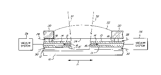
A vacuum manifold having a rectangular opening with vacuum
access bores connected into the rectangular opening for an
illumination field to be projected there through. A vacuum
manifold is placed between a photosensitive resist covered wafer
and a lens element in a photolithographic tool. The relatively
high illumination energy in an illumination field used for
projecting an image of a reticle onto a photosensitive resist
covered wafer often results in ablated, evaporated, and effused
material being coated on the lens element. The vacuum manifold
placed between the lens element and the photosensitive resist
covered wafer creates an airflow for removing debris or
contamination preventing coating of the lens surface. This
prevents image quality from degradation over time, as well as
reduces downtime needed for cleaning or maintenance of the
photolithographic tool.


French Abstract

Un aspirateur muni d'une ouverture rectangulaire avec des trous d'accès à la partie dépressurisée reliés à l'ouverture rectangulaire pour qu'un champ d'éclairage être projeté au travers. Un aspirateur est placé entre une plaquette enrobée de réserve photosensible et la lentille d'un appareil de photolithographie. L'énergie relativement élevée utilisée dans un champ d'éclairage pour projeter l'image d'un réticule sur une plaquette enrobée de réserve photosensible a souvent pour effet de recouvrir la lentille de matériau d'ablation évaporé et effusé. L'aspirateur placé entre la lentille et la plaquette enrobée de réserve photosensible engendre une circulation d'air qui élimine les débris ou les polluants et prévient ainsi l'enrobage de la lentille. Ce dispositif évite que la qualité de l'image ne se détériore avec le temps, et il réduit le temps d'immobilisation nécessaire au nettoyage ou à l'entretien de l'appareil de photolithographie.

Claims

Note: Claims are shown in the official language in which they were submitted.


What is claimed is:
1. A vacuum assisted debris removal system for use in
photolithography comprising:
a manifold having an illumination field opening placed
between a lens element and a photosensitive resist covered
substrate, said manifold having bores open to the illumination
field opening, and
a vacuum source coupled to said manifold,
whereby a flow pattern is obtained preventing the lens
element from being coated with debris.
2. A vacuum assisted debris removal system as in claim 1,
wherein:
said illumination field opening is rectangular having a pair
of longitudinal sides and a pair of lateral sides.
3. A vacuum assisted debris removal system as in claim 1,
wherein:
the bores are open along the pair of longitudinal sides.
4. A vacuum assisted debris removal system as in claim 3,
wherein:

the bores are open along the pair of lateral sides.
5. A vacuum assisted debris removal system as in claim 1,
further comprising:
a passage connecting the bores open to the illumination
field together, said passage connected at one end to said vacuum
source.
6. A vacuum assisted debris removal system as in claim 1,
wherein:
the bores open to the illumination field opening are spaced
substantially equally apart.
7. A vacuum assisted debris removal system for use in
photolithography comprising:
a vacuum manifold having a top substantially planar surface
and a bottom substantially planar surface, said vacuum manifold
having a rectangular illumination field opening formed therein
and a plurality of bores extending there through, the plurality
of bores having an axis of rotation substantially perpendicular
to the top and bottom substantially planar surfaces, the
plurality of bores having one end open to the rectangular
illumination field and another end coupled to a vacuum port, said
11

vacuum manifold mounted so as to be fixed with respect to
projection optics adjacent a lens element,
whereby debris and contamination is carried away from the
lens element preventing the lens element from being coated.
8. A vacuum assisted debris removal system for use in
photolithography as in claim 7 wherein:
said vacuum manifold is positioned adjacent the lens element
and a wafer such that a bottom air flow is created along the
bottom planer surface adjacent the wafer.
9. A vacuum assisted debris removal system for use in
photolithography as in claim 7 wherein:
said vacuum manifold is positioned adjacent the lens element
and a wafer such that an upper air flow is created along the top
planer surface adjacent the lens element and a bottom air flow is
created along the bottom planer surface adjacent the wafer.
10. A vacuum assisted debris removal system for use in
photolithography as in claim 7 wherein:
the rectangular illumination field has a pair of
longitudinal edges and a pair of lateral edges, the plurality of
bores being open along the pair of longitudinal edges.
12

11. A vacuum assisted debris removal system for use in
photolithography as in claim 7 wherein:
said plurality of bores having one end open to the
rectangular illumination field are spaced substantially equally
apart.
12. A vacuum assisted debris removal system for use in
photolithography comprising:
an illumination source having an illumination field;
a reticle placed adjacent said illumination source;
projection optics positioned to project an image of said
reticle and having a lens element;
a wafer stage positioned to receive at least a portion of
the image of said reticle;
a vacuum manifold placed between the lens element and said
wafer stage and fixed relative to said projection optics, said
vacuum manifold having a plurality of bores and an illumination
field opening therein sized to accommodate the illumination
field, the illumination field opening having a periphery, the
plurality of bores opening on the periphery of the illumination
field opening; and
13

a vacuum system coupled to the plurality of bores of said
vacuum manifold,
whereby airflow is created between the lens element and said
vacuum manifold and a wafer and said vacuum manifold preventing
the lens element from becoming coated with debris which degrades
performance over time.
13. A vacuum assisted debris removal system for use in
photolithography as in claim 12 wherein:
the illumination field is rectangular having a pair of
longitudinal sides and a pair of lateral sides.
14. A vacuum assisted debris removal system for use in
photolithography as in claim 12 wherein:
the plurality of bores are open along the pair of
longitudinal sides.
15. A vacuum assisted debris removal system for use in
photolithography as in claim 12 wherein:
the plurality of bores are substantially equally spaced
apart along the periphery of said illumination field.
14

Description

Note: Descriptions are shown in the official language in which they were submitted.


CA 0224112~ 1998-06-19
VACUUM ASSISTED DEBRIS REMOVAL SYSTEM
FIELD OF THE lNV~iNllON
The present relates generally to photolithography as used in
the manufacture of semiconductor devices, and more particularly
to a debris removal system used for preventing possible
contamination of the lens or other element that is closest to the
photosensitive layer by any byproduct or emanation from said
surface due either to residence time or the action of the actinic
or alignment wavelengths on the surface, the byproduct causing
contamination of the last element.
RI~CK~,ROUND OF THE lNV l':N'l lON
In the manufacture of semiconductor devices, the image of a
reticle is projected onto a photosensitive resist covered wafer.
In order to obtain the high resolutions desired, it is necessary
to bring a lens element or other element, that is part of the
projection optics close to the surface of the photosensitive
resist covered wafer. This distance may be as small as three mm.
This, in combination with high energy illumination systems

CA 0224112~ 1998-06-19
SVG-4026
sometimes used to project the image of a reticle may result in
ablated, evaporated, or effused material from the photosensitive
resist covered wafer in the process of exposure and/or by
background effusion with time of the material being inadvertently
deposited on the lens element. This reduces system performance
and is undesirable. Often, the lens element is difficult access
and to clean, and results in undesirable downtime of the
photolithographic tool or system. Additionally, the lens element
may be damaged during cleaning. While vacuum debris removal or
forced air systems have been used in very high laser cutters and
ablating systems, they are not applicable in photolithographic
systems where image quality must not be affected by the air flows
involved. Accordingly, there is a need for a system to prevent
the undesirable coating of a lens element with debris or
contamination materials in a photolithographic system.
SUMMARY OF THE lNv~NllON
The present invention prevents coating of a lens element
adjacent a photosensitive resist covered wafer. A vacuum manifold
having an illumination field opening therein is placed between
the last optical element of the projection optics and the
photosensitive resist covered wafer. Bores within the vacuum
manifold open to the illumination field opening. An upper gap is

CA 0224112~ 1998-06-19
SVG-4026
formed between the lens element and a top surface of the vacuum
manifold. A bottom gap is formed between a bottom surface of the
vacuum manifold and the photosensitive resist covered wafer.
Clean gas or air is drawn in along the upper gap and down, away
from the lens element, to the bores within the vacuum manifold
around the perimeter of the illumination field opening. Clean gas
or air is also drawn in along the bottom gap and out through the
bores, preventing contamination from reaching the lens element.
Some embodiments may not have a gap between the lens element and
the manifold. The absence of the upper gap does not preclude the
use and application of the invention. The airflow will be
different but a common principle is claimed.
Accordingly, it is an object of the present invention to
prevent possible coating of a lens element.
It is an advantage of the present invention that it does not
effect image quality.
It is a feature of the present invention that a manifold
vacuum system is placed between the lens element and the wafer.
These and other objects, advantages, and features will
become readily apparent in view of the following detailed
description.

CA 0224ll2~ l998-06-l9
SVG-4026
BRIEF DESCRIPTION OF THE DRAWINGS
Fig. 1 is a schematic diagram, in partial cross section,
illustrating the present invention.
Fig. 2 iS a plan view illustrating the present invention.
Fig. 3 is a cross section of line 3-3 in Fig. 2.
Fig. 4 iS a schematic diagram of a photolithographic system
using the present invention.
DETAILED DESCRIPTION OF THE PREFERRED EMBODIMENTS
Fig. 1 schematically illustrates a portion of the present
invention. A wafer 10 has a photosensitive resist coating 12
thereon. Wafer 10 is moved or scanned in a direction indicated by
arrow 11. Wafer 10 is generally placed on a stage, which is not
shown. A substantially planar manifold 14 iS placed adjacent the
photosensitive resist coating 12. The manifold 14 has a plurality
of side bores 16 therein. The manifold 14 iS attached to a
portion of the projection optics, for example lens mount 20, by
manifold mounts 18. A lens element 22 iS attached or held by lens
mount 20. The lens element 22 has a lens surface 24. The manifold
14 has a top surface 13 adjacent lens surface 24, and a bottom
surface 15 adjacent resist coating 12 on wafer 10. An upper gap
is formed between the lens surface 24 and the top surface 13, and
a lower gap is formed between the bottom surface 15 and the

CA 0224ll2~ l998-06-l9
SVG-4026
resist coating 12. A vacuum system 26 iS coupled to or
communicates with the side bores 16. Accordingly, the manifold 14
is placed between the wafer 10 having the photosensitive resist
coating 12 thereon and the lens surface 24. The distance between
the lens surface 24 and the photosensitive resist coating 12 on
the wafer 10 may be as small as three mm. The photolithographic
tool is generally placed in an environment having purged class I
air. The image of the reticle is projected by the projection
optics, including lens element 22, onto the photosensitive resist
coating 12. Rays 32 represent the electromagnetic radiation
forming an image as projected through a rectangular illumination
opening in the manifold 14. The ends of the manifold 14 may be
tapered or cut back to conform to the numerical aperture or cone
of light or illumination from the projection optics, including
lens element 22. Vacuum system 26 iS coupled or connected to side
bores 16. Accordingly, air is caused to flow down bores 16 to the
vacuum system 26. Airflow, represented by arrows 28, iS caused to
flow through the upper gap along the lens surface 24 and downward
through bores 16 adjacent the rectangular illumination field
opening. Additionally, gas or air is caused to flow, represented
by arrows 30, adjacent the photosensitive resist coating 12
through the lower gap and through the side bores 16 adjacent or
open to the rectangular illumination field opening. This gas or

CA 0224ll2~ l998-06-l9
SVG-4026
airflow pattern pushes or directs potential contaminates from the
photosensitive resist coating 12 away from the surface 24 of lens
element 22, and picks up debris from the photosensitive resist
coating 12 and carries it away preventing potential contamination
of lens surface 24. The manifold 14 remains stationary with the
projection optics as the wafer 10 is moved or scanned in the
direction of arrow 11.
Fig. 2 iS a plan view more clearly illustrating the vacuum
manifold 14 illustrated in Fig. 1. A longitudinal passage 34 iS
coupled or connected to a plurality of side bores 16. This
plurality is illustrated in principle: many configurations of
hole or bore size and distribution may have equivalent
functionality. The side bores 16 are open to the rectangular
illumination field opening 40, which generally conforms to the
rectangular illumination field used in the scanning
photolithographic tool. The rectangular illumination field
opening may be, for example, thirty millimeters long by eight
millimeters wide. The longitudinal passages 34 are connected to
lateral passages 38. End bores 36 are connected or coupled to
lateral passages 38. The end bores 36 are opened to the
rectangular illumination field opening 40. The longitudinal
passages 38 and the lateral passages 34 are connected or coupled
to a vacuum port 42. A vacuum system 26 iS then connected to

CA 0224112~ 1998-06-19
SVG-4026
vacuum port 42. If desired, a second vacuum port, not shown, may
be placed at the other end of the vacuum manifold 14 for the
placement of a second vacuum system, not shown. Generally, it is
only necessary to have side bores 16 opening along the opposing
longitudinal sides of the illumination field opening 40 to
provide sufficient gas or air flow to remove debris in most
applications. End bores 36 in most applications will not be
needed. The gas or air flow created by the vacuum manifold 14
need only be sufficient to remove debris, without adversely
effecting image quality. Preferably, the side bores 16 and the
end bores 36 are substantially equally spaced apart.
Fig. 3 is a cross section taken along line 3-3 in Fig. 2.
Fig. 3 more clearly illustrates the side bores 16 being opened to
the rectangular illumination field opening 40 and the
longitudinal passages 34. The end bores 36 are illustrated as
being circular, but may be of any cross sectional shape,
including rectangular. The bores 16 and 36 may be rectangular
openings made from a laminated structure.
Fig. 4 is a schematic diagram illustrating the present
invention in a photolithographic tool. An illumination source 132
provides illumination to a reticle 44, which is mounted on a
reticle stage 46. The image of the reticle 44 is projected by
projection optics 122 onto a photosensitive resist covered wafer

CA 0224ll2~ l998-06-l9
SVG-4026
116. The wafer 116 iS placed on a wafer stage 48. Stage control
50 controls the synchronous movement of the reticle stage 46 and
the wafer stage 48 to move or scan the wafer 116 in a direction
indicated by arrow 111. Typically, the projection optics will
provide a reduction of four to one, resulting in the reticle
stage moving at a different rate than the wafer stage. A vacuum
manifold 114 iS placed between the projection optics 122 and the
wafer 116. The vacuum manifold 114 iS attached to the projection
optics 122, and is therefore fixed with respect to the projection
optics 122. Vacuum system 126 iS coupled to the vacuum manifold
114.
Accordingly, debris and contamination, for example created
by the photosensitive resist coating on the wafer, is kept away
from the surface of the lens element, preventing its coating or
contamination. This increases system performance and prevents
degradation of image quality over time. As a result throughput is
increased because of less downtime and maintenance of the
lithographic tool. The airflow created by the present invention
should be sufficient to remove debris, but not so large so as to
influence image quality.
While the present invention has been illustrated and
described with respect to its preferred embodiments, it should be
apparent to those skilled in the art that various modifications

CA 02241125 1998-06-19
SVG-4026
may be made without departing from the spirit and scope of the
present invention.

Representative Drawing
A single figure which represents the drawing illustrating the invention.
Administrative Status

2024-08-01:As part of the Next Generation Patents (NGP) transition, the Canadian Patents Database (CPD) now contains a more detailed Event History, which replicates the Event Log of our new back-office solution.

Please note that "Inactive:" events refers to events no longer in use in our new back-office solution.

For a clearer understanding of the status of the application/patent presented on this page, the site Disclaimer , as well as the definitions for Patent , Event History , Maintenance Fee  and Payment History  should be consulted.

Event History

Description Date
Application Not Reinstated by Deadline 2003-06-19
Time Limit for Reversal Expired 2003-06-19
Deemed Abandoned - Failure to Respond to Maintenance Fee Notice 2002-06-19
Application Published (Open to Public Inspection) 1998-12-19
Inactive: Correspondence - Formalities 1998-09-18
Inactive: IPC assigned 1998-09-17
Inactive: First IPC assigned 1998-09-17
Classification Modified 1998-09-17
Inactive: First IPC assigned 1998-09-17
Filing Requirements Determined Compliant 1998-09-01
Inactive: Filing certificate - No RFE (English) 1998-09-01
Application Received - Regular National 1998-08-28

Abandonment History

Abandonment Date Reason Reinstatement Date
2002-06-19

Maintenance Fee

The last payment was received on 2001-05-29

Note : If the full payment has not been received on or before the date indicated, a further fee may be required which may be one of the following

  • the reinstatement fee;
  • the late payment fee; or
  • additional fee to reverse deemed expiry.

Patent fees are adjusted on the 1st of January every year. The amounts above are the current amounts if received by December 31 of the current year.
Please refer to the CIPO Patent Fees web page to see all current fee amounts.

Fee History

Fee Type Anniversary Year Due Date Paid Date
Registration of a document 1998-06-19
Application fee - standard 1998-06-19
MF (application, 2nd anniv.) - standard 02 2000-06-19 2000-04-19
MF (application, 3rd anniv.) - standard 03 2001-06-19 2001-05-29
Owners on Record

Note: Records showing the ownership history in alphabetical order.

Current Owners on Record
INC. SVG LITHOGRAPHY SYSTEMS
Past Owners on Record
ANDREW W. MCCULLOUGH
SEAN OLSON
Past Owners that do not appear in the "Owners on Record" listing will appear in other documentation within the application.
Documents

To view selected files, please enter reCAPTCHA code :


To view images, click a link in the Document Description column. To download the documents, select one or more checkboxes in the first column and then click the "Download Selected in PDF format (Zip Archive)" or the "Download Selected as Single PDF" button.

List of published and non-published patent-specific documents on the CPD .

If you have any difficulty accessing content, you can call the Client Service Centre at 1-866-997-1936 or send them an e-mail at CIPO Client Service Centre.


Document
Description 
Date
(yyyy-mm-dd) 
Number of pages   Size of Image (KB) 
Representative drawing 1999-01-11 1 8
Description 1998-06-18 9 271
Abstract 1998-09-17 1 24
Claims 1998-06-18 5 125
Drawings 1998-06-18 3 41
Courtesy - Certificate of registration (related document(s)) 1998-08-31 1 140
Filing Certificate (English) 1998-08-31 1 174
Reminder of maintenance fee due 2000-02-22 1 113
Courtesy - Abandonment Letter (Maintenance Fee) 2002-07-16 1 183
Reminder - Request for Examination 2003-02-19 1 112
Correspondence 1998-08-31 1 22
Correspondence 1998-09-17 2 52
Fees 2000-04-18 1 45
Fees 2001-05-28 1 42