Note: Descriptions are shown in the official language in which they were submitted.
CA 02241676 1998-06-25
WO 97/25745 PCT/US96/20164
Platinum-Free Ferroelectric Memory Cell
' with Intermetallic Barrier Layer and
Method of Making Same
FIELD OF THE INVENTION
s o The invention generally relates to ferroelectric structures integrated
onto
substrates such as silicon. In particular, the invention relates to metallic
barrier layers
interposed between the substrate and the ferroelectric stack.
BACKGROUND OF THE INVENTION
i5 Integrated circuit memory cells have become increasingly important as
personal
computers and other computerized equipment have found acceptance in many and
varied
applications. Dynamic random-access memory (DRAM) is currently the most
popular
type of randomly accessible memory for personal computers, but it suffers from
its need
to be periodically refreshed and its loss of information in the case of a
power failure or
2o system crash. Static RAM relies on flip-flop circuitry and does not need to
be refreshed,
but it still loses its contents when power is removed. Furthermore, it
requires
considerably more power than DRAM. Non-volatile memories have been developed
for
certain critical applications in which memory loss is not acceptable. These
range from
preprogrammed read-only memory (ROM) to electrically alterable non-volatile
memory,
25 but these impose operational or cost penalties relative to DRAM and are
difficult to
integrate to the 64- and 256-megabyte levels currently promised by advanced
DRAM
technology.
What is needed is a memory technology that offers not only non-volatile
storage
but also substantially no power requirement during prolonged storage and a
structure as
3 o simple as the capacitive storage of DRAM so as to allow dense integration.
Ferroelectric
memories have long offered the possibility of satisfying these requirements.
In very
-1-
CA 02241676 1998-06-25
WO 97/25745 PCT/US96/20164
simple terms, as illustrated in FIG. 1, a basic ferroelectric memory cell 10
includes two
capacitive electrodes 12 and 14 sandwiching in its capacitive gap a bistable,
polarizable
ferroelectric material 16. A bistable, polarizable ferroelectric has the
characteristic that
it can assume two stable polarization states, generally referred to as up and
down,
dependent upon a poling voltage applied to it. Once induced into one of these
polarization states, the polarizable material remains in the selected
polarization state for
very long periods of time. The polarization state determines the capacitance
experienced
by the electrodes 12 and 14. Hence, once a memory cell has been poled into one
of two
states, the state is thereafter held without further powering and it can be
read by
s o measuring the capacitance of the cell 10, that is, the ratio of charge to
voltage across the
cell. Furthermore, ferroelectrics typically manifest very high dielectric
constants in
either of their two states so that signal levels are relatively high compared
to the area of
the capacitors.
Although conceptually simple, a ferroelectric memory cell has been difficult
to
implement in an integrated circuit similar to a silicon DRAM. Materials
manifesting a
the largest ferroelectric behavior are metal oxides, typically having a
perovskite crystal
structure. Hence, their integration into silicon circuitry has proved to be a
major
problem. Integration with silicon is desirable not only because silicon
technology offers
the experience of a major industry over several decades, but also silicon
support circuitry
2 o is generally required to read, write, and otherwise control a dense
ferroelectric memory
array. Therefore, a commercially successful ferroelectric technology must be
integrated
with silicon materials and silicon processing. A greatly desired architecture
includes a
thin planar layer of a ferroelectric sandwiched between two electrode layers
in an
integrated vertical structure built upon a silicon substrate, similar to a
DRAM.
However, ferroelectrics integrated on a silicon substrate present some
fundamental problems. FerroeIectric materials are typically perovskites, such
as the
prototypical ferroelectrics PZT (lead zirconium zirconate) and PLZT (lead
lanthanum
zirconate) although many other perovskite ferroelectrics are known, such as
SrBiTaO
and other materials to be listed later. These perovskites are rich in oxygen
and usually
3 o need to be deposited at a relatively high temperature in a strongly
oxidizing
environment. As a result, the oxygen tends to diffuse out to the underlying
material, in
-2-
CA 02241676 2001-05-29
this case silicon. However, the semiconductivity of silicon is adversely
affected by the
incorporation of oxygen because of the ready formation of the insulating
silicon dioxide.
This integration of ferroelectrics with silicon has produced several designs,
each
with its own difficulties. A popular design has included platinum electrodes
sandwiching
the ferroelectric. The platinum, being a noble, refractory metal, resists the
diffusion of
oxygen from the ferroelectric down to the underlying silicon. However,
platinum is a
metal, and unless it is carefully grown it forms as a polycrystalline layer.
Hence, the
ferroelectric deposited over it also has a random orientation with a large
number of grain
boundaries, which cause problems with reproducibility and reliability. Another
approach
uses conductive metal oxides as the electrode material. Many of these
materials, such as
lanthanum strontium cobalt oxide (LSCO), have a perovskite crystal structure
similar to
that of the most common ferroelectrics, such as PLZT. As such, the perovskite
metal oxide
acts not only as the electrode but also as a growth template for the
perovskite ferroelectric.
The lower metal-oxide electrode can be deposited on a platinum layer without
the platinum
adversely affecting the ferroelectric layer. However, platinum still
introduces significant
difficulties in fabricating integrated circuits. Because platinum is highly
refractory, it is
very difficult to etch, and etching of almost every layer is required for
complex integrated-
circuit processing. At the present time, there is no known way of dry etching
platinum, that
is, using reactive ion etching. Ion milling platinum is known, but this
process introduces
debris onto the wafer being processed. Hence, it would be preferable if
platinum were
completely avoided, at least at the lower levels, in a ferroelectric memory
cell.
U.S. Patent 5,798,903 entitled "Electrode Structure for Ferroelectric
Capacitor
Integrated on Silicon" discloses that the platinum is not necessary and the
lower metal-
oxide electrode can be deposited directly on a TiN barrier layer, thus
eliminating the need
to etch platinum. However, this process is not proven, and the oxidation
temperature of
TiN and around 400°C instills doubts about depositing a metal oxide
above it.
It is thus desirable to eliminate platinum from the lower electrode in the
ferroelectric cell and find another material that is effective as a barrier to
the passage of
oxygen.
-3-
CA 02241676 2001-05-29
SUMMARY OF THE INVENTION
The invention can be summarized as an electrical element, such as a capacitor,
and
its method of making. The element is sequentially deposited on a substrate,
such as silicon,
and includes two electrodes sandwiching a layer of a ferroelectric or other
perovskite
material. Preferably, the electrodes are composed of a conductive metal oxide.
A barrier
layer of an intermetallic alloy is interposed between the bottom electrode and
the substrate
to prevent, among other problems, the oxygen from the oxygen-rich
ferroelectric or
electrodes from migrating downwardly and adversely affecting the underlying
substrate.
In accordance with one aspect of the present invention there is provided a
ferroelectric element, comprising: a substrate comprising semiconductive
silicon; a barrier
layer comprising an intermetallic alloy formed over said substrate; a first
electrode layer
comprising a metal oxide formed over said barrier layer; a ferroelectric layer
formed over
said first electrode layer; and a second electrode layer formed over said
ferroelectric layer.
In accordance with another aspect of the present invention there is provided a
method of forming an electrical element on a substrate, comprising the steps
of: depositing
a layer of an intermetallic alloy upon a substrate, said intermetallic alloy
has a composition
consisting substantially of AB, AZB ,A3B, ABZ or AB3, wherein A is selected
from the
group consisting of Fe, Cr, Co, Ni, Mn, Mo, and Nb and B is selected from the
group
consisting of Al, Ti, Cr, Si, Ru, Re, and W; depositing over said
intermetallic alloy a first
electrode layer comprising a metal oxide; depositing over said first electrode
layer a layer
of a perovskite; and forming over said perovskite layer a second electrode.
In accordance with yet another aspect of the present invention there is
provided a
perovskite element, comprising: a substrate; a barrier layer comprising an
intermetallic
alloy formed over said substrate, said intermetallic alloy comprising metals A
and B in
atomic ratios chosen from the group of compounds having stiochiometric ratios
selected
from the group AB, A2B, A3B, AB2, and AB3 and not deviating from said
stiochiometric
ratios by more than S atomic percent; a first layer comprising a conductive
metal oxide
formed over said barrier layer; and a perovskite layer comprising a perovskite
material
formed over said first layer.
In accordance with still yet another aspect of the present invention there is
provided
a perovskite element, comprising: a substrate; a barrier layer comprising an
intermetallic
-4-
CA 02241676 2001-05-29
alloy formed over said substrate, wherein said intermetallic alloy consists
essentially of
one of AB, A2B, A3B, AB2 and AB3 wherein A is selected from the group
consisting of Fe,
Cr, Co, Ni, Mn, Mo, and Nb and B is selected from the group consisting of Al,
Ti, Cr, Si,
Ru, Re and wherein said intermetallic alloy does not deviate from one of said
AB, AZB,
A3B, ABz and AB3 by more than 5 atomic percent; a first layer comprising a
conductive
metal oxide formed over said barrier layer; and a perovskite layer comprising
a perovskite
material formed over said first layer.
BRIEF DESCRIPTION OF THE DRAWINGS
FIG. 1 is a schematical representation of a generic ferroelectric memory cell.
FIG. 2 is a cross-sectional view of a ferroelectric memory cell of the
invention
utilizing an intermetallic barrier layer.
FIG. 3 is an X-ray diffraction pattern for a vertical structure built
according to the
invention.
FIG. 4 is a cross-sectional view of a test structure incorporating a large
number of
ferroelectric capacitors of the invention.
FIG. 5 is a graph of hysteresis loops at two different temperatures for a
ferroelectric
capacitor built according to the invention.
FIG. 6 is a graph of hysteresis loops before and after imprinting for a
ferroelectric
capacitor of the invention.
FIGS. 7, 7A, and 7B are graphs at different fatiguing temperatures and cycling
rates
for various polarization components as a function of time while a
ferroelectric capacitor of
the invention is being fatigued.
FIGS. 8 and 8A are graphs showing the retention of logic states at two
different
holding temperatures.
-4a-
CA 02241676 1998-06-25
WO 97/25745 PCTlUS96/20164
FIG. 9 is a graph of the retention of the logic states for ferroelectric
capacitors
fabricated at different temperatures.
FIG. 10 is a graph of hysteresis loops for several devices with their
ferroelectrie
stacks deposited at different temperatures.
DETAILED DESCRIPTION OF THE PREFERRED EMBODIMENTS
We have discovered that a ferroelectric memory cell formed on a silicon
substrate by sequential depositions of layers can use a barrier layer of an
intermetallic
alloy that underlies the ferroelectric stack including its metal-oxide
electrodes and that
so preferably contacts the lower electrode. The resulting ferroelectric cell
has been found
to demonstrate superior electrical properties. Platinum does not need to be
included in
the structure of the memory. cell. An intermetallic alloy, as will be
explained more fully
later, has a composition of at least two metallic elements in a ratio that is
stoichiometric
or nearly so. Nickel aluminum (Ni3Al) is a prototypical intermetallic alloy.
Intermetallic alloys are well known for their resistance to oxidation at high
temperatures,
which is the environment faced by at least the bottom electrode during the
over growth
of a perovskite ferroelectric in an oxygen-rich environment at relatively high
temperatures. Thus, such a ferroelectric memory cell can be advantageously
used in an
integrated circuit incorporating large numbers of such memory cells.
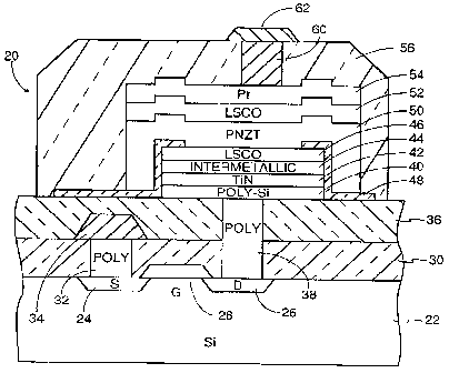
2 o An exemplary structure for a ferroelectric random access memory (FRAM) 20,
similar to a silicon dynamic RAM, is illustrated in cross section in FIG. 2.
It is
understood that this FRAM structure is replicated many times to form a large
FRAM
integrated circuit and that other support circuitry needs to formed as well in
the same
chip. The overall FRAM structure, with a few exceptions, is known and has been
disclosed by Ramesh in the previously cited U.S. patents and applications.
Kinney
provides a good overview in "Signal magnitudes in high density ferroelectric
memories,"
Integrated Ferroelectrics, vol. 4, 1994, pp. 131-144. The FRAM 20 is formed on
a
(001)-oriented crystalline silicon substrate 22 so that other silicon
circuitry can easily be
incorporated. A metal-oxide-semiconductor (MOS) transistor is formed by
diffusing or
s o implanting dopants of conductivity type opposite to that of the substrate
22 into source
and drain wells 24 and 26. The intervening gate region is overlaid with a gate
structure
-5-
CA 02241676 1998-06-25
WO 97/25745 PCT/US96/20i64
28 including a lower gate oxide and an upper metal gate line, e.g., aluminum
to control
the gate.
A first inter-level dielectric layer 30, fox example of silicon dioxide, is
deposited ,
over the substrate 22 and the transistor structure. A via 32 is
photolithographically
etched through the first inter-level dielectric layer 30 over the source well
24, and
polysilicon is filled therein to form a polysilicon contact plug to the
transistor source. A
metal source line 34 is photolithographically delineated on top of the first
inter-level
dielectric layer 30 and electrically contacts the polysilicon plug 32.
A second inter-level dielectric layer 36 is then deposited over the first
inter-level
so dielectric layer 30. Another via 38 is etched through both the first and
second inter-Ievel
dielectric layers 30, 36 over the area of drain well 26, and polysilicon is
filled therein to
form a contact to the transistor drain. The processing up to this point is
very standard in
silicon technology.
A lift-off mask is then deposited and defined to have an aperture over the
drain
s5 via 38 but of a larger area for the desired size of capacitor although in
commercial
manufacture a masked dry plasma etch would typically be performed in place of
the Lift
off. Over the mask and into the aperture are deposited a sequence of layers. A
polysilicon layer 40 provides good electrical contact to the polysilicon plug
38. A TiN
layer 42 forms a first conductive barrier layer between the polysilicon and
the oxidizing
2 o ferroelectric layer. Polysilicon is semiconductive, and, if its surface is
oxidized into
Si02, a stable, insulating layer is formed that prevents electrical contact.
Over the TiN Iayer 42 is deposited a layer 44 of an intermetallic alloy such
as
Ti3A1 to a thickness of about 100nm. Both the TiN layer 42 and the
interrnetallic layer
44 are conductive and act as barriers. Additionally, the titanium is a well
known glue
2s material, thus providing bonding between the underlying silicon and the
after deposited.
Titanium nitride was the originally used barrier material, but it suffers from
oxidation
above 450°C. As an alternative, the intermetallic layer can be used as
the only barrier
layer good at high and low temperatures, and it additionally provides bonding,
especially
when its composition is appropriately chosen, such as including titanium to
provide the
3 o glue function. That is, the invention includes a structure free of TiN or
similar barrier
layers of refractory nitrides.
_g_
CA 02241676 1998-06-25
WO 97/25745 PCTlUS96/20164
Over the intermetallic layer 44 is deposited a layer 46 of a conductive metal-
oxide, such as lanthanum strontium cobalt oxide (LSCO). This material has a
composition nominally given by La~.5Sr~5Co03, although compositions of
approximately
La~_XSrXCo03 are possible with 0.15?x?0.85. It is now well known that LSCO
forms an
acceptable electrical contact and further promotes highly oriented growth of
perovskites
ferroelectric materials. As mentioned before, because of the highly refractory
nature of
the intermetallic layer 42, the lower LSCO electrode 46 can be grown directly
on the
intermetallic layer 44, and this in turn can be grown directly on the silicon
40 without
the need of the TiN barrier layer 42.
1o It is understood that electrodes of materials other than LSCO may be used
with
the invention. Preferably they are formed of a conductive metal oxide, and
most
preferably a perovskite such as LSCO. See our previously cited patent
application for a
partial list.
The photomask is then lifted off leaving the lower stack of layers 40, 42, 44,
46
15 shown in FIG. 2. Another photomask is then defined allowing the conformal
deposition
of a Z-shaped field-oxide layer 48, which covers the sides of the previously
defined
lower stack, has a rim extending over the edge of the upper surface of the
lower stack,
and has a foot extending outwardly from the bottom of the lower stack, but
leaves a
central aperture for the after deposited upper ferroelectric stack. The field-
oxide layer
2 0 48 electrically insulates the after deposited ferroelectric from the side
portions of the
lower electrode. We explain in the above cited patent application, the field-
oxide layer
48 is preferably formed of bismuth titanate (Bi4Ti3Otz) or other highly
resistive
perovskites, although past practice has favored TiOz.
After the formation of the field oxide 48, another photomask is deposited and
2 5 defined that includes an aperture around the lower stack 40, 42, 44, 46
but the outer
periphery of its bottom overlies the feet of the field-oxide layer 48. A
ferroelectric layer
50 is then deposited under conditions favoring crystallographicalIy oriented
growth.
Preferably, the ferroelectric layer 50 comprises lead niobium zirconium
titanate (PNZT)
although the invention is not limited to this material. Many ferroelectric
materials are
3 o known, and a partial list of such materials will be presented later.
-7-
CA 02241676 1998-06-25 .,
WO 97/25745 PCT/US96/20164
Over the ferroelectric layer 50 is deposited an upper conductive layer 52.
Although not required by the invention, the upper conductive metal-oxide layer
52 is
preferably symmetrically formed with the Iower conductive metal-oxide layer 44
of a
perovskite, such as LSCO. The deposition of the perovskite ferroelectric layer
over
LSCO or other similar perovskite conductive electrodes allows the
ferroelectric to be
deposited at relatively low temperatures but still manifest favorable
crystallinity, and the
electrode symmetry reduces the asymmetry of ill-controlled electrical
characteristics.
An upper platinum layer 54 is deposited over the upper conductive metal-oxide
layer 52.
This layer 54 is not considered to involve critical technology, and its
platinum
1o composition was selected only as an interim solution. It is anticipated
that the
composition will be changed to TiW or other metallization common in silicon
technology. After the upper platinum layer 54 is deposited, the photomask is
lifted off
leaving the structure of the upper stack illustrated in FIG. 2.
A third inter-layer dielectric layer 56 is deposited and etched to cover the
z5 ferroelectric stack. This Iayer 56 is intended more as a passivation layer
than as an inter-
layer dielectric.
The upper electrode 54 is then electrically contacted by etching a via 60
through
the third inter-level dielectric layer 56 overlying the ferroelectric stack,
filling the via 60
with Ti/W, and delineating a metal capacitor line 62 of A1 that electrically
contacts the
2 o Ti/W plug 60.
This structure of the invention differs from that we disclosed in the
previously
cited patent application in that one conductive barrier layer is composed of
an
intermetallic alloy rather than of platinum. These alloys have been
intensively
investigated in the aircraft industry, particularly for jet turbine blades,
because of their
25 toughness, strength, and resistance to corrosion at high temperatures, in
the 800 to
1200°C range, in the highly corrosive and oxidizing jet-engine exhaust.
Much of this
work is referenced in the MRS proceedings: ( 1 ) High Temperature Ordered
Irzternzetallic Alloys IV, Proceedings of Materials Research Society, vol.
213,
eds. Johnson et al, 1990; (2) High Temperature Ordered Irztermetallic Alloys
V,
so Proceedings of Materials Research Society, vol. 288, eds. Baker et al,
1992; (3) High
_g_
CA 02241676 1998-06-25
WO 97/25745 PCT/US96/20164
Temperature Ordered Internzetallic Alloys VI, Proceedings of Materials
Research
Society, vol. 364, eds. Horton et aI, 1994; and {4) Superalloys,
supercomposites and
superceramics, Material Science and Technology Series, eds. Tien et al.
(Academic
Press, 1989).
Intermetallic alloys are metallic alloys that typically consists principally
of two
metallic elements although ternary and higher-order intermetallic alloys are
possible.
Usually, at least one of the metals of the intermetallic alloy is refractory.
Also, the
literature is replete with suggestions to further improve the oxidation
resistance of
intermetallic alloys by appropriate doping, for example, of Nb and V
substituents to the
so limit of about 5 atomic % although doping up to 8 and IO% have been
reported. In
contrast to a metallic solid solution which can alloy over a continuously
variable and
relatively broad alloying percentage of its constituents, intermetallic alloys
are
characterized by the stoichiometry or near stoichiometry of their
constituents, that is,
two metals A and B can form a series of intermetallic alloys of composition
AB, AB2,
AB3, A3B, etc. Deviations from stoichiometry are typically limited to ~5
atomic %,
especially for intermetallic alloys of atomic component ratios of 3:1 and
less.
These alloys are similar to inorganic compounds such as NaCI where the two
ions Na and Cl are required to be in a fixed atomic ratio of 1:1. Although the
principal
compositions are based on Ni-Al, Ni-Ti, Nb-Li, and Nb-Al, there are many
derivative
2 o compositions of these alloys since many metals form such line compounds.
Interesting
examples exist in the series FeAI, CoAi, NiAI, and MnAl, some of which have
been
reported by Sands in U.S. Patents 5,169,485 and 5,075,755 for use in
electronic
applications.
Some preferred compositions for the intermetallic alloy are NiTi, Ni3Ti, NiAI,
2s Ni~AI, Ni3Nb, Nb3Al, NiW, and Co3Al. More general preferred families are
represented
by the chemical formulae AB, AB2, AB3, and A3B, where A is chosen from the
group of
Fe, Cr, Co, Ni, Mn, Mo, and Nb and where B is chosen from the group of Al, Ti,
Cr, Si,
~ Ru, Re, and W. Popular quaternary systems are {Co,Ni)3{AI,Ti) and
(Co,Ni)z(AITi).
Related intermetallic alloys such as TiAl and NiCo can be characterized as AA'
or BB'
3 o alloys, that is, components from only the A or B group. Two well studied
intermetallic
_g_
CA 02241676 1998-06-25
WO 97/25745 PCT/US96/20164
alloys are NiNb"_",9,Cr°.°~Ah_~ZS and NiNbo.2"SAl".o255. These
last two alloys are related to
Ni3Al, but with optimized compositions. As noted before, dopants, especially
vanadium
and niobium, may be substituted into the alloy.
Wet chemical etching of intermetallic alloys is well known. It is believed
that
s chlorine-based dry plasma etching can be adapted to intermetallic alloys in
a process
very close to standard etching of silicon integrated circuits.
A number of sets of samples were fabricated and tested in a number of
different
ways. The deposition was performed using pulsed laser ablation from a pulsed
KrF
excimer laser producing a laser fluence of 3J-cm z on the target being
ablated. Laser
s o ablation is a convenient method for testing new materials, but it is
anticipated that
chemical vapor deposition or physical vapor deposition will be used in
commercial
fabrication lines.
The deposition of the intermetallic layer and the ferroeleetric stack
including the
ferroelectric and sandwiching metal-oxide electrodes were performed in a
chamber at a
15 single temperature with the targets being remotely switched between the
layers. The
temperature was measured on the substrate holder, which is believed to be
about 20° to
40°C higher than the actual substrate temperature in the S00° to
650°C temperatures
employed in the reported experiments. The deposition apparatus deposited the
layers on
a crystalline silicon substrate precoated with a polysilicon layer and a
covering TiN
20 layer. The thickness of these layers were respectively 100 to 500nm and 50
to 70nm.
The intermetallic alloy was ablated from a target having a composition of
Ti;AI
with small amounts of Nb doping to the level of about 5 atomic °~'o.
The chamber
pressure during the intermetallic deposition was in the range of 10-6 to 10~'
Torr and was
essentially oxygen-free. The intermetallic layer was formed by 3000 shots of
the laser
25 and is believed to have formed to a thickness of about IOOnm. The
intermetallic alloy
was deposited at the same temperature as that used for the ferroelectric stack
only as a
matter of convenience, and its deposition temperature can be independently
optimized in
the range of room temperature to about 6S0°C.
The ferroelectric stack was deposited by pulsed laser ablation in an
environment
30 of 100 mTorr of O2. The stack consisted of electrodes of La".SSro.sCo03
(LSCO), each
having a thickness of about 100nm. The ferroelectric layer was composed of
-10-
CA 02241676 1998-06-25
WO 97/25745 PCTIUS96/20164
PbNb~,"4Zro.2$Ti~_6803 (PNZT), as determined from the target composition,
having a
thickness of 300nm. However, these conditions and this process are presented
only as an
. example. Many other conditions for laser ablation and other processes are
possible to
achieve the invention, for example, chemical-vapor deposition, plasma
sputtering, and e-
s beam sputtering.
Experiment 1
In one experiment, a wafer was deposited at 650°C for both the
ferroelectric stack
and the intermetallic layer. An X-ray diffraction pattern, shown in the graph
of FIG. 3,
was measured on an unpatterned wafer. The peaks are labeled with the Bragg
1o diffraction peaks identified to the various materials. Both the PNZT and
LSCO layers
show strong [001 ] perovskite Bragg peaks, indicating a preferred [001 ]
perovskite
orientation throughout the ferroelectric stack. The polysilicon peak was not
observed
because the polysilicon layer was only about 100nm thick. Importantly, the
diffraction
pattern fails to show any pyrochlore-phase peaks, for example, one anticipated
at 35°.
15 That is, the entire ferroelectric stack seems to have grown in the
perovskite rather than
the pyrochlore phase.
Experiment 2
In a further elaboration of Experiment 1, the deposited layer was defined into
a
test structure, shown in the cross section of FIG. 4, incorporating a large
number of
2 o ferroelectric capacitors. The base structure consisted of a crystalline
silicon substrate 70
that was supplied with overgrown polysilicon and TiN layers 72, 74. The test
structure
included two alternative bottom contacting structures, one a direct bottom
contact and
the other a top capacitively-coupled top contact.
For the direct bottom contact, the principal capacitor area of the wafer was
2 s masked, an area for a bottom metal contact 75 was delineated, and the
platinum contact
material was deposited. This bottom-contact area was then masked, and the
ferroelectric-stack structure was deposited over the unmasked area. The
ferroelectric
stack structure was deposited by pulsed laser ablation to deposit an
intermetallic layer 76
of Ti3Al and a ferroelectric stack consisting of a lower LSCO electrode layer
78, a
3 o ferroelectric PNZT layer 80, and an upper LSCO electrode layer 82. The
particulars of
this deposition sequence and vertical structure are given above. The structure
was then
-11-
CA 02241676 1998-06-25
WO 97/25745 PCT/US96/20164
overlaid with a photolithographic lift-off mask for defining a platinum layer
86
principally into an array of capacitor dots 88 having diameters of SO~i,m, but
also
defining one or more large capacitor areas 90, which are much larger than the
relative
size illustrated in FIG. 4. The large capacitor areas 90 are used to provide
an effective
topside contact for the bottom electrode 78 by capacitively coupling to it.
Hysteresis measurements showed that the capacitive coupling configuration
produced slightly better ferroelectric effects, but the difference was small,
and the
following data will not differentiate the two configurations.
Pulsed laser ablation was used to deposit the platinum layer 86 over the
patterned
Z o lift-off mask, and the patterned Lift-off mask was then removed to leave
platinum pads
92, 94 defining the capacitor dots 88 and the large capacitor area 90. The so
defined
platinum pads 92, 94 were then used as shadow mask for a wet chemical etching
of the
upper LSCO electrode layer 78 by a 1 % HN03 aqueous solution, thereby
completing the
definition and electrical isolation of the capacitor dots 86 and the large
capacitive
s5 coupling area 88.
Each ferroelectric capacitor in the array can be electrically tested by probe
testing
both the platinum pad 92 associated with that capacitor dot 88 and either the
bottom
platinum contact 74 or one of the platinum pads 94 of the large capacitor
areas 90. The
capacitor dot 88 being probed defines the tested capacitive area. During
testing in a
2 o virtual ground mode, contact to the large capacitor area 90 acts only to
capacitively
couple into the conductive layers 70, 72, 74, 76, 78.
The resistivity of the PNZT layer 82 was measured to be 2x10 to l0y S2-cm2.
Hysteresis curves were measured for ferroelectric stacks grown at 650°C
at a room-
temperature (20°C) measurement, indicated by trace I00 in the graph of
FIG. 5, and at
25 a measurement temperature of 100°C, as indicated by trace 102. These
results indicate a
remanent polarization DP, that is, the difference between switched and
unswitched
polarizations, of 12.S~t,m/cm2 at SV and testing temperature of 20°C.
The imprint behavior was also measured with this sample, that is, the change
in
the hysteresis loops after the ferroelectric cell has been subjected to a
given bias over a
3 o fairly long period. In this experiment, the hysteresis loop was recorded,
and then the cell
CA 02241676 1998-06-25
WO 97/25745 PCTltTS96/20164
was biased at SV at 100°C for lhr to achieve the imprint. As shown in
the graph of
FIG. 6, the hysteresis loop 110 before imprinting does not significantly
differ from the
hysteresis Ioop 112 after imprinting at 100°C for lhr during which the
cell is impressed
with a single-sided pulse of 0 to SV at a frequency of 30kHz for a total of
10g cycles.
s Only a small coercive voltage shift occurred during the imprint stress.
The fatigue characteristics for this cell at room temperature are displayed in
the
graph of FIG. 7 for which the ferroelectric cell described above was stressed
with bipolar
square pulses of ~SV at 1 MHz with pulse polarization measurements being
performed
between the fatiguing pulses. This graph shows traces 120, 122 for unswitched
Zo polarization from respective positive and negative states and traces 124,
126 for the
respective switched polarization from corresponding states. These data show a
remanent
polarization DP of about I0.4E1.C/cm2 that does not significantly vary up to
10" cycles.
Corresponding fatigue characteristics at 100°C are shown in the graph
of FIG. 7A by
traces 120A, 122A, 124A, I26A. Other corresponding fatigue characteristics for
100°C
is and a cycle rate of 30kHz are shown in FIG. 7B by traces 120B, i22B, 124B,
126B.
These data indicate that the test conditions do not make a significant
difference. The
data at 30kHz cycling rate is particularly important since testing at IMHz can
be faulted
as never applying an effective voltage across the ferroelectric material.
The retention of logic states at room temperature is shown in the graph of
FIG. 8,
2o which shows the magnitude of various polarizations as a function of time
for a sample of
LSCO/PNZT/LSCO deposited at 650°C over TiN/polysilicon/crystalline
silicon with an
intervening intermetallic barrier layer of Ni3Ti. Traces 130, 132 show the
switched and
unswitched polarizations and traces 134, 136 show the switched and unswitched
remanent polarizations. Corresponding data for retention tested at
100°C are shown in
2 s FIG. 8A by traces 130A, 132A, 134A, 136A. These data show that higher
temperatures
do not deleteriously affect the ferroelectric characteristics. The retention
of logic states
for ferroelectric stacks grown at different temperatures is shown by the data
of the graph
of FIG. 9. The graph shows the difference of the switched and unswitched
polarizations
as a function of time. Trace 140 for a growth temperature of 550°C
shows a retention
-13-
CA 02241676 1998-06-25
WO 97/25745 PCTlLTS96/20164
life iRE.~. of 10 years; trace 142 at 600°C, a retention life of 10'
years; and trace 144 at
650°C, a retention Iife of 10" years.
The series of ferroelectric stacks grown at different substrate-holder
temperatures
were electrically poled. The resultant hysteresis loops are shown in FIG. 10.
Trace 150
s for the ferroelectric stack grown at 550°C showed a remanent
polarization OP of
8.6~C/cm2; trace 152 for the stack grown at 600°C showed a OP of
10.7~.C/cm''; and
trace 154 for the stack grown qt 650°C showed a dP of 12.51,tC/cmz.
Fatigue data for
these samples were measured and showed that the remanent polarization did not
significantly vary from ~10~.C/cm2 for samples fatigued up to 6x10"' cycles of
~5V at
so lMHz, regardless of whether the ferroelectric stack was deposited at 550,
600, or 650°C.
The above described embodiments are intended to be only exemplary and not at
all limiting. Many variations are anticipated, and others are included within
the
invention as defined by the claims.
The ferroelectric layer may be formed from several different families of
z5 ferroelectric materials, Pb,_YLaY(Zr, Ti, Nb)03, Bai_XSrxTi03,
PbNbZrTiO,and
BiSr(Ta,Nb)O being among the most presently popular choices. Lines and Glass
provide a fairly comprehensive list of ferroelectric materials, in Principles
and
Applications of Ferroelectrics and Related Materials, (Clarendon Press, 1977),
pp. 620-
625.
2 o The perovskite electrodes may be formed of other materials, such as
(Sr, Ca)Ru03, LaSrVO, YBaCuO, and BiSrCaCuO among others. Many of these have
been thoroughly investigated for low-T~ superconductivity. Our previously
cited patent
application also describes metal-oxide electrodes having the rock-salt crystal
structure,
such as NdO, NbO, SmO, LaO, and VO.
25 The TiN barrier layer can be replaced by a number of other materials that
are
electrically conductive compounds of a refractory metal and an anion,
especially
nitrogen. The most prominent of these are titanium tungsten nitride and
tantalum silicon
nitride.
Although the invention has been explained in the context of the integration of
a
3 o non-volatile ferroelectric capacitor on a silicon chip, presently the most
commercially
_14_
CA 02241676 1998-06-25
WO 97/25745 PCT/US96/20I64
important use being contemplated, the invention is not so limited. The
perovskite
material need not be a bistable ferroelectric. Other perovskites, especially
some
ferroelectrics, demonstrate very large dielectric constants but are not
bistable. That is,
such a ferroelectric capacitor has a very large capacitance per unit area but
does not
provide a volatile memory, only a large capacitance or a small volatile memory
cell.
Also, perovskites may be incorporated into superconducting circuit elements
and various
magnetic sensors and other devices.
Also, even though silicon substrates present particular advantages for
integration
with ferroelectric elements, the invention can be applied to integration with
other
so substrates, whether passive, such as glassy silicates, silica, or other
ceramics, or other
types of semiconductors, such as GaAs.
The invention thus provides ready electrical contacts to perovskite materials,
especially ferroelectrics, and assures the reliability and lifetime of the
resultant electrical
element. It additionally acts as a barrier preventing the migration of
deleterious
s s elements in either direction through the electrode. The intermetallic
barrier can replace
the previously used platinum barrier and is much more amenable to the etching
required
for integrated-circuit fabrication. Also, the oxidation-resistant
intermetallic barrier layer,
with or without the underlying TiN barrier layer, allows deposition of the
perovskite
layers at higher temperatures above 600°C in an oxidizing environment
without the
2 o underlying silicon from being oxidized.
Thereby, the intermetallic barrier layer provides beneficial device
characteristics
while being amenable to easy, large-scale commercial processing.
-15-