Note: Descriptions are shown in the official language in which they were submitted.
RD-26,230 CA 02241678 1998-06-25
-1-
SILICON DIOXIDE DEPOSITION BY PLASMA
ACTIVATED EVAPORATION PROCESS
This invention relates to deposition of thin stable, adherent
abrasion resistant films or coatings on various surfaces, particularly
plastic surfaces and to articles having such coatings.
BACKGROUND OF THE INVENTION
Engineering resins are well-known, commercially available
materials possessing physical and chemical properties which are
useful in a wide variety of applications. For example,
polycarbonates, because of their excellent breakage resistance,
have replaced glass in many products, such as automobile
headiamps and stoplight lenses; safety shields in windows,
architectural glazing, and the like. However, major defects exhibited
by polycarbonates are their very low scratch-resistance and their
susceptibility to ultraviolet light-induced degradation.
Several techniques for depositing silicon films are commonly
employed such as chemical vapor deposition (CVD), physical vapor
deposition(PVD), electron beam epitaxy and plasma enhanced
chemical vapor deposition (PECVD) and plasma polymerization
(PP). The choice of process is often dictated by the substrate to be
coated especially the thermal stability of the substrate which limits
the temperature to which it can be exposed. A primary goal is to
deposit hard, wear resistant, silicon films on plastic for a variety of
applications such as optical glass, architectural windows,
automobile windows, and the like. Key to production of such
products is the development of high rate low cost processes that
can deposit a high quality oxide film on the surface, particularly on
plastic surfaces. Physical vapor deposition techniques such as
RD-26,230 CA 02241678 1998-06-25
-2-
sputtering can yield good quality coatings but at low rates which are
not cost effective. High temperature chemical vapor deposition
techniques can yield high rates but at temperatures that exceed the
temperature limit of the substrate.
BRIEF DESCRIPTION OF THE DRAWINGS
Figure 1 is schematic illustration of an apparatus for coating
sheet material by the method of this invention.
Figure 2 is a schematic view of an apparatus for coating
flexible film.
SUMMARY OF THE INVENTION
Plasma activated reactive evaporation (ARE) is a process
which has been found to be suitable for deposition on low
temperature substrates such as plastics as well as on high
temperature materials such as ceramics and glass. This process
uses an electron-beam to evaporate silica or silicon at high rates in
the presence of nitrous oxide, an organosilicon, and an argon
plasma to nucleate and deposit dense films without exceeding the
temperature capability of the plastic. An additional oxygen inlet can
be used to provide oxygen in the case of non-oxide elemental
evaporation, and as make up oxygen when evaporating an oxide.
DESCRIPTION OF THE INVENTION
This invention provides a method for deposition of a hard,
stable, adherent, and abrasion resistant coating of silicon, carbon,
and oxygen on a substrate, e.g. a polycarbonate surface or a
polycarbonate surface which has been previously coated with a
silicone hard coat by any conventional means for depositing hard
coats such as dipping or rolling. A standard electron-beam is used
RD-26,230 CA 02241678 1998-06-25
-3-
to evaporate silica onto a plastic surface placed above the
evaporating silica in an evacuated chamber. Multiple hollow cathode
plasma sources are placed just below the substrate so that the
evaporating material and the substrate surface are exposed to the
plasma. A nitrous oxide gas flow is introduced just below the plasma
source so that the gas passes through the plasma to the surface
being coated. The presence of the nitrous oxide was unexpectedly
found to improve the stability of the coating and alter the stress in
the coating. An organosilicon is also introduced just below the
plasma source so that it passes through the plasma. The presence
of an organosilicon was found to improve the ductility (as measured
by % strain to micro-cracking) and the Taber abrasion resistance of
the coating.
Organosilicon modified oxide layers or thin films having
improved flexibility, which are resistant to cracking, delamination,
and abrasion can be deposited on substrate surfaces by a process
which combines features of physical and chemical vapor deposition
techniques in the presence of a plasma. A small amount of at least
one suitable organic monomer improves the properties of the film.
The reactive gas and the monomers together with the vaporized
oxide-forming element, such as an elemental metal like titanium,
aluminum, or silicon or a-metal oxide such as silicon dioxide are
supplied to the reaction chamber so that they pass through a high
density plasma before contacting the substrate surface on which the
film is to be deposited. Passing the reactive gas, the oxide
precursor, and the monomer through the plasma prior to
impingement on the surface improves the layer structure and its
properties.
Silicon-containing reactive monomers include silane, disilane,
or organosilicon compounds such as tetramethyldisiloxane
RD-26,230 CA 02241678 1998-06-25
-4-
(TMDSO), hexamethyldisiloxane (HMDSO), tetraethyl orthosilicate,
hexamethyldisilane, octamethylcyclotetrasiloxane (D4), and
tetramethylcyclotetrasiloxane.
DESCRIPTION OF THE DRAWINGS
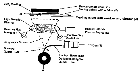
Fig. 1 shows a preferred embodiment of the invention in
which the substrate 1 is a plastic sheet which is placed on top of the
moving palette 2. The sheet is located over the window in the
palette so that as it translates over the window in the cooling cover
3. It is exposed to the plasma, gases, and evaporating material.
Silica is evaporated from a rotating drum 4 by striking the surface
with an electron beam gun 5 that translates along the length of the
drum as the drum rotates. The beam is magnetically deflected as
routinely practiced. Multiple hollow cathode plasma sources 6 are
located just below the translating sheet and are magnetically
focused (not shown) to spread the beam for uniform plasma density
along the width of the sheet. Reactant gases such as nitrous oxide,
an organosilicon and/or oxygen are feed into the chamber through 2
gas manifolds 7 and 8 located on either side of the window and
below the plasma so that the gases pass through the plasma and
react with the evaporating materials. Typically, the chamber is
pumped down to a set pressure to remove residual moisture from
the chamber. The pressure is then increased via the argon supply to
the hollow cathodes and the oxidant feed. After adjustment of the
silica evaporation rate and obtaining a stable plasma density, the
shutter covering the opening (window) in the cooling plate is
opened. The speed of the palette 2 containing the plastic sheet to
be coated is then set to achieve the desired thickness based on the
evaporation rate.
RD-26,230 CA 02241678 1998-06-25
-5=
Deposits were made on 18 cm x 36 cm x 3 mm polycarbonate
sheet with and without a silicon hardcoat. The nitrous oxide and
oxygen flow rates were adjusted from 0 to 4 Vmin with equal flows to
the two gas manifolds. Organosilicon flow rates were adjusted from
0-4 grams/minute. The hollow cathode plasma were adjusted from 0
to 200 amps. The pressure during deposition ranged from 0.1 to 0.7
Pa depending on the gas flow rates. Deposition time was adjusted
to achieve a target thickness range of 2 to 4 microns.
Fig. 2 shows another embodiment of the invention. The
substrate 1 is a plastic film which runs from pay-out reel 2 to take-up
reel 4 via cooling drum 3. Silica is evaporated from a series of
resistance heated boat evaporators 5 arranged at the bottom of the
cooling drum 3. A pair of magnetrons 7 in front of the substrate are
used to generate the high density plasma. Arranged below the
plasma zone are nozzles 8,9,10, and 11 for the introduction of
nitrous oxide and other reactive or plasma gases. Nozzles are
directed towards the surface to be coated.
Example
A 18cm x 36cm x 3mm polycarbonate sheet was coated with
silicon dioxide in the following manner. Nitrous oxide was fed at 2
I/min through each of the two feed lines for a total flow of,4 I/min.
The chamber was pumped down to 0.21 Pa prior to deposition then
raised to 0.7Pa during deposition. Silicon was evaporated using a e-
beam current of 0.32 A which gave a deposition rate of about 250
nm/sec. The sheet passed over the evaporation source on a moving
palette with a speed of about 1 cm/sec to achieve a deposit
thickness of 4 microns. The hollow cathode current was set at 200
A. The plasma color was very light compared to the standard deep
purple argon plasma. The coating was very clear and well adhered
RD-26,230 CA 02241678 1998-06-25
-6-
to the polycarbonate sheet substrate. Visual inspection after several
weeks showed no change in appearance, adhesion, flaking, or
obvious reaction with air.
Examples 6, 7 were run in an analogous fashion with
variations in flow rate and plasma current as noted in Table 1.
Good results were obtained with low plasma or no plasma showing
the main benefit of this process. An added benefit of this process is
that the stress of the coating could be adjusted from tensile to
compressive stressed by controlling the feed rate of the nitrous
oxide.
Comparative examples 2-5 were run in an analogous fashion
with variation in the type of gas feed and the plasma current as
shown in Table 1. As shown, by comparison without a oxidant gas
feed reactivity with the air caused flaking of the coating independent
of the level of plasma activation. Using oxygen at high plasma
activation and high flow rate did result in a non-reactive coating but
the operating window was not sufficient since any lowering of the
feed rate or plasma current resulted in flaking of the coating.
Table 1 Silicon Dioxide Coating By ARE
Example Plasma Gas-Flow Stress Description of results
(amps) (Vm)
1 2x200 NZ0 2x2 T clear, no flaking, well adhered
2 2x200 - C flaking within minutes
3 2x200 02 2x1 T clear, no flaking, poor adhesion
4 2x200 02 2x0.5 T flaking within minutes
5 02 2x1 - flaking within minutes
6 - N20 2X2 T clear, no flaking, well adhered
7 2x125 N20 2x1 C clear, no flaking, well adhered
T = tensile stress
C = compressive stress
Examples 2-4 in Table 2 were run in an analogous fashion
with variation in organosilicon flow rate and plasma showing a
RD-26,230 CA 02241678 1998-06-25
-7-
second benefit of this process. The principle benefit of this process
is that the incorporation of an organosilicon increases the ductility
and abrasion resistance of the coating by using a combined CVD
and PVD approach to depositing the coating.
As shown, by comparison without an organosilicon gas feed,
the Taber abrasion and % strain to cracking were low. Using an
organosilicon increased the % strain to cracking and the Taber
abrasion, however, above a certain level it caused a decrease in
Taber abrasion.
Table 2 Silicon Oxygen Carbon Coating By ARE
Example HMDSO N20 Flow % Haze % strain % C
(g/m) (Vm)
1 0 2x2 18 0.8 0
2 1 2x2 12 1.2 2
3 2 W 4 1.5 6
4 4 2x2 13 1.9 12