Language selection

Search

Patent 2241851 Summary

Third-party information liability

Some of the information on this Web page has been provided by external sources. The Government of Canada is not responsible for the accuracy, reliability or currency of the information supplied by external sources. Users wishing to rely upon this information should consult directly with the source of the information. Content provided by external sources is not subject to official languages, privacy and accessibility requirements.

Claims and Abstract availability

Any discrepancies in the text and image of the Claims and Abstract are due to differing posting times. Text of the Claims and Abstract are posted:

  • At the time the application is open to public inspection;
  • At the time of issue of the patent (grant).
(12) Patent Application: (11) CA 2241851
(54) English Title: METHOD FOR MANUFACTURING A HOUSING PART WITH A SCREENING EFFECT FOR RADIO COMMUNICATION EQUIPMENT
(54) French Title: PROCEDE DE PRODUCTION D'UNE PARTIE BOITIER A EFFET DE BLINDAGE POUR MATERIEL DE RADIOCOMMUNICATION
Status: Deemed Abandoned and Beyond the Period of Reinstatement - Pending Response to Notice of Disregarded Communication
Bibliographic Data
(51) International Patent Classification (IPC):
  • H05K 9/00 (2006.01)
  • B29C 45/14 (2006.01)
  • H04B 1/10 (2006.01)
  • H04B 1/38 (2015.01)
(72) Inventors :
  • JOCHHEIM, EDGAR (Germany)
(73) Owners :
  • SIEMENS AKTIENGESELLSCHAFT
(71) Applicants :
  • SIEMENS AKTIENGESELLSCHAFT (Germany)
(74) Agent: SMART & BIGGAR LP
(74) Associate agent:
(45) Issued:
(86) PCT Filing Date: 1997-10-30
(87) Open to Public Inspection: 1998-05-07
Availability of licence: N/A
Dedicated to the Public: N/A
(25) Language of filing: English

Patent Cooperation Treaty (PCT): Yes
(86) PCT Filing Number: PCT/DE1997/002530
(87) International Publication Number: WO 1998019507
(85) National Entry: 1998-06-26

(30) Application Priority Data:
Application No. Country/Territory Date
296 19 002.0 (Germany) 1996-10-31

Abstracts

English Abstract


The invention relates to a method for manufacturing a housing part with
screening functions and a housing part with screening functions for a
radiocommunication equipment having saucer-type housing parts with overlying,
facing open sides to lodge the radiocommunications device. To shorten the
manufacturing process by one step, a wire web which has been cut according to
the inner contours of the housing part is introduced in an injection mould for
the screening housing part. In said wire web, all contact surfaces and their
counterparts are coated with a foil corresponding to the dimensions of the
desired contact surface. The foils are removed after subsequent injection
moulding with insulating material.


French Abstract

L'invention concerne un procédé de production d'une partie boîtier dotée d'une fonction de blindage et une partie boîtier avec fonction de blindage pour un matériel de radiocommunication comprenant des parties boîtier en forme de coques assemblées par leurs côtés ouverts et destinées à loger le dispositif de radiocommunication. Pour supprimer une étape de production, on introduit dans un moule pour moulage par injection destiné à la partie boîtier à blinder un tissu métallique découpé d'après les contours intérieurs de la partie boîtier à effet de blindage. Toutes les plages de contact de ce tissu métallique sont, avec leurs contre-éléments de contact, revêtues d'un film ayant les dimensions des plages de contact souhaitées et, au terme du procédé de moulage par injection réalisé avec un matériau isolant, les films sont retirés.

Claims

Note: Claims are shown in the official language in which they were submitted.

- 5 -
Claims
1. Method for manufacturing a housing part having a
screening function for a radio communication device
having saucer-shaped housing parts lying on top of one
another with their open sides facing each other to
accommodate the radio communication device,
c h a r a c t e r i z e d t h e r e i n
that a wire web which has been cut according to the inner
contour of the housing part is introduced in an injection
mold for the screening housing part, all contact surfaces
and their counterparts in said wire web being coated with
a foil corresponding to the dimensions of the desired
contact surfaces and that, after the subsequent injection
molding with an insulating material, the foils are
removed.
2. A method according to claim 1,
c h a r a c t e r i z e d t h e r e i n
that adhesive foils are used for the coating.
3. A housing part which has been manufactured according to
the method of either claim 1 or 2,
c h a r a c t e r i z e d t h e r e i n
that the uncoated surfaces (11) of the wire web (10)
which are located on the inner sides of the housing part
(6) after the manufacturing process, which establish a
low-resistance contact at the connection to a
counterpart, e.g. a mass surface on the printed circuit
board (7) component.

Description

Note: Descriptions are shown in the official language in which they were submitted.


CA 022418~1 1998-06-26
Description
Method for manufacturing a housing part with a screening
effect for radio communication equipment.
The present invention concerns a method for manufacturing a
housing part with a screening effect and a housing part with
a screening function which has been produced according to this
method, for a radio communication device having saucer-shaped
housing parts lying on top of one another with their open
sides facing each other to accommodate the radio communication
device.
In radio communication equipment, e.g. mobile radio equipment
or wireless telephones, a screening is required to protect the
high-frequency and low-frequency logic components against
interfering radiation and interfering transmission of
electromagnetic rays. E.g. soldered screen frames, screen
baffles, metallized plastic housings, die-cast housings, etc.
may be used in a known manner for screening. Components of
this type increase the weight of the equipment, enlarge the
size of the equipment, increase the price of the equipment and
are very complicated to manufacture due to numerous difficult
assembly processes. The use of metallized or galvanized
plastic parts as housing parts is also complicated since two
completely separate steps with different machine tools are
required in each case.
The object of the invention is to manufacture, in a simple
manner, housing parts for a housing of the aforementioned type
which exhibit a good screening effect.
This object for a housing part of the aforementioned type is

CA 022418~1 1998-06-26
solved thereby that a wire web which has been cut according to
the inner contour of the housing part is introduced in an
injection mold for the screening housing part, all contact
surfaces and their counterparts in said wire web being coated
with a foil corresponding to the dimensions of the desired
contact surfaces and that, after the subsequent injection
molding with an insulating material, the foils are removed.
In the housing part manufactured according to the present
invention, the manufacturing problem of an additional
production step is solved since the housing part can be
manufactured in a single operation. Moreover, the invention
makes it possible to omit additional EMV seals which
previously had to be either inserted during assembly of the
housing or dispensed on by an additional process step.
A housing part in which a foil is sprayed on the back is known
from DE 19 515 010.4. However, the disadvantage of this known
housing part is that the foil cannot adapt to the existing
narrow radii and that, as a result, the foil can tear.
Further advantageous embodiments of the invention can be found
in the subclaims as well as in the following description of an
example of an embodiment shown in the drawings.
The invention shall be described with reference to an
embodiment illustrated in the drawings, showing:
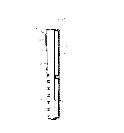
~IG. 1 a longitudinal section through a radio
communication device in which a housing part
manufactured by means of the method of the
invention is used,

CA 022418~1 1998-06-26
~IG. 2 a cross-section through the radio communication
device of FIG. 1 between the keys of the radio
communication device,
~IG. 3 a detail representation of the detail Y of a first
embodiment, and
~IG. 4 a detail representation of the detail Y of a second
embodiment.
The radio communication device 1 has a display 2 as well as a
keypad 3 on its upper side. An antenna 4 is affixed to the
upper face on the side. The housing of the radio
communication device consists of an upper shell 5 and a lower
shell 6 which lie on top of one another with their open sides
facing each other. The upper shell 5 has, inter alia,
openings for the display 2 as well as the keypad 3. A printed
circuit board 7 is arranged between the half shells 5 and 6
lying on top of one another to accommodate high-frequency
structural elements and logic components of the radio
communication device. To obtain an EMV screening, the lower
shell 6 must therefore be used as a screen. In the embodiment
shown, the lower shell 6 has two screened chambers 8 and 9.
According to the invention, the lower shell 6 is made by
spraying around and behind a wire web 10. For this purpose,
a wire web 10 which has been cut according to the inner
contour of the housing part 6 is introduced in an injection
mold for the screening housing part 6, in which all contact
surfaces and their counterparts are coated with a foil
corresponding to the dimensions of the desired contact
surfaces and, after a subsequent injection molding with
insulating material, the foils are removed.

CA 022418~1 1998-06-26
That is, the coated surfaces or the surfaces which are
uncoated after the injection molding process are sprayed on
the back, i.e. the wire web 10 is exposed on one side and the
uncoated surface of the wire web 10 is sprayed.
The exposed surfaces 11 form the electrical contact surfaces,
while the sprayed surface 12 as an inner insulation layer 12
acts in an insulating manner on possible structural elements
located on printed circuit boards to avoid a short circuit.
Due to the grid structure of the contact surfaces 11, i.e. of
the wire web 10, an additional seal can be omitted as a result
of the roughness given to the counterparts, e.g. in the type
of toothing.
Housing part 6, contact surfaces 11 and insulation layer 12
are produced in one production step.
FIGS. 3 and 4 show details in the contact area of the printed
circuit board on the shell edge in a detail representation.
In the embodiment according to FIG. 3, the wire web 10 is
thereby led to the upper side of the lower shell 6 to form a
contact with the mass surfaces of the printed circuit board 7
at this point. In the embodiment according to FIG. 4, the
inner side of the lower shell is stepped in the upper area,
whereby the printed circuit board 7 lies on the surface of the
step parallel to the printed circuit board 7 with its lower
side on the wire web 10, which produces a low-resistance
contact to the mass surfaces of the printed circuit board 7 at
the connection to the printed circuit board 7.

Representative Drawing
A single figure which represents the drawing illustrating the invention.
Administrative Status

2024-08-01:As part of the Next Generation Patents (NGP) transition, the Canadian Patents Database (CPD) now contains a more detailed Event History, which replicates the Event Log of our new back-office solution.

Please note that "Inactive:" events refers to events no longer in use in our new back-office solution.

For a clearer understanding of the status of the application/patent presented on this page, the site Disclaimer , as well as the definitions for Patent , Event History , Maintenance Fee  and Payment History  should be consulted.

Event History

Description Date
Inactive: IPC from PCS 2022-09-10
Inactive: IPC expired 2015-01-01
Inactive: IPC expired 2009-01-01
Inactive: IPC from MCD 2006-03-12
Inactive: Dead - RFE never made 2003-10-30
Application Not Reinstated by Deadline 2003-10-30
Deemed Abandoned - Failure to Respond to Maintenance Fee Notice 2003-10-30
Inactive: Abandon-RFE+Late fee unpaid-Correspondence sent 2002-10-30
Inactive: IPC assigned 1998-09-25
Classification Modified 1998-09-25
Inactive: IPC assigned 1998-09-25
Inactive: First IPC assigned 1998-09-25
Inactive: IPC assigned 1998-09-25
Inactive: Notice - National entry - No RFE 1998-09-10
Application Received - PCT 1998-09-08
Application Published (Open to Public Inspection) 1998-05-07

Abandonment History

Abandonment Date Reason Reinstatement Date
2003-10-30

Maintenance Fee

The last payment was received on 2002-09-20

Note : If the full payment has not been received on or before the date indicated, a further fee may be required which may be one of the following

  • the reinstatement fee;
  • the late payment fee; or
  • additional fee to reverse deemed expiry.

Please refer to the CIPO Patent Fees web page to see all current fee amounts.

Fee History

Fee Type Anniversary Year Due Date Paid Date
Basic national fee - standard 1998-06-26
Registration of a document 1998-06-26
MF (application, 2nd anniv.) - standard 02 1999-11-01 1999-09-15
MF (application, 3rd anniv.) - standard 03 2000-10-30 2000-09-19
MF (application, 4th anniv.) - standard 04 2001-10-30 2001-09-19
MF (application, 5th anniv.) - standard 05 2002-10-30 2002-09-20
Owners on Record

Note: Records showing the ownership history in alphabetical order.

Current Owners on Record
SIEMENS AKTIENGESELLSCHAFT
Past Owners on Record
EDGAR JOCHHEIM
Past Owners that do not appear in the "Owners on Record" listing will appear in other documentation within the application.
Documents

To view selected files, please enter reCAPTCHA code :


To view images, click a link in the Document Description column. To download the documents, select one or more checkboxes in the first column and then click the "Download Selected in PDF format (Zip Archive)" or the "Download Selected as Single PDF" button.

List of published and non-published patent-specific documents on the CPD .

If you have any difficulty accessing content, you can call the Client Service Centre at 1-866-997-1936 or send them an e-mail at CIPO Client Service Centre.


Document
Description 
Date
(yyyy-mm-dd) 
Number of pages   Size of Image (KB) 
Representative drawing 1998-09-29 1 4
Abstract 1998-06-26 1 24
Description 1998-06-26 4 158
Claims 1998-06-26 1 34
Drawings 1998-06-26 2 26
Cover Page 1998-09-29 1 49
Notice of National Entry 1998-09-10 1 209
Courtesy - Certificate of registration (related document(s)) 1998-09-10 1 140
Reminder of maintenance fee due 1999-07-02 1 112
Reminder - Request for Examination 2002-07-03 1 128
Courtesy - Abandonment Letter (Request for Examination) 2003-01-08 1 167
Courtesy - Abandonment Letter (Maintenance Fee) 2003-12-29 1 177
PCT 1998-06-26 8 286