Note: Descriptions are shown in the official language in which they were submitted.
CA 0224294~ 1998-07-06
SAR 12427 ' ~ ~ I EI418846018US
METHOD AND APPAE~ATUS FOR REMOTELY
IDEl~ YL~G AN ELECTRON~CALLY CODED ARTICLE
This application claims benefit of U.S. provisional patent application
serial number 60/052,135, filed July 10, 1997.
This invention relates to systems remotely identifying electronically
coded articles, e.g., tags or badges. More particularly, the invention provides
an ability to rapidly identify a coded article, even when multiple articles are
10 simultaneously present in an interrogation area.
BACKGROUND OF THE INVENTION
Commonly assigned U.S. patents 5,502,445, issued March 26, 1996 and
5,491,482, issued February 13, 1996 disclose a system and method for remotely
15 identifying electronically coded articles (e.g., tags, badges and the like). Each
of these patents is herein incorporated by reference. The system is comprised
of an interrogation and identification (I/I) unit (also referred to as simply aninterrogator) and a plurality of badges. The interrogator sends a microwave
signal to the badges within a defined area near the interrogator, i.e., the
20 interrogation area. Circuitry within each of the badges processes the
interrogation signal and, in response to the interrogation signal, the badges
transmit a signal back to the interrogator. From the responsive signal, the
interrogator identifies each of the badges by analyzing certain modulation
encoded onto the return signal.
26 More specifically, each of the badges contains a plurality of ID registers
(e.g., an A-register, a B-register, and so on) that store unique identification
values, i.e., although a particular value in a particular register is not unique,
the values in a plurality of registers taken together uniquely identify the
badge. The interrogator causes each badge to retrieve the identification values
30 and send the values to the interrogator. To accomplish badge identification,
CA 0224294F7 1998-07-06
S~R12427 EI418846018US
-2-
the system performs a "two pass" process. During the first pass, the system
generates an interrogation beam to activate the badges within the
interrogation area. The system repeatedly sends an interrogation signal that
causes the badges to transmit values from their ID registers. This pass causes
5 all the values from each register to be sent, i.e., request the data in all the A-
registers of all the badges within the interrogation area, then request data
from all the B-registers, then all the C-registers, and so on. The identification
values are stored in a computer coupled to the interrogator. The computer
then categorizes the values into groups defined by the specific register within
10 the badge from which the value was retrieved, i.e., each returned value is
stored in an array that correlates the various values with the various registers.
During a "second pass", the categorized groups are sorted by sending particular
coding combination to the badges where the coding combination is derived from
an analysis of the categorized values. The specific coding combinations
15 uniquely identify the badge that responds to the second interrogation signal.To accumulate the data from the ID registers, the present system
repeatedly polls the badges that are within in the interrogation area to retrieve
the register data one register at a time, i.e., all the A-registers are polled, then
all the B-registers, and so on. This one-value at a time process is relatively
20 slow.
Therefore, there is a need in the art for a system and method for rapidly
identifying a plurality of electronically coded badges.
SUMMARY OF THE INVENTION
The present invention overcomes the disadvantages heretofore
associated with the prior art by providing an improved transceiver badge that
substantially improves the speed of a remote identification system.
Specifically, the invention is a system, and a concomitant method of operation
for the system, comprising a electronically coded article (e.g., a badge, tag, and
~ CA 0224294~ 1998-07-06
SAR 12427 EI418846018US
-3-
the like), an interrogator, and a computer. The interrogator transmits
predefined commands using a microwave signal, i.e., the interrogator transmits
an interrogation signal. The badge interprets the commands and transmits a
responsive signal. The computer then processes the returned data to identify
5 the badge.
More specifically, the badge contains a demodulator, a signal processor
and a modulator, where the demodulator and modulator are coupled to a
common antenna for receiving interrogation ~ign~ from an interrogator. The
demodulator is capable of demodulating the interrogation signal and providing
10 an encoded instruction to the signal processor. The signal processor contains a
counter, an instruction decoder, a comparator and a plurality of ID registers
cont~qining codewords that uniquely identify the badge. Although many
instructions are decoded by the instruction decoder, the instruction of interestis the instruction that "sets up" the signal processor components for responding16 to the interrogation signal. When the unique set up instruction is received, the
instruction decoder resets the counter to zero, selects a particular ID register,
and enables the comparator to compare the counter's count value to the
selected ID register content. After the set up instruction is sent by the
interrogator, the interrogator transmits a carrier wave (CW) signal that is
20 demodulated by the demodulator and produced as a square wave signal having
the same frequency as the CW signal. The square wave signal is divided by N
and used to clock the counter. Thus the counter increments on every Nth
count. Similarly, the interrogator, which is providing the CW signal, contains
a simil~r circuit that increments on every Nth count of transmitted CW cycles.
25 As such, the badge counter and interrogator counter are synchronized.
At each count of the counter, the badge's counter value is compared to
the selected ID register value (codeword). When a match occurs, the
comparator enables the modulator for the duration of the clock period and the
modulator sends a pulse to the interrogator. When the interrogator detects
~ CA 0224294~ 1998-07-06
SAR 12427 EI4188460 18US
-4 -
this modulation signal, it stores its internal count value (which is the same asthe current badge count value) in memory. This process is repeated for each ID
register until they have all been polled.
The computer then correlates the received ID register values of all the
5 badges that responded to the interrogation signal with the specific registers
that were polled. From that information, the interrogator can perform a
second scan of the badges to uniquely identify each badge. The second scan
process is disclosed in detail in U.S. patent 5, 502,445.
BRIEF DESCRIPTION OF THE DRA~iVINGS
The teachings of the present invention can be readily understood by
considering the following detailed description in conjunction with the
accompanying drawings, in which:
Fig. 1 is an illustrative schematic diagram of a remote identification
15 system that utilizes the transceiver badge of the present invention;
Fig. 2 is a block diagram of the transceiver badge of the present
invention;
Fig. 3 is a flow diagram of a process of identifying a remotely coded
article in accordance with an embodiment of the invention;
Fig. 4 is a waveform and timing diagram for the transceiver badge; and
Fig. 5 is a block diagram of an interrogator of the present invention.
To facilitate understanding, identical reference numerals have been
used, where possible, to designate identical elements that are common to the
figures.
DETAILED DESCRIPTION
FIG. 1 depicts a schematic illustration of an electronic interrogation and
identification (I/I) system 100 that comprises one or more interrogator/reader
(I/R) units 102, one or more badges (tags) 104, respective transmit and receive
' CA 0224294~ 1998-07-06
SAR 12427 EI418846018US
-5-
antennas 108 and 109, and a central computer 122. The I/R units operate at a
suitable radio frequency or microwave frequency (e.g., 13.56MHz) and transmit
microwave (radio frequency) beams 106. The badges 104 (which uniquely
identify individual employees) are interrogated by the beams 106 transmitted
5 from the directional antenna 108 of the I/R units 102 positioned at selected
locations. Each I/R unit 102, in addition, has a receiving antenna 109 which is
closely ~imil~r to the transmitting antenna 108. The I/R units 102 are
connected via respective cables 120 to a computer 122. In the course of being
interrogated via a microwave beam 106 from an I/R unit 102, a badge or
10 badges 104 reply electronically by transmitting a modulated signal back to the
receiving antenna 109 of the I/R unit 102. The modulated signal contains
various identification values that are stored in each badge. The badges 104
thus uniquely identify themselves in accordance with their respectively coded,
electronically stored ID numbers. As will be explained below, each badge may
15 be coded with any one of over 2NYB different numbers, where N is the number of
ID data registers and B is the number of bits per register. As soon as a badge
has been identified, its electronic circuit is placed in an inactive or "power
down" mode such that the badge does not continue to respond to the I/R
unit 102 for so long as that badge (once it has been identified) remains within
20 the range of the beam 106.
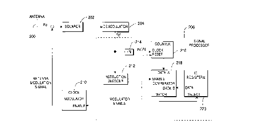
FIG. 2 depicts a block diagram of the transceiver badge 104 of the
present invention. The transceiver badge 104 contains an antenna 200, a
squarer 202, a demodulator 204, a signal processor 206 and a modulator 210.
The antenna 200 receives an interrogation signal transmitted by the I/R unit.
25 The antenna 200 is coupled to squarer 202 within which the interrogation
signal is converted into a logic level signal. The logic level signal is coupled to
the demodulator 204 which extracts binary encoded commands or data from
the received signals. The demodulator is coupled to the signal processor 206.
The signal processor 206 processes the demodulated signals to decipher any
CA 0224294~ 1998-07-06
SAR 12427 EI418846018US
-6-
particular instructions contained in the received interrogation signal. The
signal processor 206 also produces a responsive signal (e.g., modulator enable
signal) in response to the decoded information in the interrogation signal. The
responsive signal is coupled to the modulator 210. The modulator 210 is
5 coupled to the antenna 200 for transmitting a responsive signal to the I/R unit.
More specifically, the signal processor contains an instruction
decoder 212, a frequency divider 214, a counter 216, a comparator 218, and a
plurality of ID registers 220 cont~ining codewords that uniquely identify the
badge. The demodulator 204 is coupled to the instruction decoder 212. The
10 instruction decoder 212 sends control ~ign~l.s to other devices, such as the
counter 216, the comparator 218 and the registers 220, based on commands
received from demodulator 212. A comprehensive list of instructions that are
processed by the instruction decoder are provided in U.S. patent number
~,491,482.
The frequency divider 214 divides demodulated signals by N before they
are received by counter 216. The counter 216 is capable of counting each Nth
cycle and can be reset by the instruction decoder 212 to a count of zero. The
comparator 218 can compare the counter value (DATA-A) to the contents
(DATA-B) of any one of the data registers in ID registers 220 based on control
logic from instruction decoder 212. ID registers 220 are data storage registers
that contain the identification code, e.g., a 32-bit code can be stored in four 8-
bit codeword registers. In response to a modulator enable signal produced by
the comparator 218, modulator 210 applies a modulated signal to antenna 200
that is transmitted to the I/R unit.
In the following example, reference is made to ID registers A, B, C and
D, each of which is 8-bits wide. It should be understood, however, that the
invention can use any number of registers or register widths. Referring now
also to the flo-v diagram of FIG. 3 and the timing diagram of FIG. 4, the
operation of the invention begins at step 302 and proceeds to step 304 wherein
' CA 0224294~ 1998-07-06
SAR 12427 EI418846018US
-7-
a set-up instruction is sent from the interrogator 102 which, when decoded by
the instruction decoder 212, sets up the comparator 218 to compare the value of
the counter 216 to the contents of the A register in ID registers 220. This set
up instruction also resets counter 216 to zero. Immediately after transmitting
5 the instruction, an unmodulated rf signal (known as a carrier wave (CW)
signal) is transmitted by the interrogator (step 306). This CW signal is
converted by the demodulator 204 into a square wave version of input signal Fo
(i.e., signal Fo~ ). The divider 214 divides the square wave signal Fo~ by N and,
as such, the counter 216 begins to count each Nth cycle. Simultaneously, a
10 divider 501 and counter 502 in the interrogator 102 (see Fig. 5) also counts
each Nth cycle of the transmitted CW signal. Since the counter 216 is
counting based on the signal transmitted by the interrogator, counters 216 and
502 are synchronized. As such, the transceiver badge counter generates a
count value and the interrogator generates a count value "copy" that is
15 identical to the count value generated by the transceiver badge.
When, at step 308, the value in the counter 216 equals the value in
register A, the comparator 218 produces a signal (modulator enable) to the
modulator 210. The modulator 210 applies a signal to the antenna 200
(antenna modulation signal) for the duration of the Nth time interval (step
20 310). This signal applied to antenna 200 can be related to Fo~ such as by being
some multiple of Fo~ or a quotient in which Fo~ is a dividend. However, if two or
more tags have identical values in like registers, each will be transmitting this
identical signal at substantially identical times. Whereas the signal
transmitted by the two or more tags could be different in phase by 180~ with
25 respect to each other, cancellation of the .qjgn:~kq could occur. Preferably,therefore, the signal is generated by some other means known to those having
skill in the art, such as by including separate oscillators in each badge. In
another embodiment, individual tags could transmit at random times during
the duration of an Nth time interval. The antenna modulation signal applied
CA 0224294~ 1998-07-06
:. ' . ,,
SAR 12427 EI418846018US
-8-
to the antenna 200 is transmitted to and detected by detector 503 of
interrogator 102. When the interrogator 102 detects the modulated signal, its
counter indicates the value contained in the A register of ID registers 220. Forexample, the timing diagram depicts the modulator enable signal occurring on
5 a count of three, as such the A register contains the value of three.
At step 312, the interrogator continues transmitting a CW signal until N
x 256 cycles have been transmitted (256 = 2~ = the number of values that can
be represented in an eight-bit register). If there are multiple badges in the
field of operation, the interrogator may receive multiple responses during this
10 period. As noted above, if multiple badges have the same value in their A
register, they will activate their modulators simultaneously. The interrogator
need not distinguish between one or multiple badges simultaneously. At this
point the interrogator only needs to determine that some badge responded at a
particular time corresponding to a particular A-register value.
At step 314, the interrogator determines whether all the registers have
been interrogated. If not, steps 304 through 312 are repeated, except that the
instruction transmitted in step 304 is now changed such that the comparator in
the badge is set up to compare the counter output to the contents of the
B-register. Similarly, steps 304 through 312 are repeated for the C- and D-
20 registers, i e., until the condition at step 314 is true.
After this scan sequence has been performed for all the ID registers 220,
the interrogator contains a list of the possible register contents for each
register and for all badges located within the field of operation, i.e., the
interrogation area. However, if multiple badges are present, the interrogator
25 does not know which set of register values all belong to a particular badge. In
order to determine which set of values belong to each badge within the
operating field, a sorting routine is performed at step 316. This part of the
process is identical to the ~second pass" portion of the identification routine
described in the prior U.S. patent 5,502,445.
CA 0224294~ 1998-07-06
SAR 12427 EI4188460 18US
g
The time required to "scan" each register is the time required to transmit
a scan instruction, T" plus the time required for the badge to respond, Tr. For
8-bit wide registers, the response time Tr=256(N)(1/f), where f is the frequencyin Hertz of the CW signal. For the example discussed above, the entire pass of
5 the ID routine is therefore performed in approximately 4(TL+Tr) seconds. The
product (N)(1/f) is actually the bit period, P" for receiving data from the badge.
Assuming the commands have a length of 8-bits, the time to transmit the scan
command from the interrogator to the badge is approximately (8)(Pt), where Pt
is the bit period for tr~n~mi~.sion of data to the badge. For the four registers,
10 the entire scan time is therefore (1024)(Pr)+(32)(Pt). The actual time will be
somewhat longer due to sync bits and gaps between commands.
Depending on the transmit and receive bit rates of the system, this could
significantly reduce the time required to perform a first scan routine as
compared to the process disclosed in U.S. patent number 5,502,446. In that
15 method, for each possible register value, and for each register, a multi-bytecommand sequence is transmitted from the interrogator to the badge, and most
of these commands require time for a response from the bad~e. For the
example given here using four 8-bit registers, the interrogator would have to
send the following command sequence 255 times:
Data byte follows
Data byte (0-255)
Any Yes:
Match A?
Match B?
Match C?
Match D?
For the case where one badge is present, having four different values in its
registers, the prior art method requires a minimum of 784 comm~n-l~ must be
transmitted to the badge. Of these, 272 commands (those with a "?") must wait
CA 0224294~ 1998-07-06
SAR 12427 EI418846018US
-10-
for a response from the badge. Assuming 8-bit commands, a transmission bit
period of PL~ and a single bit response time of Pr~ the time required is
6272(P,)+272(Pr). For comparable bit rates, this prior art approach requires
considerably more time than the technique described above, i.e., the prior art
5 scan time of 6272 (P,)+272(Pr) compared to the scan time of the invention of
32(P~)+( 1024)(Pr)
Although various embodiments which incorporate the te~ching~ of the
present invention have been shown and described in detail herein, those skilled
in the art can readily devise many other varied embodiments that still
10 incorporate these teachings.