Note: Descriptions are shown in the official language in which they were submitted.
160 . 9 81 6 5 4u :\patents\word\2 51 7 2wo .doc CA 02243279 l 998 - 07 - l ~
OPTICAL MODUI I~TOR
This invention relates to an optical modulator, and more particularly to a discrete
modulator which modulates optical signals by electroabsorption. Electroabsorption
modulators (EAM) provide a convenient way of modulating optical signals, e.g. at wave
lengths of 1300nm and 1500nm, in a wide range of fibre optical systems. Using
sinusoidal voltage control for modulation they can generate short, e.g. having a duration
of less than 10ps, pulses. EAM are not only used to apply information carrying signals to
unmodulated optical signals but they are also used for the rapid switching of optical
signals, e.g. for demultiplexing of optical time division multiplexed signals.
It is important to distinguish between two forms of EAM, namely discrete and
laser integrated EAM. A laser integrated EAM is a single device, grown as a single entity
on the same chip, which includes a signal source (laser) and an EAM. The two functions
are arranged so that the EAM modulates the signal produced by the source. In a discrete
EAM the modulator is separate from the signal source, e.g. the signal is provided by fibre.
It will be apparent that integrated EAM cannot be used for applications where the signal
source must be separate, e.g. for demultiplexing or other applications where the signal
comes from a remote source. Tanaka et al in the Journal of Lightwave Technology,volume 4,number 9 of September 1990 pages 1357 - 1362 describe integral EAM which
include a thick layer of Fe-doped InP to provide electrical separation between the two
functions of single chip. Koren et al in Appl. Phys Letters Vol 51, No. 15 dated 12
October 1987 pages 1123 and 1124 describe discrete EAM with a large (4,um high and 6
,um wide) absorber region which is therefore multimode with a low modulation depth with
a slow switching speed. European patent specification 437836 relates to EAM and it is
particularly concerned with producing the capacitance between the electrodes. EPO
437836 is not at all concerned with modulation depth and it does not discuss how this
important property can be include.
It is emphasised that a discrete EAM is not integrated with the primary signal
source but it may be associated or integrated with other devices.
EAM are semiconductor devices and they are usually implemented in III/V
materials, for example materials containing at least one of indium, gallium or aluminium
together with at least one of phosphorus and arsenic. Some EAM are buried
heterostructure devices having a mesa or a ridge, usually formed of n-type material (such
as n-doped indium phosphide), which extends into an electrical
Ah1ENDED SHEET
CA 02243279 1998-07-1~
W O 97/36204 PCTIGB97/00505
blocking region such as iron doped indium phosphide. There is an absorber regionlocated on top of the mesa and this region provides a path for the optical signals to
be modulated., In order to provide the guidance the absorber region has a higherrefractive index than the material surrounding it. It will be appreciated that awaveguide comprises a path of higher refractive index surrounded by a cladding of
lower refractive index. Thus the absorber region and its surroundings constitute a
waveguiding structure. To achieve high modulation depths it is appropriate that
the absorber region support only a single optical mode. If there is more than one
mode, i.e. if there parasitic modes, then these will be transmitted in the
surrounding material. In other words, if there are more than one modes only one
tthe principle mode) mode is transmitted in the absorber region.
The absorber region is located between the top of the mesa and a cap
region, e.g. a cap region formed of p-doped indium phosphide. As is usual, a
semiconductor device comprises a p-doped region and an n-doped region. The
absorber region is located between these two regions. For example, the absorber
region is often located in the depletion region of a pin-junction which is reverse
biased. The absorber region may take the form of a single layer of semiconductormaterial with a uniform chemical composition having a suitable band gap.
Preferably, it takes the form of a multi quantum well (MQW) system which
consists of many, e.g. 19 to 49, interleaved layers of different semiconductor
materials. For exampie the MQW may consist of n layers (usually called "wells"I
of a first material and (n-1 ) layers (usually called "quantum barrier layers") of a
second material wherein n is 10 to 25. [There are a total of (2n-1 ) layers.] The
"wells" have a narrower band gap than the ~'barriers".
Quaternary semiconductors are particularly suitable for the absorber region
~single layer or MQW) because variations of the ratios of the (four) constituents
enables the band gap to be controlled as needed without adversely affecting the
other (crystallographic and electrical) properties. In III/V systems, the c~ùaternary
compounds contain indium, gallium, phosphorus and arsenic.
EAM work because the optical signals travei in the absorber region and the
absorption properties of this region are changed by the switching of an electricfield applied across the region. ~s mentioned above, the absorber region is reverse
biased during use and this means that little or no electric current flows.
~60.981654u:\patents\word\25172wo.doc CA 02243279 1998-07-1~
Nevertheless, an electric field can be switched on or off and it is the field which
affects the absorption properties of the region. The changes are fast enough to
make possible the high switching rates mentioned above. This is particularly true
of the quaternary semiconductors mentioned above. The absorber region of an
EAM has an "on" state in which attenuation should be low (ideally none but this
ideal cannot be achieved in practice) and an "off" state when transmission should
be low (ideally none but, in practice there is always leakage). The ratio between
the two states, measured in decibels, is called the "modulation depth" and it is an
object of this invention to enable higher modulation depths to be achieved.
Unexpectedly, it has now been found that the size of the electrical
blocking region has a substantial effect upon the modulation depth and that goodmodulation depths, e.g. in excess of 40 dB, can be obtained in reproducible.
devices when the blocking region is large enough as compared with the absorbe;
region. Preferably, the blocking region is 10-250 times, more preferabiy 10 - 50times and especially 15 - 25 times the thickness of the absorber region. The
thickness of the electrical blocking region is usually important and the thickness
should be 3 - 20,um, e.g. 4- 6,um, preferably about 5,um. As mentioned above,
the absorber region is preferably monomode, i.e. it is small enough to support only
one principle transmission mode and the following dimensions are particularly
suitable; e.g. 2,um wide by 1 ,um thick, preferably 500-1000 nm wide and 100 -
500 nm thick.
The large electrical blocking regions confer extra advantages, e.g.
improved electrical capacitance which is important for operating at high rates of
modulation .
The invention, which is more fully defined in the claims, includes EAM with large
electrical blocking regions as described above, EAM operationally connected for
use, e.g. Iinked to optical fibres and provided with electrical control and alsomethods of modulating and demultiplexing using EAM with the thick electrical
blocking regions. For the demultiplexing of optical signals, the electrical control
30 selects the desired channels and rejects the others.
The invention will now be described by way of example with reference to
the accompanying drawings in which:
AMENDFn S~T
CA 02243279 1998-07-1~
W 097/36204 PCT/GB97/00505
FIGURE I is a transverse cross section through a device
according to the invention
FIGURE 2 is a longitudinal cross section through the device
shown in Figure 1
FIGURE 3 shows the device of Figures 1 and 2 associated with
glass fibre; and
FIGURE 4 illustrates an optical demodulator including the device.
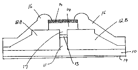
As shown in Figures 1 and 2, a discrete EAM comprises a base layer 10
having metalisation 19 and a connector 22 for making an external electrical
5 contact. The base layer 10 is formed of n-lnP with a mesa 11 which is 1200 nm
wide and 4200 nm high. An absorber region 13 is located on top of the mesa 1 1.
It is 260 nm thick and 800 nm wide and these dimensions mean that it is mono-
mode (i.e. only one principle mode is supported). It has a multi-quantum well
(MQW) structure formed of two different quaternary semiconductors having the
10 elements In, Ga, P and As in different proportions, There is a total of thirty one
layers, namely seventeen wells and sixteen barrier layers. The absorber region 13
has a higher refractive index than its surroundings and, as can more easily be seen
in Figure 2, it constitutes a path to guide optical signals from one end of the device
to the other. The length of the path is 400 ~m and it has anti-reflection coatings
15 23 and 24 on its two facets.
The absorber region 13 is covered with a cap 14 of p-lnP. The cap 14 is
6500 nm wide and 2900 nm thick with a downwardly extending projection 17
which is 500 nm long and 1200 nm wide. The projection 17 forms an interface
with the MQW 13. The cap 14 has external electrical contacts 15 comprising a
20 ternary layer of p-doped InGaAs and metalisation Ti/Au and a wire connector 21 is
attached to the Ti/Au.
The device includes an eiectrical blocking region 12a, 12b which is 5000
nm thick. It has a high resistance and it is formed of InP doped with Fe. The
electrical blocking region 1 2a, 1 2b is separated into two portions 12a and 12b by
25 the mesa 11, the MQW 13 and the projection 17. It is possible to make the
projection 17 longer than 500 nm with a lower mesa to compensate. For example,
if the projection 17 is increased to 2500 nm then the mesa should be reduced to
CA 02243279 1998-07-1~
W O 97/36204 PCT/GB97/00505
2240 nm if it is desired to keep the thickness of the MQW 13 at 260 nm and the
thickness of the electrical blocking layer 12 at 5000 nm. In any case. the height
of the electrical blocking region 12 is substantially equal to the sum of the heights
of these three items 11,13 and 17.
The thickness of the electrical blocking region 12 is a most important
feature of the invention and the absorber region 13 is in contact with the electrical
blocking region 12. In fact the absorber region 13 is between and in contact with
both portions 12a and 12b of the blocking region. It should also be noted that
with the absorber region 260 nm thick and the electrical blocking layer 5000 nm
thick, the electrical blocking region 12 is nearly 20 (1~.23) times thicker than the
absorber region
The electrical blocking region 12 is covered, on both sides, with a layer 16
of As doped glass to reduce the capacitance of the device.
Figure 3 shows a device as illustrated in Figures 1 and 2 located between
two optical fibres 30A and 30B. Fibre 30A has a core with a lens 31 A and a
cladding 32A. Fibre 30A provides input to the device. Fibre 30B has a core with a
lens 31B and a cladding 32B. Fibre 30B receives the output of the device. Rays
are focused on the absorber region 13 so that they are modulated and transmittedto the output fibre 30B. The lens 31B focuses light from the device so that it is
captured by the fibre 30B. There are air gaps between the two fibres 30A and
30B and the device and the anti-reflection coatings 23 and 24 are needed to
reduce the amount of light which is reflected.
Figure 4 shows a demultiplexer for four channels in optical time division
multiplex format. The demultiplexer comprises four EAM 45.1 - 45.4 each of
which is as shown in Figures 1 and 2. Each of the EAM selects one of the
channels and provides it to one of four optical detectors 46.1 - 46.4. The four
EAM receive electrical control signals from controller 44. The demultiplexer also
includes an erbium doped fibre amplifier (EDFA) 41. Each of the four channels
operates at a rate of 10 Gbit/s so that the total bit rate is 40 Gbit/s. These signals
are received on fibre 40 and amplified in the EDFA 41 to remove any attenuation
which has occurred in transmission. About 10 % of the signals are split onto fibre
42 and the remainder continue onto fibre 43. Fibre 42 is connected to the
controller 44 to synchronise the control signals. Controller 44 produces 4
CA 02243279 1998-07-1~ -
W O 97/36204 PCT/GB97/00505
electrical control signals which are phased at 90~ apart. And these are providedon connectors 47.1 - 47.4 to each of the EAM 45.1 - 45.4. The signals switch
the EAM so that each passes its own channel and blocks the others. The incoming
signals are divided into four equal parts on fibre 48. 1 - 48.4 so that each of the
5 EAM 45.1 - 45.4 receives the whole of the Incoming signals. Each EAM 45.1
45.4 also receives electrical control signals on connectors 47.1 - 47.4 with theresult that each of thc detectors 46.1 46.4 receives only one of the channels
whereby the ou~put consists of the demultiplexed channels.
It is emphasised that the arrangement shown in Figure 4 is conventional
10 for demultiplexers and Figure 4 illustrates that EAM according to the invention are
suitable for use in a conventional optical arrangement. It is also apparent thatintegral EAM cannot be used in arrangements such as Figure 4. Discrete EAM are
necessary and this invention relates to discrete EAM.
Several devices as described above were prepared and the average
15 modulation depth was 41 dB. Devices in which the electrical blocking region 12
was only 2500 nm thick had an average modulation depth of only 24 d8. In
addition the thinner electrical blocking region was associated with interferenceeffects during the "on" state.
While it is not intended to bè bound by any explanation, it is believed that,
20 using a mono-mode absorber region, EAM experience parasitic transmissions which
by-pass the intended transmission path. These transmissions are not affected (orare little affected) by the state of the modulator, but with a large blocking region
thickness the parasitic transmissions are not captured by the output fibre so the
adverse effects are not produced. In the "off" state the parasitic light represents
25 unwanted output. In the "on" state the parasitic light interferes with the intended
transmission. In the case of integral EAM there is no practical problem of parasitic
light because the laser and the EAM are closely integrated. Since both functionsare included on the same chip they are grown in the processing sequence using
common masks and the semiconductors have similar chemical compositions. Thus
30 the alignments are very accurate and the problems of parasitic light do not arise.