Note: Descriptions are shown in the official language in which they were submitted.
CA 02243305 1999-O1-27
SEI 98-20
T '
TITTE OF THE INVENTION
Optical Module for Receiving Optical Signal from
Optical Fiber
BACKGROUND OF THE INVENTION
Field of the Invent; nn
The present invention relates to an optical receiver
which converts an optical signal fed into a photodiode to
an electric signal.
Related Backgrn"nr~ Art
Fig. 14 shows a basic configuration of a conventional
optical receiver. An optical signal OS is converted into
its corresponding electric signal by a photodiode 1. Thus
formed photocurrent is converted into a voltage signal by
a preamplifier (transimpedance amplifier, current-voltage
converter circuit) 3 comprising an amplifier 3a and a
transimpedance 3b, and the resulting signal is transmitted
to a data-identifying/reproducing and clock-extracting
circuit 4.
It is often necessary for the conventional optical
receiver to monitor an average input light intensity.
Though the average value of the photocurrent generated in
the photodiode has to be detected therefor, no circuit for
this purpose can be inserted in the anode of the photodiode
1. This is because the preamplifier 3 is connected to the
anode of the photodiode 1 and, consequently, another circuit
element connected thereto would deteriorate waveforms of
1
CA 02243305 2002-07-04
signals, in particular, in high-frequency bands used for
optical signal transmission.
SUMMARY OF THE :INVENTION
The optical receiver in accordance with one embodiment
of the present .invention comprises a photodi.ode for
receiving an optical signal emitted from an optical fiber;
a current mirror r_ircuit having two parallel. lines with
respective currents flowing therethrough at levels in
proportion to each other, one of the lines being connected
to one end of the photodiode; and a t;ransimpedance
amplifier connected to the other end ofthe photodiode.
In another embodiment, the present: invention provides
an optical receiver comprising a phot:odi.ode configured and
arranged to receive an optical signal emitted from an
IS optical fiber, a current mirror <;ircuit. connected to one
end of the photodiode, a transimpedance amplifier connected
to the other end of the photodiode, a package having the
photodiode, the current mirror circuit and the
transimpedence amplifier arranged therein, a position
fixing member attaching the optical fiber to the package,
and a support member arranged in the package, supporting
both of the phot;odiode and the transi.mpedance amplifier,
wherein the current mirror circuit has first and second
n-channel field-effect transistors, the transistors having
CA 02243305 2002-07-04
their respective gates connected to the other transistor's
source.
In this optical receiver, in tl:~: case where the
photodiode is cathode-grounded, since the current. mirror
circuit is provided, the photocurrent flowing into the
photodiode can be amplified by the transimpedance amplifier
and observed as a current, flowing out of the photodiode by
way of the other line. In the case where the photodiode is
anode-grounded, since the current mix:ror circuit is
provided, the photocurrent flowing out of the photodiode
can be amplified by the transimpedance amplifier and
observed as a current flowing into the photodiode by way of
the other line.
Preferably, the optical receiver in accordance with
the present invention further comprises a resin material
for molding the transimpedarlce amplifier or current mirror
circuit.
2a
CA 02243305 1999-O1-27
SEI 98-20
The present invention will become more fully understood
from the detailed description given hereinbelow and the
accompanying drawings which are given by way of illustration
only, and thus are not to be considered as limiting the
present invention.
Further scope of applicability of the present invention
will become apparent from the detailed description given
hereinafter. However, it should be understood that the
detailed description and specific examples, while
indicating preferred embodiments of the invention, are
given by way of illustration only, since various changes
and modifications within the spirit and scope of the
invention will become apparent to those skilled in the art
from this detailed description.
I5 BRT .F D .S RT TTnN O TH D AWTNCS
Fig. 1 is a perspective view showing an optical module
10 in accordance with a first embodiment;
Fig. 2 is a sectional view of the optical module 10
taken along the arrowed line II-II of Fig. 1;
Fig. 3 is a circuit diagram of the optical module in
accordance with the above-mentioned embodiment;
Fig. 4 is a circuit diagram including a monitor circuit
13;
Fig. 5 is a circuit diagram showing a modified example
of transimpedance amplifier 3;
Fig. 6 is a circuit diagram of an optical module in
3
CA 02243305 1999-O1-27
SEI 98-20
accordance with a second embodiment;
Fig. 7 is a circuit diagram of an optical module in
accordance with a third embodiment;
Fig. 8 is a circuit diagram of an optical module in
accordance with a fourth embodiment;
Fig. 9 is a sectional view of an optical module in
accordance with a fifth embodiment;
Fig. 10 is a sectional view of an optical module in
accordance with a sixth embodiment;
Fig. 11 is a sectional view of an optical module in
accordance with a seventh embodiment;
Fig. 12 is a sectional view of an optical module in
accordance with an eighth embodiment;
Fig. 13 is a sectional view of an optical module in
accordance with an ninth embodiment; and
Fig. 14 is a circuit diagram showing a basic
configuration of a conventional optical receiver.
In the following, optical modules in accordance with
embodiments will be explained. Constituents identical to
each other or those having functions identical to each other
will be referred to with numerals or letters identical to
each other without repeating their overlapping explanations.
Also, the following embodiments will be explained only in
terms of their distinguishable constituents in cases where
there are identical constituents among them.
4
CA 02243305 1999-O1-27
SEI 98-20
First Embodiment
Fig. 1 is a perspective view showing an optical module
in accordance with the first embodiment.
The optical module 10 comprises a resin material
5 (resin package) l0a assembled with assembling members; a
plurality of lead terminals lOc drawn out of the resin
material 10a; and a boot member BT holding an end portion
of an optical fiber OF and projecting from one side face
(hereinafter referred to as front face) of a tip part of
10 the resin material 10a.
Fig. 2 is a sectional view of the optical module 10
taken along the arrowed line II-II of Fig. 1. Embedded
within the resin material l0a is a sleeve SV in which an
optical fiber OF surrounded by the ferrule lOd is disposed.
The ferrule lOd is a cylindrical shell comprising a
cylindrical inserting portion for inserting the end portion
of the optical fiber OF therein.
The end face of the optical fiber OF within the sleeve
SV faces a photodiode 1 via a lens LS, the photodiode 1 being
fixed to the inside of a support member SM, the support member
SM attached to one end of the opening of the sleeve SV via
a connecting member CM. The support member SM functions as
a lid of a can-type package of the photodiode 1. The sleeve
Sv and connecting member CM constitute a position fixing
member that attaches optical fiber OF to the package 10a.
The photodiode 1 is electrically connected to a
5
CA 02243305 1999-O1-27
SEI 98-20
current mirror circuit 2 and a transimpedance circuit 3 which
is connected to a data-identifying/reproducing and
clock-extracting circuit 4.
In this embodiment, the current mirror circuit 2, the
transimpedance circuit 3, and the circuit 4 are disposed
on a wiring board (lead-frame) 5, and are molded and embedded
within the resin material 10a.
Fig. 3 is a circuit diagram of the optical module in
accordance with this embodiment. The current mirror
circuit 2 is constituted by a pnp transistor 2a whose
collector and base are short-circuited therebetween and a
pnp transistor 2b substantially identical thereto in terms
of characteristics. The respective bases of these two
transistors 2a, 2b are connected in common, whereas their
emitters are commonly connected to a positive power supply
Vcc. The transistors 2a and 2b have characteristics nearly
identical to each other and are disposed close to each other
on the same board 5, thereby operating under the same
environment. These transistors may also be fabricated on
the same semiconductor chip.
The collector of the transistor 2a is connected to the
cathode of the photodiode 1, whereas the anode of the
photodiode 1 is connected to the data-
identifying/reproducing and clock-extracting circuit 4 by
way of the transimpedance amplifier 3.
The photodiode 1 is a light-receiving device which
6
CA 02243305 1999-O1-27
SEI 98-20
receives an optical signal incident thereon and outputs a
current signal corresponding to the quantity of light of
this optical signal. For example, as a semiconductor
light-receiving device, a PIN photodiode having a diameter
of 50,um made of InGaAs is preferably used. The optical
signal received by the photodiode 1 is signal light
containing data in a predetermined cycle. This signal can
transmit data, in synchronization with a clock signal, at
a bit rate (e. g., 2.4 Gb/s) corresponding to the above-
mentioned cycle.
The transimpedance amplifier 3 converts the
photocurrent generated in the photodiode 1 into its
corresponding voltagesignal. Preferably employable as the
transimpedance amplifier 3 is, for example, an amplifier
circuit comprising an amplifier made of GaAs and a feedback
resistance element connected between the input and output
thereof.
The collector potential of the transistor 2a is a
potential lower than the positive power supply Vcc by the
base-emitter voltage of the transistor 2a. This base-
emitter voltage equals the forward clamping voltage of the
diode and is set to about 0.7 to 0.8 V under normal operating
conditions of the transistor 2a. As a consequence, the
cathode potential of the photodiode 1 becomes Vcc - (0.7
to 0.8) V, whereby a sufficient reverse bias voltage is
applied to the photodiode 1 . Since the base-emitter voltage
7
CA 02243305 1999-O1-27
SEI 98-20
of the transistor 2b perfectly equals the base-emitter
voltage of the transistor 2a, the current flowing out of
the collector of the transistor 2b is made equal to the
current flowing into the cathode of the photodiode 1. The
collector of this transistor 2b can be utilized as an input
terminal of a monitor circuit for a monitoring the
photocurrent, i.e., a photocurrent monitor terminal MT.
Fig. 4 is a circuit diagram including a monitor circuit
13 mentioned above. The monitor circuit 13 comprises a
current-voltage converter circuit 13 constituted by an
operational amplifier (Op-Amp) 13a1 and a transimpedance
13b1.
Connected between an inverting input terminal 13a2 and
an output terminal 13a, of the Op-Amp 13a1 is a resistor 13b1
for current-voltage conversion. Connected to a
noninverting input terminal 13a, of the Op-Amp 13a1 is a bias
power supply Vb. In this circuit, when the photocurrent
monitor terminal MT is connected to the inverting input
terminal 13a2, the current equivalent to the photocurrent
lp flowing out of the collector of the transistor 2b does
not flow into the input of the Op-Amp 13a1 but mostly appears
at the output terminal by way of the resistor 13b1. Due to
the feedback effect of the resistor 13b1, the Op-Amp 13a1
operates such as to hold the potential between its two input
terminals at zero, whereby the potential of the inverting
input terminal l3az of the Op-Amp 13a1 is made equal to the
8
CA 02243305 1999-O1-27
SEI 98-20
potential Vb of the noninverting input terminal 13a,. A
voltage of (Vb - lp X R) is hence generated at the output
terminal, whereby the photocurrent can be detected by
monitoring this voltage.
When a resistor is inserted between the emitter of at
least one of the transistors 2a and 2b and the positive power
supply Vcc, the sum of the base-emitter voltage of one of
the transistor to which the resistor is inserted and the
voltage decrease at thus inserted resistor equals the
base-emitter voltage of the other transistor to which the
resistor is not inserted, whereby the level of monitor
current lp can be changed while the ratio between the
respective currents flowing through both transistors is
held constant.
For example, when a resistor is inserted between the
emitter of the transistor 2a and the positive power supply
Vcc, the base-emitter voltage of the transistor 2b becomes
greater than the base-emitter voltage of the transistor 2a.
Consequently, the level of monitor current lp can be made
greater than the level of photocurrent actually flowing into
the photodiode 1. On the other hand, when a resistor is
inserted between the emitter of the transistor 2b and the
positive power supply Vcc, while the emitter of the
transistor 2a is directly connected to the positive power
supply Vcc, the level of monitor current lp can be made
smaller than the photocurrent. Namely, the current mirror
9
CA 02243305 1999-O1-27
SEI 98-20
circuit has two parallel lines with respective currents
flowing therethrough at levels in proportion to each other,
while one of the lines is connected to one end of the
photodiode.
Fig. 5 shows a modified example of the transimpedance
amplifier 3. This optical module can employ, in place of
the transimpedance amplifier 3, a current-voltage converter
circuit 3' consisting of a resistor 3b' shown in Fig. 5.
Second Embodiment
Fig. 6 shows a circuit diagram of an optical module
in accordance with the second embodiment. The
configuration thereof not depicted here is identical to that
of the first embodiment. Depicted current mirror circuit
2 is constituted by an npn transistor 2a whose collector
and base are short-circuited therebetween and an npn
transistor 2b substantially identical thereto in terms of
characteristics. The respective bases of these two
transistors 2a, 2b are connected in common, whereas their
emitters are commonly connected to a negative power supply
Vee. The transistors 2a and 2b have characteristics nearly
identical to each other and are mounted close to each other,
thereby operating under the same environment. These
transistors may also be fabricated on the same semiconductor
chip.
The collector of the transistor 2a is connected to the
anode of a photodiode 1, whereas the cathode of the
CA 02243305 1999-O1-27
SEI 98-20
photodiode 1 is connected to a data-identifying/reproducing
and clock-extracting circuit 4 by way of a transimpedance
amplifier 3. The transimpedance amplifier 3 converts a
photocurrent generated in the photodiode 1 into a voltage
signal corresponding thereto. As a consequence of this
configuration, the collector potential of the transistor
2a is a potential higher than the negative power supply Vee
by the base-emitter voltage of the transistor 2a. This
base-emitter voltage equals the forward clamping voltage
of the diode. Under normal operating conditions of the
transistor 2a, the clamping voltage is set to about 0.7 to
0.8 V. As a consequence, the anode of the photodiode 1
attains a potential of Vee + (0.7 to 0.8) V, whereby a
sufficient reverse bias voltage is applied to the photodiode
1. Since the base-emitter voltage of the transistor 2b
perfectly equals the base-emitter voltage of the transistor
2a, the current flowing into the collector of the transistor
2b is made equal to the current flowing out of the anode
of the photodiode 1. Hence, the collector of this
transistor 2b can be utilized as a photocurrent monitor
terminal MT.
The npn transistor shown in Fig. 6 may be replaced by
n-channel field-effect transistors (n-FETs). Namely, in
this case, the respective gates of two n-FETs having
substantially the same characteristics are connected
together, and the drain and gate of one FET are short-
11
CA 02243305 1999-O1-27
~ SEI 98-20
circuited therebetween, whereas the anode of the photodiode
1 is connected to the drain of this FET. The photocurrent
flowing out of the photodiode 1 can be monitored by observing
the current flowing into the drain of the other FET.
Th i__rd Embod i m nt-.
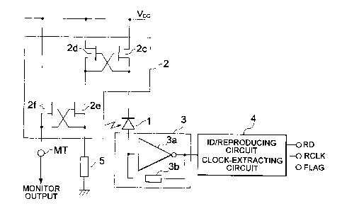
Fig. 7 shows a circuit diagram of an optical module
in accordance with the third embodiment . The configuration
thereof not depicted here is identical to that of the first
embodiment . This optical module is an example in which the
current mirror circuit 2 for the current flowing out of the
positive power supply side is constituted by n-channel FETs
2c, 2d, 2e, and 2f. The anode of a photodiode 1 is connected
to a transimpedance amplifier 3. The gates and sources of
the n-FETs 2c and 2d are connected to each other in a crossing
fashion, whereas their drains are connected to a positive
power supply Vcc. The source of the n-FET 2c is connected
to the cathode of the photodiode 1, whereas the source of
the n-FET 2d is connected to the drain of the FET 2e in a
circuit constituted by the n-FETs 2e and 2f whose gates and
sources are connected to each other in a crossing fashion.
The drain of the FET 2f is connected to the positive power
supply Vcc.
The n-FETs 2c to 2f have substantially the same
characteristics and are mounted close to each other, thereby
operating under the same condition. They may also be
fabricated on the same semiconductor chip. For monitoring
12
CA 02243305 1999-O1-27
' SEI 98-20
the photocurrent generated in the photodiode 1, it is
possible to employ not only a method in which the current
flowing into the photodiode 1 from the positive power supply
side is observed but also a method in which the current
flowing out of the n-FET 2f is observed by way of a monitor
terminal MT.
Employable as the above-mentioned n-FETs are GaAs-
MESFET, Si-n-channel MOSFET, Si-n-channel JFET, and the
like.
FoL_rth Embodimen
Fig. 8 shows a circuit diagram of an optical module
in accordance with the fourth embodiment. The
configuration thereof not depicted here is identical to that
of the first embodiment. Though the current mirror circuit
2 in each of the above-mentioned embodiments is preferably
incorporated within the optical module, it can be disposed
outside the optical module. In this case, the distance in
wiring between the current mirror circuit 2 and the
photodiode 1 becomes long. In such a case, since noise is
likely to be superposed on the long wiring, a capacitor C
is disposed in parallel to the wiring line connecting the
current mirror circuit 2 and the photodiode 1. The
capacitor C is disposed near the photodiode 1 or within the
resin material 10a. The capacitor C is connected between
the wiring line and the ground, thereby improving the
resistance of photocurrent to noise. Here, even when the
13
CA 02243305 1999-O1-27
~ SEI 98-20
current mirror circuit 2 is not disposed outside the optical
module, the circuit of Fig. 8 may be used when the wiring
line is long.
Fifth Embodiment
Fig. 9 shows a sectional view of an optical module in
accordance with the fifth embodiment. The configuration
thereof not depicted here is identical to that of the first
embodiment. In the fifth embodiment, the transimpedance
amplifier 3 in the optical module described in the
above-mentioned first to fourth embodiments is fixed to a
surface of the support member SM, the surface facing the
end of the optical fiber OF. In this case, since the
transimpedance amplifier 3 and the photodiode 1 can be
disposed close to each other, the noise superposed on the
wiring therebetween can be reduced.
Sixth Embodiment
Fig. 10 shows a sectional view of an optical module
in accordance with the sixth embodiment. The configuration
thereof not depicted here is identical to that of the first
embodiment. In the optical module of the sixth embodiment,
the current mirror circuit 2 in the optical module described
in the above-mentioned first to fourth embodiments is fixed
to the surface of the support member SM, the surface facing
the end of the optical fiber OF. In this case, since the
current mirror circuit 2 and the photodiode 1 can be disposed
close to each other, the noise superposed on the wiring
14
CA 02243305 1999-O1-27
' ' SEI 98-20
therebetween can be reduced.
Seventh Embodiment
Fig. 11 shows a sectional view of an optical module
in accordance with the seventh embodiment. The
configuration thereof not depicted here is identical to that
of the first embodiment. In the optical module of the
seventh embodiment, the current mirror circuit 2 and
transimpedance amplifier 3 in the optical module described
in the above-mentioned first to fourth embodiments are fixed
to the surface of the support member SM, the surface facing
the end of the optical fiber OF. In this case, since the
photodiode 1, the current mirror circuit 2, and the
transimpedance amplifier 3 can be disposed close to each
other, the noise superposed on the wiring therebetween can
be reduced.
Eighth Embodiment
Fig. 12 shows a sectional view of an optical module
in accordance with the eighth embodiment. The
configuration thereof not depicted here is identical to that
of the fourth embodiment. In the optical module of the
eighth embodiment, the current mirror circuit 2 in the
optical module described in the fourth embodiment is
disposed outside the optical module. Though the distance
between the current mirror circuit 2 and the photodiode 1
is elongated, a capacitor C connected between the wiring
line and the ground as shown in Fig. 8 can improve the
CA 02243305 1999-O1-27
SEI 98-20
resistance of photocurrent to noise.
Fig. 13 shows a sectional view of an optical module
in accordance with the ninth embodiment. The configuration
thereof not depicted here is identical to that of the eighth
embodiment. The only difference from the module in Fig. 12
is that the transimpedance amplifier 3 is fixed to the inner
surface of the support member SM.
As explained in the foregoing, since the current
mirror circuit 2 is provided in the optical receivers in
accordance with the above-mentioned embodiments, when the
photodiode 1 is cathode-grounded, the photocurrent flowing
into the photodiode 1 can be observed as a current flowing
out of the photodiode 1. When the photodiode 1 is
anode-grounded, since the current mirror circuit 2 is
provided, the photocurrent flowing out of the photodiode
1 can be observed as a current flowing into the photodiode
1. Hence, tolerance can be remarkably enhanced in the
circuit configuration of the monitor circuit 13.
A monitoring method to be compared with the system of
the above-mentioned embodiments will now be explained. In
this method, a current-detecting circuit and a photodiode
are connected in series. In order to set a high
photoelectric conversion efficiency in the photodiode, it
is necessary to provide a sufficient potential difference
between both terminals of the photodiode. On the other hand,
16
CA 02243305 1999-O1-27
' SEI 98-20
r
the current-detecting circuit would not function normally
unless a predetermined potential is set therein. Thus,
there are various restrictions on detecting the average
value of photocurrent at the cathode terminal of the
photodiode. The average photocurrent flowing out of the
photodiode is detected by a current-detecting means
inserted between the anode of the photodiode and a negative
power supply. Here, the circuit would not operate normally
unless a sufficient bias is applied to both of the photodiode
and the current-detecting means, either. The system in
accordance with the above-mentioned embodiments has an
advantage over the method in which a current-detecting
circuit is inserted between the cathode of the photodiode
and a positive bias terminal so as to detect the average
value of photocurrent flowing into the photodiode. The
optical receiver in accordance with any of the above-
mentioned embodiments can supply a sufficient bias
potential to the photodiode 1 so that its photoelectric
conversion efficiency would not decrease, while the
photocurrent of the photodiode can be monitored
sufficiently. Also, since monitoring can be effected
without affecting characteristics of the photodiode 1, the
monitor circuit can be designed easily.
From the invention thus described, it will be obvious
that the invention may be varied in many ways. Such
variations are not to be regarded as a departure from the
17
CA 02243305 1999-O1-27
SEI 98-20
spirit and scope of the invention, and all such
modifications as would be obvious to one skilled in the art
are intended for inclusion within the scope of the following
claims.
18