Note: Descriptions are shown in the official language in which they were submitted.
- . CA 02243803 1998-07-23
PATENT P-3701
TITLE OF THE INVENTION
A CIRCUIT FOR CAUSING A VOLTAGE STEP IN A MULTI-CELL BATTERY
FIELD OF THE INVENTION
The present invention generally relates to circuits and
batteries, and more specifically relates to a circuit for
causing a voltage step in a battery comprising a plurality of
serially-connected cells useful in iontophoretic drug delivery
systems for delivering drugs or medicines to patients
transdermally, i.e., through the skin In a preferred
embodiment of the present invention, this voltage-step causing
circuit is employed by a controller of the iontophoretic drug
delivery system.
BACKGROUND OF THE INVENTION
The output voltage of the battery is often used as an indicator
of the energy remaining in the battery. That output voltage
may be monitored by a voltage monitoring circuit, either
internally connected to the device to which the battery
supplies energy or externally connected to that device. The
output voltage of some types of batteries, such as alkaline
manganese dioxide Zn/MnO2 batteries (hereinafter referred to as
'alkalinell batteries) gradually decreases, as shown in Fig. lA
(corresponding to Fig. 7.5 of the Handbook of Batteries, edited
by David Linden, 1984). When the monitoring circuit has
detected that the output voltage has decreased below a
predetermined voltage level, there might be enough energy left
in the battery for the device to complete a critical ongoing
task, such as drug delivery in an iontophoretic drug delivery
system, as described below, or to perform an essential power-
, CA 02243803 1998-07-23
t
down function, such as memory backup in a battery-powered
computer. These types of batteries, however, may not be
preferred for certain applications which require batteries with
high energy and high current capacity.
Other conventional batteries, such as zinc/silver oxide
batteries (Zn/Ag2O, hereinafter referred to a "silver oxide
batteries"), are characterized by a substantially flat output
voltage over time, until the cells of the battery die, at which
time the output voltage sharply decreases, as shown by Fig. lB
(corresponding to Fig. 9.4 of the Handbook of Batteries).
Despite this discharge characteristic, silver oxide batteries
are preferred for certain electrical applications because they
are small, thin and light, and deliver a high amount of current
for a long period of time. When the voltage monitoring circuit
has detected that the output voltage of the battery has begun
to decrease sharply, there may not be enough energy left in the
battery, however, for the device to complete a critical ongoing
task or to perform an essential power-down function.
Therefore, there is a need for a high quality, high-current
delivering battery, such as the conventional silver oxide
battery, which also has enough r~m~;n;ng energy, after the
voltage monitoring circuit has detected the sharp decrease in
the output voltage, to allow the device to complete its task or
to power-down.
Section 8.5.7 of the Handbook of Batteries describes a
"stepped-voltage" battery which produces a well-defined step in
the output voltage prior to its complete discharge, as shown in
Fig. lC (corresponding to Fig. 8.25 of the Handbook of
Batteries). This voltage step occurs well before the end of
battery life so that, after the voltage monitoring circuit has
detected the voltage step, enough energy r~m~;n~ in the battery
CA 02243803 1998-07-23
to allow the device to complete a final task or to power-down.
The stepped-voltage battery is made by using materials in the
cathode or the anode of the battery which discharge at a
different potential from the base electrode.
In particular, Fig. lC shows a nine-cell battery having a
stepped battery voltage discharge curve Vtotall which is
produced by serially connecting seven zinc/mercuric oxide cells
that together are characterized by the substantially flat
voltage discharge curve V2, and two hybrid cells that together
are characterized by the stepped voltage discharge curve Vl.
The hybrid cells have cathodes in which part of the mercuric
oxide has been replaced by cadmium oxide in a sufficient
quantity to leave each hybrid cell with the same balanced
capacity. When all of the mercuric oxide has been reduced in
the hybrid cells, that is, the hybrid cells have discharged,
their combined voltage falls by 1.5 Volts (750 millivolt per
hybrid cell), as shown in curve Vl. This causes the combined
voltage Vtota1 to decrease by 1.5 Volts. This sudden, large
drop in the output voltage can be easily detected by the
voltage monitoring circuit, and thus can serve to trigger an
alarm indicating the need for battery replacement, or to warn
the device that any ongoing task should be a final task or that
the device should begin powering down. The size of the voltage
step can be adjusted, for example, by increasing or decreasing
the number of hybrid cells in the battery. Further, during
manufacture of the stepped-voltage battery, the voltage step
can be arranged to occur at varying points during the life of
the battery. For example, in the nine-cell battery of Fig. lC,
the voltage step was arranged to occur at about 60~ (650 hours)
of the overall life (1100 hours).
The above-described stepped-voltage batteries are, however,
CA 02243803 1998-07-23
limited in their use, especially as a substitute for silver
oxide batteries and the like. First, all the cells of the
stepped-voltage battery are arranged in a relatively large,
wide and heavy package, making its use impractical for small or
thin electronic devices. Second, relative to silver oxide
batteries, stepped-voltage batteries are expensive and have a
lower current capacity. Third, to meet all of the different
energy requirements of various devices, a device manufacturer
would need to order and stock, unfortunately, many different
~ 10 types of stepped-voltage batteries. Finally, although the time
at which the voltage step of the stepped-voltage battery occurs
can be set as described above, that setting is set during
manufacturing and cannot be adjusted thereafter. It would be
more desirable to be able to use a battery with which the time
of the voltage step can be adjusted while the device is being
operated. Such time adjustment can be based on the operating
conditions of the device using, for example, computer control.
~hus, despite the availability of stepped-voltage batteries,
there is still a need for a time-adjustable, stepped-voltage
output when use of a more practical and desirable conventional
battery, such as a silver oxide battery, is required by the
device.
SUMMARY OF THE INVENTION
In contrast to the above, it has been found that a circuit
advantageously causes a voltage step in a battery of a
plurality of serially-connected cells so that the voltage step
may be detected and acted upon is particularly suited for use
in connection with the iontophoretic delivery of the drug,
medicament or the like. In addition, the circuit causes one
(or more) of the cells to discharge through a resistor at a
CA 02243803 1998-07-23
higher rate than the other cells, thus producing a voltage step
when the faster discharging cell dies before the other cells.
A reverse-biased diode is connected in parallel to the faster
discharging cell to cause the current to bypass the faster
discharging cell after it has discharged, thus preventing that
cell from reverse charging. This circuit may be controlled to
adjust the time of occurrence of the voltage step.
In another aspect of the present invention, another diode is
connected in series with the resistor to prevent the other
cells from discharging through the resistor if the battery is
connected to a push-pull switch in the device.
In yet another aspect of the present invention, multiple
resistor and diode circuits are added to provide multiple
voltage steps.
BRIEF DESCRIPTION OF THE DRAWINGS
The various features, objects, benefits, and advantages of the
present invention will become more apparent upon reading the
following detailed description of the preferred embodiment
along with the appended claims in conjunction with the
drawings, wherein like reference numerals identify
corresponding components, and:
Figure lA depicts a battery discharge curve for a conventional
alkaline battery.
Figure lB depicts a battery discharge curve for a conventional
silver oxide battery.
Figure lC depicts a battery discharge curve for a conventional
CA 02243803 1998-07-23
stepped-discharge battery.
Figures 2A and 2B depict the iontophoretic drug delivery system
of the present invention.
Figures 3A-3C depict circuits in accordance with a first
embodiment of the present invention.
Figure 4A depicts a voltage monitoring circuit used with the
present invention.
Figure 4B depicts an illustrative output voltage curve for the
voltage monitoring circuit shown in Figure 4A.
Figures 5A and 5B depict output voltage curves in accordance
with the first embodiment of the present invention.
Figure 6 depicts a circuit in accordance with a second
embodiment of the present invention.
Figure 7 depicts a circuit in accordance with a third
embodiment of the present invention.
DETAILED DESCRIPTION OF THE PREFERRED EMBODIMENTS
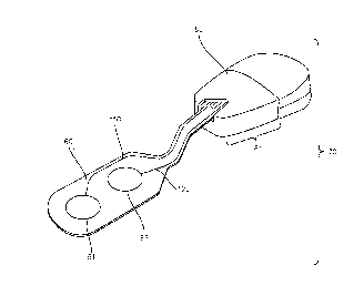
The iontophoretic drug delivery system 70 of the present
invention is illustrated in Figures 2-7, with the controller
generally designated 80 and the patch generally designated 60.
Conventional iontophoretic devices, such as those described in
U.S. Patent Nos. 5,498,235 (Flower), 5,540,669 (Sage, Jr. et
al.), and 5,645,526 (Flower), the disclosures of which are
hereby incorporated by reference, for delivering a drug or
medicine transdermally through iontophoresis, basically
CA 02243803 1998-07-23
consist of two electrodes, which are in contact with a portion
of a patient's body. A first electrode, generally called the
active electrode, delivers the ionic substance or drug into
the body by iontophoresis. The second electrode, generally
called the counter electrode, closes an electrical circuit
that includes the first electrode and the patient's body.
Generally, the circuit includes a source of electrical energy,
such as a battery. The ionic substance to be driven into the
body may be either positively charged or negatively charged.
In the case of a positively charged ionic substance, the anode
of the iontophoretic device becomes the active electrode and
the cathode serves as the counter electrode to complete the
circuit. Alternatively, if the ionic substance to be
iontophoretically delivered is negatively charged, the cathode
will be the active electrode and the anode will be the counter
electrode.
Referring to Figures 2A and 2B, the controller 80, including
the battery, is respectively connected to an anode 61 and
cathode 62 in the patch 60 via the electrical interconnectors
110 and 120. The controller 80 includes an outer casing 81
which houses the power source and current generation and
regulation circuitry required for driving current into the
patch 60. The casing of the controller 80 may be made of a
plastic, metal or other suitable material for encasing and
protecting the current regulating circuitry. The patch
electrodes 61 and 62 electrically connect to the current
controller 80 via electrical connectors 110 and 120.
The anode 61 is arranged in the active reservoir containing a
positively-charged drug, while the cathode 62 is arranged in
the return reservoir cont~;n;ng the electrolytic (or saline)
solution. If the drug is negatively-charged, the anode and
CA 02243803 1998-07-23
cathode arrangement in the reservoirs is reversed, so that when
current is applied to the electrodes, drug ions will be
repelled from the reservoir of similar polarity. When the
patch 60 is placed on the skin of a user and the controller
applies current to the patch 60, the charged drug is forced
into the skin and blood of the patient. Ions charged
oppositely of the drug ions are returned to the return
reservoir as the body completes the iontophoretic circuit. For
example, if the drug is negatively-charged, a AgCl cathode will
~ 10 repel them through the skin and into the blood vessel, while
positively-charged sodium ions are attracted to the cathode.
At the same time, negatively-charge chlorine ions will flow
from the skin into the return reservoir containing saline
toward the anode.
The controller 80 usually includes a microprocessor or state
machine to implement the numerous control functions. For
example, a microprocessor executes software programs which,
inter alia, command the current generation and regulation
circuitry to provide the required amount of current over a
period of time. Because the amount of drug delivered to the
patient is directly proportional to the amount of current
delivered, the drug dosage can be controlled by regulating the
amount of current delivered to the patch. As shown in more
detail in Figure 2B, the controller 80 includes the
microprocessor 20, which upon execution of software, generates
comm~n~ to control the various functions of the controller,
including but not limited to generating and regulating the
current applied to the patch as dictated by a predetermined
current delivery profile. To accomplish these functions, the
microprocessor 20 is connected to the current generation and
regulation circuitry, including digital interface and control
circuit 30, analog current control circuit 50 and peripheral
CA 02243803 1998-07-23
current control circuitry 40. The peripheral current control
circuitry 40 applies the current to the patch 60. The
microprocessor 20, digital interface 30, and analog control
circuitry 50, together with a memory 10 described in detail
below, may comprise an application specific integrated circuit
(ASIC). The peripheral current control circuitry 40 is called
"peripheral" because it is outside the ASIC. Of course, it
will be appreciated that the current generation and regulation
circuitry may take on other configurations, and need not be
implemented by an ASIC.
The microprocessor 20 is also connected to at least one memory
10 such as random access memory (RAM) or a read-only memory
(ROM), in which are stored the current delivery profiles. The
controller software may also be stored in the same memory or a
separate memory (not shown). The memory 10 may store, for
example, each current delivery profile as rate of change of
current (di/dt), or current steps, and the time after start-up
at which those current steps are to occur. The microprocessor
reads the current delivery profile information to generate the
appropriately timed commands required to cause the current
generation and regulation circuitry to deliver the amount of
current dictated by the profile information. In essence, the
microprocessor may cycle through the current profile
information until the time after start-up matches one of the
stored times. At that time, the microprocessor outputs the
desired current level, as a digital value, associated with that
time to the digital interface of the current circuitry. The
digital interface, which includes a digital to analog
convertor, converts the digital value to an analog voltage,
which will be that voltage required to produce the current
level at that point in time of the current delivery profile.
The D/A convertor outputs the analog voltage to a voltage-to-
CA 02243803 1998-07-23
current conversion circuit, which generates the required patch
current. Feedback from a sensor, such as a current sense
resistor, may be used to control the patch current more
precisely.
As stated above, there is a need for a circuit which causes a
step in the battery voltage output which can be detected by a
voltage monitoring circuit so as to allow the iontophoretic
drug delivery system to complete a drug delivery cycle. The
first embodiment of the present invention, preferably
implemented in the current controller 80, relates to the
circuit illustrated in Figure 3A. In Figure 3A, C1 and C2 are
serially-connected cells that altogether form a battery. Cl
and C2 may each comprise one of more individual cells, but for
simplicity, will hereinafter be designated as "battery Cl" and
"battery C2". Each individual cell of battery Cl or battery C2
may be of any compatible electrochemistry type and may be of
any voltage. For example, battery C1 may be a single 1.5 Volts
silver oxide cell and battery C2 may be three serially-
connected 1.5 Volts silver oxide cells, for a total outputvoltage (Vcl + Vc2), when fully charged, of 6.0 Volts.
Moreover, each cell in battery C2 may be individually packaged,
or all the cells of battery C2 may be arranged in a single
package. All of the cells comprising either battery C1 or C2
are electrically connected anode (positive terminal) to cathode
(negative terminal), as in any standard serial connection.
In this circuit, battery C1 is discharged at a higher rate than
battery C2, and thus battery C1 will completely discharge
before battery C2. This will cause a discernible step in the
output voltage across lines A and C, which can be detected by
the voltage monitoring circuit shown in Figure 4A. The
detection of the voltage step can be used as an indication that
- 10
CA 02243803 1998-07-23
any ongoing task should be the final task attempted by the
device, or as a trigger to begin powering down or any other
device function. At that time, battery C1 will be bypassed by
diode D1 to prevent it from reverse charging, and battery C2
should have sufficient energy to complete any ongoing task or
to power-down. Moreover, the voltage step detection can be
used to alert the user of the device that the batteries C1
and/or C2 need replacement or recharging, or if the device is
disposable that the device should be discarded, after
completion of the final task or power-down.
The circuitry for discharging battery C1 at a higher rate than
battery C2 comprises diode D1 and resistor R1, as shown in
Figure 3A. One terminal of resistor R1 is connected to the
anode of battery C1, and the other terminal of resistor R1 is
connected to one terminal of switch SW via line B. The order
of the resistor R1 and switch SW may be reversed. The anode of
diode D1 is connected to the cathode of battery C1, and the
cathode of diode D1 is connected to the anode of battery C1,
that is, diode D1 is reverse-biased with respect to battery C1
when battery C1 is charged. The voltage monitoring and device
circuitry is connected to the cathode of battery C1 via line A
and the anode of battery C2 via line C. Line A is also
connected to the other terminal of switch SW. Switch SW may be
part of the device circuitry, and is preferably a MOSFET
transistor, the gate of which is under microprocessor control
(not shown). Closing switch SW connects line B to line A.
Operation and Use
Having described one embodiment of the iontophoretic drug
delivery system, including the controller 80 and the patch 60,
of the present invention, its operation and use is described
CA 02243803 1998-07-23
below.
Specifically, the device circuitry of Figure 3A causes a higher
rate of discharge in battery C1 by closing switch SW and
connecting line B to line A. Thus, while both batteries C1 and
C2 discharge through the device circuitry and voltage
monitoring circuitry, battery C1 additionally discharges
through resistor R1. Closing of switch SW is preferably
performed under computer control by means well known in the
- 10 art. When battery C1 is fully or substantially charged, diode
D1 is reverse-biased with respect to battery C1 and thus acts
an open-circuit. The equivalent circuit of this operational
state is shown in Figure 3B. The output voltage across lines C
and A is shown in Figure 5A, and the voltage across lines B and
A is shown in Figure 5B.
As stated above, both batteries C1 and C2 will eventually
discharge over time, but because of the additional discharge of
battery C1 through resistor R1, battery C1 will completely
discharge before battery C2, as shown in Figure 5A (battery Cl
dies at about 9.4 hours when R1 = 600 ohms). When battery C1
is completely discharged, it will begin to reverse charge and
its voltage becomes a negative value, as shown in Figure 5B.
Diode Dl is now forward-biased with respect to battery Cl and
begins to conduct, and the current bypasses battery C1. The
device circuitry also disconnects lines A and B via switch SW
because there is no longer any need to discharge battery Cl,
resulting in the equivalent circuit shown in Figure 3C. The
voltage applied to the device circuitry is now VC2 - VD1 (VD11
for example, is about 0.7 Volts). In the example shown in the
output voltage curve of Figure 5A, the output voltage drops
from approximately 5.6 Volts to 3.8 Volts when battery Cl dies.
This voltage drop causes an easily detectable voltage swing in
- 12 -
CA 02243803 1998-07-23
the output of the voltage monitoring circuitry, shown in
Figures 4A and 4B and explained in more detail below.
The resistance of resistor R1 will determine the rate of
additional discharge of C1, and can be changed to adjust the
relative time of discharge between batteries C1 and C2. This
time is adjusted so that battery C2 will have sufficient energy
after the discharge of C1 for the device to complete any
required task or power-down. Alternatively, the controller
circuitry, using, for example, the microprocessor 20, can
selectively connect and disconnect lines A and B. When lines A
and B are disconnected, and line B is open, there is no
discharge of battery C1 through resistor R1. Thus, by
selectively controlling the connection of line B to line A, the
amount of additional discharge, and thus the time of discharge
of battery C1, can be additionally adjusted. This selective
control may be based on the operating conditions of the device.
In summary, (1) by changing the value of resistor R1 or (2) by
selectively switching resistor R1 in and out of the circuit (by
selectively connecting and disconnecting lines A and B via
switch SW), the time when the voltage step occurs can be
controlled to vary between 0 and 100~ of the life of battery
C2.
The device circuitry may include the voltage monitoring
circuitry, in which case both the device circuitry and the
voltage monitoring circuit would be connected to lines A and C.
Alternatively, the voltage monitoring circuitry may be
electrically connected to lines A and C but be physically
separate from the device circuitry (not shown). In this case,
a signaling line must be connected from the voltage monitoring
circuitry to the device circuitry so that the voltage
monitoring circuitry can send the device circuitry the
CA 02243803 1998-07-23
monitored voltage.
As shown in Figure 4A, the voltage monitoring circuitry may
comprise any standard means for monitoring the output voltage
across lines A and C. For example, as shown in Figure 4A, a
simple resistor divider of two 100 kiloohm resistors and a
voltage comparator, the positive terminal of which is fixed at
2.5 Volts, comprise the voltage monitoring circuitry. The
voltage comparator is powered by lines A and C, and its output
is line D, which serves to signal the device circuitry of the
occurrence of a voltage drop across lines A and C, as follows.
As long as the negative terminal of the voltage comparator
remains above the voltage of the positive terminal, in this
case 2.5 Volts, output line D will be approximately 0 Volts
(ground). When the negative terminal drops below 2.5 Volts,
the output line D will shift from 0 Volts to almost the battery
voltage (typically, the battery voltage minus a few tenths of a
volt). For example, when the voltage across lines A and C is
5.6 Volts, the negative term' n~l is at half that voltage or 2.8
Volts, and output line D is at approximately 0 Volts. When
battery C1 dies and the voltage across lines A and C drops to
about 3.8 Volts, the negative terminal is at 1.9 Volts, and the
output line rises to approximately 3.6 Volts (the battery
voltage of 3.8 Volts minus a few tenths of a volt), as shown in
Figure 4B.
A second embodiment of the present invention, which may also be
implemented in the iontophoretic current controller 80, is
shown in Figure 6. In this embodiment, lines A and C are
connected to a push-pull switch consisting of MOSFETs Q1 and
Q2, the gate voltages of which are controlled by a
microprocessor (or computer or state machine) 20. In a push-
pull switch, when a high voltage is applied to the gates of Q1
CA 02243803 1998-07-23
and Q2, Q1 is turned off and Q2 is turned on. When a low
voltage is applied to the gates, Q2 is turned off and Q1 is
turned on. Thus, Q2 acts as a switch between lines A and B,
and Q1 acts as a switch between lines B and C. Lines A and C
are connected to other device and voltage monitoring circuitry
(not shown).
The operation of the circuit of Figure 6 is similar to that
described in the first embodiment, except instead of closing a
switch SW, Q2 is turned on by the computer 20 by applying a
high voltage to its gate, thus connecting the lines A and B and
causing battery C1 to discharge through resistor R1. The diode
D2 is forward-biased and will allow current to pass through R1
(R1 and D2 may be interchangeably connected). Transistor Q1 is
turned off and line B is disconnected from line C. When
transistor Q2 is turned off by applying a low voltage to its
base, either to control selectively the rate of discharge of
battery C1 or because battery C1 has already discharged, Q1 is
turned on, connecting lines B and C. In this case, diode D2 is
reverse-biased and turned off, and no current may flow through
resistor R1. When battery C1 is discharged, D1 turns on,
allowing the current to bypass battery C1 as previously
described.
In addition, the circuits of the first and second embodiments
can be duplicated to provide multiple voltage steps during the
discharge of the batteries. For example, the circuit shown in
Figure 7 discharges two batteries at different, higher rates so
as to result in two voltage output steps. In this circuit,
battery C3 is additionally discharged through resistor R2 after
battery C1 has been completely discharged and bypassed by diode
D1. This is accomplished by disconnecting line B from line A,
and connecting line E to line A, after the voltage monitoring
CA 02243803 1998-07-23
circuitry has detected the first voltage step.
In particular, diodes Dl and D3 are reversed-biased to
batteries C1 and C3 respectively, and thus act as open-circuits
when batteries C1 and C3 are fully or substantially charged.
Line B is connected to line A by closing switch SW1 (which may
be interchangeably connected with R1) and line B is
disconnected from line A by opening switch SW2 (which may be
interchangeably connected with R2). Thus, battery C1 is
discharged through resistor Rl, as in the first embodiment.
The output voltage is Vcl + Vc2 + Vc3 When battery Cl
discharges and begins to reverse charge, diode D1 turns on and
conducts, causing the current to bypass battery Cl. Upon
detection of the first voltage step by the voltage monitoring
circuitry, the device circuitry disconnects line B from line A
by opening switch SWl and connects line E to line A by closing
switch SW2. Diode D3 is still reverse-biased, so battery C3
discharges through resistor R2. The output voltage is Vc2 +
VC3 - VD1 The output voltage is monitored to detect the
second voltage step when battery C3 discharges. Battery C3
will discharge before battery C2 because of the additional
discharge through resistor R2. When battery C3 is completely
discharged and begins to reverse charge, diode D3 turns on and
conducts, causing the current to bypass battery C3. Upon
detection of the second voltage step, the device circuitry
disconnects line E from line A. The output voltage is now Vc2
- VD1 - VD3 (VD3 is about 0.7 Volts). Thus, two steps in the
output voltage Can be accomplished by duplicating the circuitry
as shown in the third embodiment. More than two voltage steps
can be achieved by further duplicating the cell
discharge/bypass circuitry.
Of course, it will be appreciated that the invention may also
'. CA 02243803 l998-07-23
take forms other than those specifically described, and is not
limited to its implementation in controllers of iontophoretic
drug delivery systems. For example, the above-described
circuits may be implemented in any electrical or electronic
device, especially that which requires one or more voltage
steps and/or the precise control thereof, and in which
employment of a conventional voltage-stepped battery is
impractical or insufficient. The scope of the invention,
however, is to be determined solely by the following claims.
- 17 -