Note: Descriptions are shown in the official language in which they were submitted.
CA 02244102 1998-07-23
W 097/29460 PCT/~B97/00229
COIN DIAMETER MEASI~REME ~
This invention relates to a method and apparatus
for measuring coin diameter.
The invention will be described in the
context of coin validators, but it is to be noted that
the term "coin" is employed to mean any coin (whether
valid or counterfeit), token, slug, washer, or other
metallic ob~ect or item, and especially any metallic
- object or item which could be utilised by an
individual in an attempt to operate a coin-operated
device or system. A "valid coin" is considered to be
an authentic coin, token, or the like, and especially
an authentic coin o~ a monetary system or systems in
which or with which a coin-operated device or system
1~ is intended to operate and of a denomination which
such coin-operated device or system is intended
selectively to receive and to treat as an item of
value.
One known technique for measuring the diameter of
a coin involves using an electromagnetic coil as part
of an oscillator circuit so that the ~requency of the
oscillator output is dependent upon the inductance of
- the coil. A coin is caused to move past the coil and
the changing frequency is measured. This is
indicative o~ coin diameter, because the frequency
shiSt is determined by the change o~ inductance, which
=
CA 02244102 1998-07-23
W O 97/29460 PCT/GB97/00229
i8 in turn dependent upon the area of overlap between
the coil and the coin. For e~ective results, the
coil should be large, and preferably larger than the
largest-sized diameter coin to be measured. The
frequency of the oscillator should be high so that the
measurement is substantially unaffected by coin
thickness.
One problem with this technique is that the
measurement will be affected by "lift-off", i.e. the
separation between the coil and the coin, which is
di~ficult to control accurately. To compensate for
this effect, it is known to use a second coil on the
opposite side of the coin, the two coils being
connected together in the oscillator circuit. Thus,
increased lift-off will ~;m~n;sh the effect of the
coin on one coil, but increase the effect on the other
coil.
Although this improves matters, it i9 still not
possible to obtain a very high resolution measurement
using this technique. This is primarily due to coin
embossing, which effectively superimposes a noise on
the measurement. The result is that the embossing can
- cause an effect on the diameter measurement which
depends upon the orientation of the coin at the point
at which the diameter measurement is taken (i.e. at
the peak o~ the frequency shift caused as the coin
CA 02244102 1998-07-23
W O 97/29460 PCT/GB97/00229
passes the coils). Normally, the separation between
the coils is quite large (to allow ~or different-
' thickness coins), the coin passing in close proximity
to one of the coils, and being spaced further away
from the other coil. In this situation the diameter
measurement may also be dependent upon which face of
the coin is closest to the nearest coil.
A different technique, which avoids the effects
of embossing, involves again using two coils, but in
this case one of the coils is driven to form a
transmission coil, and the other is a receiving coil.
As a coin passes between the coils, it effectively
acts as a shield and the coupling, i.e. the mutual
inductance, between the coils decreases. The degree
to which this happens is a function of the coin
diameter.
However, it is necessary ~or the transmission
sensor to be driven at a very high frequency not
merely to avoid the effects of coin thickness, but
also to ensure that the coin acts as an effective
shield. I~ the coin diameter increases, the received
signal level decreases, so that it is necessary to
- sense low level signals at high ~requencies, which is
in practice dif~icult to achieve.
2~ According to the present invention, there is
provided a method of detecting the diameter of a coin,
CA 02244102 1998-07-23
WO 97/29460 PCT/GB97/00229
the method comprising the step of passing the coin
between a pair of inductances coupled in a oscillator
circuit such that the oscillator frequency is
dependent upon the values of the inductances and the
mutual inductance therebetween, switching the
inductances between an aiding configuration and an
opposing configuration while the coin i9 passing
therebetween, and providing a diameter-indicating
measurement dependent upon the difference between the
~requencies of the oscillator while the inductances
are in the aiding and opposing configurations.
The invention also extends to apparatus arranged
to operate in accordance with this technique.
In the preferred embodiment each inductance is a
lS single coil; however, any suitable circuit element, or
combination o~ circuit elements, which has appropriate
inductive properties could be used (such as a printed
circuit track, or multiple interconnected coils), and
the term "coil" is there~ore used herein to denote any
such element or combination.
As explained in more detail below, the dl~~erence
between the frequency measurements in the aiding and
opposing configurations is indicative of ~and indeed
is substantially proportional to) the mutual
inductance between the coils when the coin is present,
which in turn is dependent upon the coin diameter. It
CA 02244102 1998-07-23
W 097/2g460 PCT/GB97/00229
is therefore possible to derive a diameter measurement
without requiring the measurement of low-level
signals.
Preferably, the diameter measurement is derived
from the relationship between the mutual inductance
when a coin is absent and the mutual inductance when
the coin passes between the coils. Pre~erably, the
mutual inductance when the coin passes between the
coils is monitored and the minimum value is used ~or
deriving a diameter measurement, to ensure that the
measurement is ta~en when the coin is fully positioned
between the coils.
An arrangement em~odying the invention will now
~e described by way of example with reference to the
accompanying drawings, in which:
Fig. 1 schematically illustrates a coin validator
in accordance with the invention; and
Fig. 2 is a circuit diagram o~ the diameter
measuring part o~ the validator.
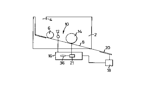
Referring to Fig. 1, a validator 2 has an entry
4 through which coins, such as that shown at 6, may be
inserted. The coins fall on to a ramp 8 and then roll
- down the ramp through a sensing area generally
indicated at 10. The sensor area 10 contains one or
more sensors for measuring the characteristics of the
coin in order to determine its validity and
-
CA 02244102 1998-07-23
WO 97/29460 PCT/GB97/00229
denomination.
The illustrated embo~;m~nt includes a relatively
small sensor 12 in the form of a coil positioned along
side the ramp so that the face of the coin 6 passes in
proximity to the coil 12 a9 the coin rolls down the
ramp. The coil 12 may be double-sided, i.e. there may
be a separate coil on each side of the ramp so that
the coin passes therebetween. This sensor could for
example be used for thickness sensing.,
lQ A further sensor 14 comprises a double-sided
coil, i.e. separate coils 14' and 14'l (see Fig. 2)
positioned one on each side of the ramp 8 so that the
coin 6 passes between the coils.
The validator 2 is a multi-denomination
validator, i.e. it is used for determining the
validity and denomination o~ a number of different-
denomination coins. The coils of the sensor 14 are
~arger than the largest-sized coin amongst the
denominations to be validated by the validator 2. The
lowermost parts of the coils of the sensor 14 are
close to the ramp 8. These features mean that the
proportion of the overlapping areas of the coils 14'
- and 14ll which is occupied by the coin varies to the
greatest extent with different denominations. This
impro~es the discrimination between coins of similar,
but slightly different, diameters.
, .
CA 02244102 1998-07-23
W O 97/29460 PCT/GB97/00229
The sensors 12 and 14 are coupled to a validation
circuit 16, which drives the sensors, processes the
signals from the sensors and determlnes validity and
denomination. The circuit 16 can then generate
suitable output signals, ~or example a signal which
dri~es a solenoid 18 to control the operation of an
accept/reject gate 20 located at the end o~ the ramp
8, thereby determi n; ng the final destination o~ the
coin 6.
The diameter measuring part 21 of the validation
circuit is shown in Fig. 2. Thls comprises an
oscillator ~ormed by an inverter 22 ~in the
illustrated em~odiment this is formed ~y three
individual series-connected integrated circuit
inverter gates). There is a feedback path from the
output 24 o~ the inverter 22 to its input 26. This
feedback path includes a series circuit comprising a
resistor 2~ and the two coils 14' and 14". A
capacitor 30 is connected ~etween the junction o~ the
2~ resistor 28 and the coil 14', on the one hand, and
ground 32 on the other hand. A capacitor 34 is
connected in parallel between the input 26 and ground
32.
The circuit thus ~orms a simple oscillator, with
the frequency at the output 24 being determined by the
values of the capacitors 30 and 34 and the inductive
CA 02244102 1998-07-23
W O 97J29460 PCT/GB97/00229
values o~ the coils 14' and 14", in addition to the
mutual inductance between the coils 14' and 14". The
value o~ this mutual inductance changes as a coin 6
passes between the coils 14' and 14", to a degree
which depends upon the amount by which the overlapping
area between the coils 14' and 14" is occluded by the
coin 6. The output 24 o~ the oscillator 22 is, as
schematically illustrated in Fig. 1, delivered to a
counter 36. The counter 36 can count the oscillations
of the oscillator 21 and thereby determine its
~requency.
The oscillator 21 includes two switches, 38 and
40 which, in the configuration shown in Fig. 2,
inte-connect the coils 14' and 14" in an opposed
con~iguration, i.e. so that they are driven in
opposite senses. By simultaneous operation of the
switches 38 and 40, the connections to the coil 14"
are reversed, so that the coils are coupled in a
series-aiding manner, i.e. they are driven in the same
sense.
Assuming that the inductances o~ the coils 14'
and 1a~ are Ll and L2, respectively, and that the
- mutual inductance therebetween is M, then when the
coils are connected in a series-aiding con~iguration,
the total inductance LA is:
LA--Ll + L2 ~ 2M
CA 02244102 1998-07-23
W 097/29460 PCT/GB97/00229
When connected in the opposing con~iguration, the
total inductance ~O is:
LO = L1 + L2 - 2M
The period Pa of the oscillator 21, in the aiding
configuration, is given by:
PaZ = 4~2C~L1+L2+2M)
where: 1 1 + 1
c cl c2
In the opposing configuration, the period Po is given
~y:
po2 = 47r2C (I~l+L2-2M)
Therefore, the di~ference between the periods in
the two configurations is given ~y:
pa2 _ po2 = 4~C~4M), i.e.:
~Pa+Po)~Pa-Po~ = 4~2C~4M)
But Ll + L2 ~ 2M, and therefore the change in (Pa
+ Po) ~or di~ferent values of mutual inductance is
proportionately much smaller than that in ~Pa - Pa).
Therefore, k(Pa-Po) = 4~2C~4M)
There~ore, the dif~erence in the period
measurement is substantially proportional to the
mutual coupling, M, between the coils.
The circuit operates as ~ollows. The switches 38
and 40 are operated simultaneously at intervals which
are significantly shorter than the time taken ~or the
CA 02244102 1998-07-23
WO 97/29460 PCT/GB97/00229
coin to pass between the coils 14' and 14". The
interval may for example be approximately 0.5 ms.
Each time the coils are switched to the aiding
con~iguration, there is a brief delay, of for example
5 oscillator cycles, to allow the oscillator to
settle, and then the counter 36 is caused to start
counting up from zero. Each time the coils are
switched to the opposing configuration, there is
another brief delay before the counter 36 is caused to
start counting down. At the end of the interval, the
count reached by the counter 36 will be representative
o~ the mutual inductance M, and this value is
transferred to a register.
The idle value of M, Mi, is measured in this
1~ manner when no coin is present between the coils 14'
and 14". The idle value could be measured be~ore a
coin is inserted, after a coin is inserted and be~ore
it reaches the coils, or after the coin leaves the
coils ~which is the preferred arrangement). A~ter the
coin starts to enter the space between the coils, the
value M is repeatedly measured. The mutual inductance
M will decrease as the coin occludes more of the area
between the coils. The minimum value Mm obtained
during the passage o~ the coin through the coils is
2~ determined (this corresponding to the position in
which the coin is fully within the overlapping area of
CA 02244102 1998-07-23
W O 97/29460 PCTIGB97/aO229
11
the coils 14' and 14"). A diameter measurement D is
then obtained as follows:
D = Mi - Mm
This then can be compared with stored values to
determine whether the measurement is indicative of a
particular type of coin denomination.
It would be possible to base the diameter
measurement simply on Mm, but by taking into account
the idle value Mi it is possible to avoid the ef~ects
of variations in the mutual inductance due to changes
in the coil positions, e.g. as a result of temperature
changes, etc.
In the preferred embodiment, the frequency of the
oscillator 21 exceeds 10 kHz, and there is time for at
least 15 measurements when the smallest-sized coin
passes between the coils.
This technique allows the diameter to be measured
while avoiding ~noise" effects due to embossing, and
avoiding or substantially mitigating the effects of
"lift-off".
If desired, the switching of the coil
con~iguration could be arranged to be started by the
- detection of arrival of a coin to be tested.
~ In the above embodiment, the coils are connected
in series, in either aiding or opposing configuration.
It wol.ld alternatively be possible to switch between
CA 02244l02 l998-07-23
W O 97/29460 PCT/GB97/00229 12
aiding and opposing parallel con~igurations, which
produces a similar result.