Note: Descriptions are shown in the official language in which they were submitted.
CA 02244137 1998-07-23
GR 96 P 1070 New Version
i '~'F~~~SLATION
Description
Control device, in particular for a motor vehicle
The invention relates to a control device in
accordance with the preamble of patent claim 1.
Such a control device a.s known from the publica-
tion DE 42 40 754 A1. A double T-shaped cooling plate
forms two outer walls of the housing and a plug component
forms a further wall. The cooling plate and the plug
component are held together by two covers.
The publication DE 41 02 265 A1 discloses a
control device whose housing is formed by a cooling plate
and an upper housing component. In the interior of the
housing, a printed circuit board fitted with an
electrical circuit is arranged on the upper side of the
cooling plate. A plug component with plug pins a.s
attached to the underside of the cooling plate. The plug
pins project through an opening in the cooling plate and
lead into the printed circuit board which extends over
the opening, so that the plug pins and circuit are
electrically conductively connected.
This control device permits only a restricted
number of plug pins, since the region of the printed
circuit board which is provided for receiving the plug
pins and is arranged over the opening of the cooling
plate cannot be used for the actual electrical circuit.
For this reason, a large number of plug pins makes it
necessary for the printed circuit board to have a large
surface area and thus a control device with large dimen-
sions, which is disadvantageous when installation is in
a motor vehicle with its restricted space available. Even
though advances a.n technology have made it possible to
have a smaller printed circuit board with an unchanged
quantity of circuitry and the same number of plug pins,
the dimensions of the control device are, however,
reduced only to a small degree since a relatively large
region of the printed circuit board has to be made
CA 02244137 2001-02-27
20365-3898
2
available to received the plug pins, and this region cannot be
made smaller. In addition, the position of the plug component
with respect to the printed circuit board is fixed.
The known control device concept is also dis-
advantageous with respect to the point of view of
electromagnetic compatibility, since electromagnetic radiation
is emitted directly onto the printed circuit board via the plug
pins and through the opening in the cooling plate. Signal paths
which emit weak radiation and those which emit strong radiation
can only be spatially separated from one another on the printed
circuit board. In addition the plug pins lead into the central
region of the printed circuit board, which results in omni-
directional emission of electromagnetic waves onto the entire
circuit.
The object of the invention is to provide a control
device which has compact dimensions, and which can hold one or
more plug components, even with a large number of plug pins,
and at the same time the surface area of the printed circuit
board fitted with the circuit is small.
The invention provides a control device for a motor
vehicle, comprising: a cooling plate; a first printed circuit
board on an upper side of the cooling plate; a plug component
with plug pins, said plug component being arranged on a side of
the cooling plate facing away from the first printed circuit
board; a second printed circuit board arranged between the plug
component and the cooling plate, on the side of the cooling
plate facing away from the first printed circuit board, the
plug pins of the plug component being in contact solely with
the second printed circuit board; and the second printed
circuit board being electrically conductively connected to the
first printed circuit board via connecting elements.
CA 02244137 2001-02-27
20365-3898
2a
The broad side of the cooling plate on which the
first printed circuit board is arranged is referred to below as
"upper side". The other broad side of the cooling plate is
referred to below as "underside". The spatial specifications
"above" and "below" the cooling plate are used in a
corresponding fashion.
The solution according to the invention has the
advantage that the control device can have, with respect to the
underside of its cooling plate, one or more plug components,
even with a large number of plug pins.
CA 02244137 1998-07-23
' ' GR 96 P 1070 - 3 -
' _ The size of the cooling plate then depends on the size of
the first printed circuit board and thus on the quantity
of electric circuitry or on the surface area necessary
for the plug components, without these two influencing
parameters having to be correlated.
Preferably, the plug component is arranged on a
lower housing component which receives the second printed
circuit board and which is mechanically connected to the
cooling plate or to the upper housing component. The plug
pins lead into the second printed circuit board and are
electrically conductively connected to the first printed
circuit board via the connecting elements. Further
advantages of the control device according to the inven-
tion are disclosed in the description of the figures.
Advantageous developments of the invention are
defined a.n the subclaims.
The invention and its developments are explained
with reference to the drawings, in which:
Figure 1 shows a longitudinal section through a control
device according to the invention,
Figure 2 shows a lower housing component in a
perspective view from below,
Figure 3 shows a cut-away longitudinal section through
a control device,
Figure 4 shows a further cut-away longitudinal section
through a control device,
Figure 5 shows a perspective view from above of a
control device which a.s cut away in various
planes,
Figure 6 shows an exploded view of a control device,
Figure 7 shows an exploded view of components of a
control device,
Figure 8 shows a further longitudinal section through a
control device, and
i
CA 02244137 1998-07-23
GR 96 P 1070 - 4 -
_ Figure 9 shows a cross section through a further control
device according to the invention.
Identical elements a.n the figures have the same
references in all the figures.
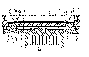
Figure 1 shows a control device according to the
invention in a longitudinal section with an upper housing
component 1, a lower housing component 2 and a cooling
plate 3 between upper housing component 1 and lower
housing component 2. Arranged underneath the cooling
plate is a plug component 6 with plug pins 61. Mounted on
the cooling plate 3 is a first printed circuit board 4
which is fitted with an electrical circuit with
components 41. A second printed circuit board 5 is
mounted on the inside 21 of the lower housing component
2, facing the cooling plate 3 and over the plug component
6. Two connector components 7 are integrally connected to
the second printed circuit board 5 and contain regions 72
with contact areas 83. The contact areas 83 are connected
via bonding wires 82 to the first printed circuit board
4. The lower housing component 2 contains webs 22 with
ramps 221 and end sides 222, the regions 72 of the
connector with the contact areas being arranged on the
end sides 222 of the webs 22. The webs 22 project through
openings 31 in the cooling plate 3.
The cooling plate 3 is implemented as a metal
plate, for example made of aluminum, sheet metal or as a
diecast component or punched component made of metal, and
serves to cool the electrical components 41 on the
printed circuit board 4, in particular also to cool power
components (not shown in Figure 1) which are arranged on
the printed circuit board 4, but even more satisfactorily
directly on the cooling plate 3 or on the cooling plate
3 via heat-conducting component holders. Secondly, the
cooling plate 3 protects the electrical circuit on the
printed circuit board 4 against electromagnetic radiation
(EMC radiation) . Here, the cooling plate 3 forms, with
the upper housing component 1 composed of metal, a
virtually enclosed, EMC-shielding housing chamber l, 3
made of metal. The upper housing component 1 and cooling
<IMG>
CA 02244137 1998-07-23
GR 96 P 1070 - 5 -
_ are connected mechanically to one another here using a
conventional connecting technique such as crimping,
beading, bonding, bolting.
The first printed circuit board 4 can be bonded
or laminated onto the cooling plate 3 as a conventional
single-layer or multilayer printed circuit board or as a
flexible printed circuit board with a bonding agent which
is an electrical insulator but a good thermal conductor.
The first printed circuit board 4 can also be fitted with
a hybrid circuit.
The lower housing component 2 is preferably
manufactured (encapsulated by injection molding) in one
piece with the plug component 6 from plastic . The webs 22
are also implemented here so as to be integral with the
lower housing component 2. The plug pins 61 are
encapsulated by injection molding, or inserted in the
same manufacturing step. The lower housing component 2 is
connected using a known connecting technique, for example
with a combined clip-on and bonded connection (see
latching hook 23 and sealing compound 24 in Figure 8), to
the cooling plate 3. The cooling plate 3 has, for this
purpose, appropriate contours on its circumference. Lower
housing component 2, upper housing component 1 and metal
plate are connected to form a watertight housing.
The second printed circuit board 5 is bonded onto
the inside 21 of the lower housing component 2. It is
implemented in one piece together with the connector
components 7 as a flexible printed circuit board and is
attached by its ends to the end sides 222 of the webs 22.
The plug pins 61 lead into the flexible printed circuit
board 5, 7 and are soldered to the flexible printed
circuit board 5, 7 on its upper side. As is clear from
Figure 5, the flexible printed circuit board 5, 7 has
conductor tracks 81 which lead from the plug pins 61 to
the contact areas 83. The contact areas 83 are arranged,
using the webs 22, level with the first printed circuit
board 4 and are connected thereto by means of bonding
wires. In this way, the plug pins 61 are electrically
conductively connected to the first printed circuit board 4
CA 02244137 1998-07-23
- - GR 96 P 1070 - 6 -
by means of the conductor tracks 81, the contact areas 83
and the bonding wires 82 as connecting elements 8.
Figure 3 shows a cut-away longitudinal section of
the control device according to the invention, which
differs from Figure 1 essentially in the fact that the
flexible printed circuit board 5, 7 leads via bevelled
ramps 221 of the webs 22 to their end sides 222.
Figure 4 shows a further variant of the
connection between the second and first printed circuit
boards 5 and 4: The flexible printed circuit board 5, 7
leads along the ramps 221 through the openings 31 of the
cooling plate 3 and is then not attached by its ends to
the end sides 222 of the webs 22 but rather folded over
onto the first printed circuit board 4 so that at least
the region 72 with the contact areas 83 bears on the
first printed circuit board 4. The contact areas 83 are
electrically conductively connected to corresponding
contact points of the first printed circuit board 4 by
soldering or with conductive adhesive, so that, again, an
electrically conductive connection is produced from the
plug pins 61 via the conductor tracks 81 and the contact
areas 83 to the first printed circuit board 4.
Figure 7 shows, in an exploded view, a further
variant of the connection between the second and first
printed circuit boards 5 and 4 to those elements of the
control device which are arranged facing the underside of
the cooling plate 3: The second printed circuit board 5
a.s implemented as a rigid printed circuit board. Instead
of the rigid printed circuit board, a flexible printed
circuit board may also be provided. Conductor tracks (not
shown) of the second printed circuit board 5 electrically
connect the plug pins 61, leading into the second printed
circuit board 5 in the assembled state, to module
locations 52. Connector components 7 which are
implemented as multipoint connectors 71 are plugged into
these module slots 52 and soldered to the conductor
tracks of the second printed circuit board 5. The
multipoint connectors 71 contain contact pins 84 which
are encapsulated by injection molding and which are, if
CA 02244137 1998-07-23
GR 96 P 1070 - 6a -
' _ _ appropriate, implemented as punched/bent components. On
the
CA 02244137 1998-07-23
GR 96 P 1070 - 7 -
end side of the multipoint connectors, contact areas 83
are arranged. When the control device a.s assembled, the
multipoint connectors project through the opening 31 in
the cooling plate 3, the contact areas 83 in this
embodiment, too, being arranged on the same plane as the
first printed circuit board 4 so that the contact areas
83 can be bonded to the first printed circuit board 4 a.n
one plane.
Figure 8 shows a longitudinal section of such a
control device with multipoint connectors 71 as connector
components 7.
The multipoint connector can also be implemented
in a t shape so that the multipoint connector is fitted,
with the underside of the longitudinal bar, into the
module location of the second printed circuit board. The
contact areas are then provided on the underside of the
transverse bar. When such a multipoint connector is
fitted on, the contact areas are fitted from above onto
corresponding contact points of the first printed circuit
board and electrically connected thereto (in accordance
with Figure 4).
The mechanical connection between second printed
circuit board 5 and lower housing component 2 may be of
any desired configuration, for example by means of
rivets, domes, bonding agents or screws.
In the case of a plug component with large
dimensions, the second printed circuit board may, under
certain circumstances, be arranged with its entire extent
over the plug component, so that, in this embodiment,
lower housing component and plug component form one unit.
Here too, the lower housing component forms, together
with the cooling plate, a housing chamber for receiving
the second printed circuit board.
Figure 2 shows, in a perspective view from below,
a lower housing component 2 which has two plug components
6.
Figure 6 shows an exploded view of the control
device according to Figure 1, which has two openings 31
in the edge region
CA 02244137 1998-07-23
GR 96 P 1070 - 8 -
- - of the cooling plate 3. It is advantageous to make these
openings 31 in the edge region of the cooling plate 3
owing to the EMC radiation which is conveyed via the
connecting elements 8 into the housing chamber 1, 3.
Depending on the number of plug pins 61, the cooling
plate 3 can have one, two, three or four openings, in
which case, in an embodiment With four openings 31, the
first printed circuit board 4 is preferably surrounded by
these four openings 31.
Figure 9 shows a longitudinal section through a
further control device according to the invention with an
upper housing component l, a lower housing component 2,
and a cooling plate 3 between upper housing component 1
and lower housing component 2. Arranged underneath the
cooling plate 3 is a plug component 6 with plug pins 61
shown by dashed lines. A first printed circuit board 4
which is fitted with an electrical circuit with
components 41 is mechanically connected to the upper side
32 of the cooling plate 3 in a permanent fashion. A
second printed circuit board 5 is mounted on the under-
side 33 of the cooling plate 3 between cooling plate 3
and plug component 6. First printed circuit board 4 and
second printed circuit board 5 are electrically connected
to one another via connecting elements 8 which are
implemented as bonding wires.
The first printed circuit board 4 can be bonded
or laminated onto the cooling plate 3 as a conventional
single-layer or multilayer printed circuit board or as a
flexible printed circuit board with an adhesive layer
which is an electrical insulator but a good thermal
conductor. The first printed circuit board 4 is also to
be understood here generally as a circuit carrier which
is fatted, in particular, with a circuit for controlling
the engine or gearbox of a motor vehicle. This circuit
carrier is preferably implemented as a hybrid circuit
carrier, and therefore has a ceramic base.
The second printed circuit board 5 as implemented
in Figure 9 preferably as a rigid, conventional plastic
printed circuit board which is bonded or laminated onto
CA 02244137 1998-07-23
GR 96 P 1070 - ga -
the cooling plate 3. Here, it is not necessary for the
entire surface of the printed circuit board
CA 02244137 1998-07-23
GR 96 P 1070 - 9 -
- ~ to be in contact with the cooling body. As a result of
the second printed circuit board being mounted on or
permanently connected to the cooling body, forces which
are induced in the plug component 6, and which are caused
for example by a cable harness in the motor vehicle which
is connected to the plug component and is oscillating
with it, are not transmitted to the electrical connecting
elements 8. For this purpose, the plug component 6 is
preferably riot mechanically connected to the second
printed circuit board, with the exception of the electri-
cal contact points. Owing to the permanent mechanical
connection between the second printed circuit board 5 and
the cooling plate 3 , forces Which are possibly induced on
the second printed circuit board 5 via the electrical
contact points are not transmitted to the connecting
elements 8, which are sensitive to mechanical stressing
and are at risk of fracturing, between the first and
second printed circuit boards 4 and 5. This makes the
control device more reliable.
The plug pins 61 are fitted and/or pressed into
the second printed circuit board 5 and, if appropriate,
soldered thereto on its upper side 52. In order to
receive the tips of the plug pins projecting out of the
upper side of the second printed circuit board 5, the
cooling plate 3 has a recess 34. In contrast with the
first printed circuit board 4, the second printed circuit
board 5 covers openings 31 in the cooling plate 3. The
second printed circuit board 5 has conductor tracks which
are not shown and which lead from the plug pins 61 to
contact areas 51 which are arranged in the region of the
openings 31 on the upper side 52 of the second printed
circuit board 5.
If the plug pins 61 on the upper side 52 of the
second printed circuit board 5 are soldered thereto and
if, for example, the second printed circuit board 5 is
implemented as a single-layer printed circuit board with
conductor tracks on its upper side 52, the second printed
circuit board 5 has an insulating layer on its upper side
52, at least in the region in which said printed circuit
CA 02244137 1998-07-23
GR 96 P 1070 - 9a -
' ~ ' board 5 is attached by its upper side 52 to the underside
33 of the cooling plate 3. Alternatively, the second
printed circuit board 5 is implemented as a multilayer
printed circuit board. It is also particularly
advantageous to
CA 02244137 1998-07-23
GR 96 P 1070 - 10 -
' implement the plug component 6 as an SIB (surface mounted
device) plug component. In this way, the plug pins 61 on
the underside 53 of the second printed circuit board 5
are soldered or bonded thereto. The second printed
circuit board 5 then preferably has conductor tracks on
its underside 53. From the contact areas 51 on the upper
side 52 of the second printed circuit board 5 there is
then through-contacting to the conductor tracks on the
underside 53.
At least some of the plug pins 61 are electri-
cally conductively connected directly to the contact
areas 43 of the first printed circuit board 4 via the
conductor tracks of the second printed circuit board 5,
the contact areas 53 of the second printed circuit board
5 and the connecting elements 8. However, electrical
components may also be arranged on the second printed
circuit board 5, the signals fed via the plug pins 61
being essentially pre-processed by means of these
components and only then being fed to the circuit on the
first printed circuit board 4.
The connecting elements 8 are implemented, in
particular, as bonding wires between the contact areas 51
on the second printed circuit board 5 and contact areas
43 on the upper side 42 of the first printed circuit
board 4. In particular in the case of a hybrid circuit
carrier as first printed circuit board 4, bonding wires
are advantageous as connecting elements 8.
However, other connecting elements 8 may also be
used, for example multipoint connectors in accordance
with Figure 7.
The plug component 6 is connected to the cooling
plate 3 with rivets, screws or by caulking or bonding.
The attachment means here can be fitted through recesses
in the second printed circuit board 5 or be arranged next
to the second printed circuit board 5. According to the
invention, the plug component 6 is mounted a.n a region B
on the cooling plate 3, which region is characterized by
the electrical contact points between the plug
CA 02244137 1998-07-23
GR 96 P 1070 - 11 -
- - ~ pins 61 and the second printed circuit board 5, as a
result of which the connection between plug component 6
and cooling plate 3 is implemented in a rattle-free
fashion. As a result of this mechanical attachment,
forces which are induced a.n the plug component 6, and
which are caused for example by a cable harness in the
motor vehicle which is connected to the plug component 6
and which a.s oscillating with it, are absorbed directly
at their point of induction, i.e. the plug component 6,
without being able to propagate over further components
of the control device which are capable of oscillating.
In order to avoid loading the contact points between the
plug pins 61 and the second printed circuit board 5, the
points, i.e. the attachment points, at which forces are
transmitted from the plug component 6 to the cooling
plate 3 and are absorbed, are arranged near to the
contact points. These forces are not passed on to the
second printed circuit board 5 and the connecting
elements 8. In particular the thin-wired bonded
connections, at risk of fracturing, between the first and
second printed circuit boards 4 and 5 are relieved of
mechanical stress even in the event of strong vibrations
of the plug component 6. The entire control device is of
mechanically rigid design in terms of possible vibration
loading and, for this reason, is reliable during
operation in a rough environment such as in a motor
vehicle, for example.
The lower housing component 2 forms, together
with the cooling plate 3, a sort of chamber a.n which the
second printed circuit board 5 is arranged with the plug
component 6. If the lower housing component 2 is made of
metal, good electromagnetic shielding is obtained, since
the entire housing composed of cooling plate 3, upper
housing component 1 aad lower housing component 2 is
manufactured from metal, so that the electrical circuit
and the conductor tracks in the interior of the housing
are well shielded.
When the control device is used, for example, in
the engine compartment, the control device has to have a
CA 02244137 1998-07-23
GR 96 P 1070 - lla -
- . ~ particularly sealed design: The cooling plate 3 has, for
this purpose, on its upper side and underside 32 and 33
grooves 321 and 331 which are filled with a sealing mass
8. The edges of the upper housing component 1 and lower
housing component 2 are
CA 02244137 1998-07-23
GR 96 P 1070 - 12 -
- _ . respectively introduced into the appropriate groove.
Lower housing component 2 and plug component 6 are sealed
with respect to one another, too. The plug component 6
has, in accordance with the figure, a groove 62 which is
filled with a sealing mass 8 and in which the
corresponding edge of the lower housing component 2
engages.
Preferably, the plug component 6 a.s manufactured
in one piece with the lower housing component 2 from
plastic which is possibly shot through with metal parti-
cles a.n order to improve the electromagnetic shielding.
In all cases, the actual plug component 6 also has to be
connected permanently to the cooling plate 3, in particu-
lar near to the contact points between the plug pins 61
and the second printed circuit board 5.
The control device concept according to the
invention has, in particular, the following advantages:
Plug components can be arranged over the entire surface
area of the cooling plate facing its underside, or a plug
component with a large number of plug pins can take up
the entire surface area of the cooling plate for itself
without the first printed circuit board having to be
enlarged owing to the number of plug components/plug
pins.
The plug component can be arranged at any desired
point on the underside of the cooling plate.
The control device can have a large number of
plug pins, since the plug pins are firstly connected to
the conductor tracks of the second printed circuit board:
As a result of the relatively small structural size of
conductor tracks, contact pins, contact areas and bonding
wires as connecting elements between the second printed
circuit board and the first printed circuit board, the
coarse spacing pattern of the plug pins which are of
thick design owing to their mechanical loading is
converted into a significantly finer connecting pattern
of the contact areas. Since the aforementioned connecting
elements between plug pins and first printed circuit
board are hardly subject to mechanical loading, they can
CA 02244137 1998-07-23
GR 96 P 1070 - 13 -
- . - be of thin design.
The placing of the connector component is inde-
pendent of the placing of the plug component: In particu-
lar in terms of the electromagnetic shielding, the
connector component is therefore preferably arranged at
the edge of the electrical circuit/first printed circuit
board, whereas the plug component is arranged in a stable
way in the central region underneath the cooling plate.
On the other hand, when another plug component is used,
for example with another signal assignment of the plug
pins or a larger/smaller number of plug pins, or when an
arrangement of an additional plug is used, all that is
necessary is to change the routing of the conductor
tracks on the second printed circuit board and to change
the lower housing component/plug component: The actual
electrical circuit can remain unchanged.
The free selection of the conductor track routing
on the second printed circuit board permits electromag-
netically compatible conductor track routing: in this
Way, sensitive signal paths can already be separated on
the second printed circuit board from signal paths with
strong radiation, an earthline possibly being arranged
between these signal paths in order to absorb EMC
radiation. EMC-sensitive conductor tracks are fed, for
example in a spatial grouping, via a first connector
component to the first printed circuit board: Components
which are susceptible to interference are then arranged
near to the first connector component on the first
printed circuit board. Conductor tracks which emit strong
radiation are however fed, in a spatial grouping, via a
second connector component to the first printed circuit
board: Components which are not susceptible to
interference are then arranged near to the second
connector component on the first printed circuit board.
By means of the cooling plate and the upper
housing component, a virtually electromagnetically sealed
housing chamber is provided in which the first printed
circuit board with the electrical circuit is arranged. In
order to improve the EMC properties of the control device
<IMG>
CA 02244137 1998-07-23
GR 96 P 1070 - 14 -
the electromagnetic radiation which enters the control
device via the plug pins can already be diverted near to
the plug component by means of a metallized region on the
second printed circuit board. If the second printed
circuit board is implemented as a multilayer printed
circuit board, one of the layers can contain the
metallized region.
Electr3.ca1 components can also be arranged on the
second printed circuit board.
A bonded connection between contact areas on the
connector component and the first printed circuit board
is advantageous in particular if the electrical circuit
is implemented as a hybrid circuit. If the contact areas
on the connector component and appropriate contact points
on the first printed circuit board, which are connected
via bonding wires, are in one plane (see Figure 3), the
tensile strength of the bonded connection a.s increased,
since vertical stressing of the bonded connection does
not immediately cause the bonding wires to tear, nor does
horizontal stressing. Therefore, the bonding wires may be
of thinner design; in addition, they are significantly
shorter than in the case of a bonded connection between
contact areas on different levels. Overall, the bonded
connection is therefore more reliable.
In the control device according to the invention,
sufficient space is also provided to produce the bonded
connections: according to Figure 3, sufficient space is
provided on the left-hand side of the contact areas 83 so
that a bonding tool can attach the bonding wire to the
contact area 83. The left-hand part of the contact area
is not blocked by plugs or other housing components. On
the right-hand side of the contact points arranged on the
first printed circuit board, sufficient space is also
provided so that the bonding tool can tear off protruding
bonding wires towards the right-hand side of the contact
points. Here too, the right-hand part of the contact
points
CA 02244137 1998-07-23
GR 96 P 1070 - 15 -
' ' ~ is not adversely affected by a plug or other housing
components.