Note: Descriptions are shown in the official language in which they were submitted.
CA 02244301 2002-02-11
1
WIRE TERMINAL BLOCK FOR COMMUNICATION CONNECTORS
Field of the Invention
The present invention relates to connectors for
communication wires and cables, and particularly to a
spring wire terminal block for use in communication jacks.
Discussion of the Known Art
A compact communications jack connector is disclosed
in U.S. Patent No. 5,096,442 (Mar. 17, 1992). The known
connector is formed from a unitary lead frame in which
eight flat, elongated conductive elements connect spring
jackwire terminals at one end of the frame with
corresponding wire connection terminals at the other end
of the frame. The wire connection terminals are insulation
displacement connectors (IDCs) of the "slotted-beam" type.
For example, see U.S. Patents 3,027,536 (Mar. 27, 1962);
3,798,587 (Mar. 19, 1974) and 4,826,449 (May 2, 1989).
In the mentioned '442 patent, the lead frame is
placed against a bottom surface of a dielectric spring
block, the jackwire terminals are wrapped around a
tongue-like protrusion on the block, and the elongated
conductive elements are positioned flat and parallel to
one another on the block bottom surface. Individual IDC
terminals of the lead frame are folded onto side surfaces
of the block. Slots in the IDC terminals align with
corresponding wire-receiving slots formed in the block,
and a cover is placed around the block including the
wrapped IDC terminals. The tongue-like protrusion of the
block is received in a jack frame, and the jackwire
terminals are aligned so that when a connecting plug is
inserted the jack frame, the jackwire terminals connect
electrically with corresponding wire leads in the plug.
A communication jack made by AMP Corporation (Part
No. 557901-1) and intended for high data rate applications
CA 02244301 2002-02-11
2
includes a printed wire board, jackwires that emerge from
a top surface of the board and bend sharply back over the
board, and sets of wire connection terminals at the sides
of the board. Two separate terminal covers are each held
in place by pins which pass horizontally through openings
in the terminal bases. The top surface of the wire board
is left exposed between the separated terminal covers. A
front end of the board slides into a jack frame, and tabs
on the sides of the board snap in slots in rear side walls
of the jack housing. The jack housing also has a rear
bottom wall that extends over the bottom surface of the
wire board.
A device for reducing crosstalk exhibited by certain
connections is known in the prior art. The device
comprises a printed wire board having several dielectric
layers. Pairs of conductor paths are formed on selected
layers, and a conductor path of one pair is vertically
aligned and spaced from a conductor path of another pair
on an adjacent layer. A given set of vertically aligned
paths acts electrically as a capacitor plate that
cooperates with a horizontally adjacent set of vertically
aligned paths, to compensate for or reduce crosstalk
exhibited by a given connector. As far as is known, this
crosstalk reduction scheme has not been applied in a
communication jack.
U.S. Patent 5,186,647 (Feb. 16, 1993) shows a high
frequency electrical connector similar to the mentioned
U.S. Patent 5,096,442; but wherein certain pairs of the
parallel conductive elements cross over one another as a
means for reducing crosstalk. Other arrangements for
reducing crosstalk are disclosed by U.S. Patents 5,432,484
(Jul. 11, 1995); 5,299,956 (Apr. 5, 1994); and 5,580,270
(Dec. 3, 1996) .
It is also known to construct a terminal post with a
retaining portion formed of two arcuate spring members
CA 02244301 2002-02-11
3
which are separated by an opening, thus resembling a
"needle eye". See, for example, U.S. Patent No. 4,206,964
(Jun. 10, 1980). See also U.S. Patent Des. 345,268
(Jan. 10, 1995) showing a telecommunications terminal clip
having a slotted retaining portion.
There remains a need for a durable high frequency
communication jack that will minimize or compensate for
crosstalk between two or more signal paths through the
jack, particularly when a communication plug, which alone
may tend to introduce undesirable crosstalk, is mated with
the jack. The resulting plug-jack connection should
nonetheless allow for high data rate transmission in a
wired network, whether local or global.
The desired jack should also be easy to manufacture
in high volume, and be compliant. That is, the jack should
maintain its high performance characteristics
notwithstanding repeated connection with and disconnection
from mating plugs, and use with plugs having different
numbers of wire conductors. In particular, unused jackwire
terminals should not be permanently deformed when
deflected by plug bodies that carry fewer wire conductors
than the number of jackwire terminals in the jack. With
respect to manufacturing steps, a communication jack that
uses minimal horizontal or side-wise tool movements during
assembly, and relies primarily on vertical or straight
up-and-down tool motion for its construction, is also
desirable.
Summary of the Invention
According to the invention, a wire terminal block for
communication connectors includes a mandrel, and a frame
including a pair of legs extending from opposite ends of
the mandrel. The legs are constructed and arranged to be
mounted on a printed wire board and to support the mandrel
against an edge of the board near a number of terminal
CA 02244301 2002-02-11
4
wires that emerge from the board to contact a mating
connector. A number of slots are formed along the mandrel,
and an inner contour at a base of each slot is configured
to form a desired bend radius in the terminal wires when
the wires are seated in corresponding ones of the slots
and are wrapped about the mandrel within the slots.
According to another aspect of the invention, a wire
terminal block for communication connectors includes a
mandrel, and a frame constructed and arranged to be
mounted on a printed wire board and to support the mandrel
on the board near a number of terminal wires that emerge
from the board to contact a mating connector. A number of
slots are formed along the mandrel, and an inner contour
at a base of each slot is configured to form a first bend
radius in the terminal wires at a side of the wire board
from which the terminal wires emerge, and to form a second
bend radius in the terminal wires with which the wires
angle back over an opposite side of the board to contact
the mating connector, when the terminal wires are seated
in corresponding ones of the slots and are wrapped about
the mandrel within the slots.
For a better understanding of the invention,
reference is made to the following description taken in
conjunction with the accompanying drawings, and the scope
of the invention will be pointed out by the appended
claims.
CA 02244301 1998-07-29
Brief Descr,~,ptl.On_ of the Drawing
In the drawing:
FIG. 1 is an exploded view of a high frequency
communication jack assembly and a mating jack frame,
5 according to the invention;
FIG. 2 is an enlarged perspective view of a spring
jackwire block in the jack of FIG. 1;
FIG. 3 is a side view, partly in section, of the
jackwire block in FIG. 2 as taken along line 3-3 in FIG.
2;
FIG. 4 is a plan view of the jackwire block as seen
from the bottom in FIG. 2;
FIG. 5 is an enlarged side view of a terminal housing
of the jack as seen from the rear left side in FIG. 1;
FIG. 6 is a bottom plan view of the housing in FIG.
5; and
FIG. 7 is an enlarged side elevation view of a
connector terminal in the jack of FIG. 1 with the terminal
housing in place.
Detailed Dee~rri~~ion of the Invention
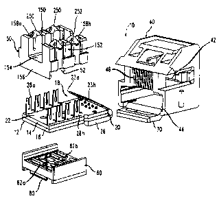
FIG. 1 is an exploded view of a high frequency
communication jack 10 according to the invention. The
jack 10 includes a printed wire board 12 which preferably
is multi-layered. Although two layers 14, 16 are shown in
FIG. 1, the wire board 12 may comprise one layer with
printed conductive paths on one or both sides, or
additional layers with conductive paths on each layer,
depending on the desired crosstalk reduction scheme. In
FIG. 1, wire board 12 has conductive paths (see FIG. 7) on
the layers 14, 16 which paths extend between a jackwire
terminal region 18 near a front edge 20 of the board 12,
and a wire connection terminal region 22 at a rear portion
of the board.
A number, for example, eight spring jackwires 23a to
23h extend from the front of the board 12 through the
CA 02244301 1998-07-29
6
jackwire terminal region 18, at an acute angle relative to
the top surface of the wire board 12 to connect with a
communication plug (not shown) when the plug is placed in
the jackwire terminal region 18. The jackwires 23a-23h
connect at their bottom ends to corresponding conductive
paths of the wire board 12, so that the conductive paths
form a part of one or more communication signal paths when
the communication plug is connected with the jackwires.
Typically, each communication signal path will be
comprised of a different pair of conductive paths on the
wire board 12. In the disclosed embodiment, up to four
communication signal paths can be supported by the eight
jackwires 23a-23h, with a corresponding number of
conductive paths on the board.
Preferably, the conductive paths associated with the
wire board 12 are configured individually or in
combination with other discrete components (not shown)
such as resistors, capacitors and inductors, to compensate
for or to reduce crosstalk otherwise developed in a
communication signal path when the plug is connected with
the jackwires.
The bottom ends of the jackwires 23a-23h are inserted
in plated openings in the bottom surface of the wire board
to connect with the conductive paths, and the jackwires
wrap around a curvilinear forward end of a jackwire block
26. Details of the jackwire block 26 are given in
connection with FIGS. 2 and 3. Preferably, the bottom
ends of the jackwires 23a-23h have a "needle eye"
construction that allows the ends to be pushed into the
plated openings underneath the board 12. The openings
have a diameter slightly less than that of the bottom ends
of the jackwires. A reliable electrical connection is
established between the jackwires and the conductive
paths, and the jackwires are held mechanically in the
plated openings, without a need for soldering. The
"needle eye" configuration is described below in detail
CA 02244301 2001-O1-29
7
with respect to conneca:or terminals 28a to 28h of the
present jack 10.
Insulation dasplac:ement connector (IDC) terminals 28a
to 28h are mounted at both rear sides of the wire board 12
as shown in FIG. 1. F;ach of the terminals 28a-28h connects
to a corresponding conductive path associated with a
different one of_ the sprang jackwires 23a-23h. Details of
the IDC terminals 28a-2812 are given an connection with FIG.
7. A pair of terminal housing mounting holes are formed in
the wire board 12, along a center line between the rear
sides of the board.
A jack frame 40 (F'IG. 1) for the present jack 10 may
be similar to one di:~closed in U.S. Patent No. 5,897,395,
issued Apri=L 27, 199~:~, and assigned to the assignee of the
present inventic>n. Alternatively, a jack frame similar to
the one disclosed in the mentioned U.S. Patent 5,096,442
may also be used for the jack frame 40 in FIG. 1. The jack
frame 40 has a front opening 42 which faces toward the
right rear vn FI:G. 1. The frame 40 also has a rear opening
or cavity 44 that as dimensioned to receive the forward
edge 20 of t=he wire board 12 including the jackwires
23a-23h. A rear portion 46 of the jack frame is formed
with a number (e. g., 8) of vertical slots which receive
corresponding ones of the jackwires 23a-23h and guide each
jackwire to deflect wh~sn a plug (not shown) is placed
through the frame front opening 42 into the jackwire
terminal region 18 over the ware board 12. Wire conductors
carried by the inserted plug thus establish electrical
contact with corresponding ones of the jackwires 23a-23h.
An electrically ansulative or dielectric terminal
housing 50, also in F'I(.~. 1, is formed to protect and to
permit wire lead access to the wire connection terminal
region 22 on top of the wire board 12. Details of the
CA 02244301 1998-07-29
housing 50 are set out below in connection with FIGS. 5 to
7. The housing 50 may be formed of a plastics material
that meets all applicable standards with respect to
electrical insulation and flammability. Such plastics
materials include but are not limited to polycarbonate,
ABS, and blends thereof. The housing 50 has a pair of
fastening or mounting posts 52 that project from a bottom
surface of the housing, as shown in FIGS. 5 and 6. When
the housing 50 is aligned with the IDC terminals 28a-28h
on the wire board 12 and lowered to surround the
terminals, the fastening posts 52 align with the rear
openings in the board 12 and pass through them to project
from below the board.
A cover 60 is made from a material that may be the
same or similar to that of the housing 50 and the jack
frame 40. Cover 60 is formed to protect the bottom of the
board 12 at the connection terminal region 22. The cover
60 has a pair of openings 62a, 62b formed along a center
line between sides of the cover 60, to align with tips of
the housing fastening posts 52 that project below the wire
board 12. The wire board 12 is sandwiched or captured
between the housing 50 and the cover 60, and the tips of
the mounting posts 52 are preferably joined to the body of
the cover 60 by, for example, an ultrasonic welding probe
inserted into the cover openings 62a, 62b from below the
cover 60 in FIG. 1. The tips of the mounting posts 52 and
the surrounding cover body melt and fuse with one another
to form solid joints when cooled. With the wire board 12
thus captured between the housing 50 and the cover 60,
substantially the entire wire connection terminal region
22 of the board 12 is protectively enclosed.
The jack frame 40 has a latch 70 protruding below the
rear opening 44 in FIG. 1. The cover 60 has a pair of
shoulders 80 adjacent the front and the back edges of the
cover 60. Once the housing 50 is joined to the cover 60
with the wire board 12 captured between them, the front
CA 02244301 2002-02-11
9
edge 20 of the wire board 12 is inserted in the rear
cavity 44 in the jack frame 40, until the frame latch 70
snaps over and onto an adjacent shoulder 80 on the bottom
of cover 60.
FIG. 2 is a perspective, enlarged view of the
jackwire block 26 in the jack 10 of FIG. 1. The jackwire
block 26 is made of a material that may be the same or
similar to that used to form the jack frame 40, housing 50
and cover 60 in FIG. 1. The block 26 has a front jackwire
mandrel 100 and a frame support 102 for the mandrel 100. A
post 108 projects upward from leg 104, and another post
110 projects upward from leg 106. The posts 108, 110 have
vertical ribs to enable them to be press fit from beneath
the wire board 12 into corresponding openings in the front
portion of the board (see FIG. 1).
FIG. 3 is a side view of the jackwire block 26 in
FIG. 2, partly in section and taken along line 3-3 in
FIG. 2. FIG. 4 is a view of the block 26 as seen from
below in FIG. 2.
Mandrel 100 defines a number (e. g., 8) of vertical
slots 112a to 112h in its front edge for seating and
guiding corresponding ones of the jackwires 23a-23h in
FIG. 1. The jackwires are wrapped around an inner contour
of the mandrel 100 at the base of each slot, as shown in
FIG. 3. Specifically, first ends of the jackwires are
inserted in plated holes in the bottom of the wire board
12, which ends are visible protruding from the top of the
board in FIG. 1. In the present embodiment, the jackwire
holes in the board 12 are arrayed in two rows of four
holes each, and the holes are staggered to allow the
jackwires to run parallel to one another with a uniform
gap between adjacent jackwires. A typical center-to-center
slot spacing on the mandrel 100 is about 0.040 inches.
As shown in FIG. 1, the jackwire block 26 is fixed on
the bottom surface of the wire board 12 so that the back
CA 02244301 2002-02-11
of the mandrel 100 is fitted against the front edge 20 of
the board. The jackwires 23a-23h are routed parallel to
one another underneath the board, guided through
corresponding mandrel slots 112a-112h, and folded or
5 wrapped about the front of the mandrel within the slots
112a-112h. As shown in FIG. 3, mandrel 100 provides a bend
radius of about 0.040 inches to the jackwires as they
emerge from beneath the wire board 12, and a second bend
radius of about 0.050 inches where the jackwires begin to
10 angle back over the wire board 12. Because the mandrel 100
ensures that the jackwires 23a-23h will not have less than
a determined bend radius around the front edge 20 of the
wire board, any tendency of a jackwire to become
permanently deformed if its free end is over-deflected
inside the jack frame 40, is substantially reduced.
FIG. 5 is a side view of the terminal housing 50 of
the present jack 10. Housing 50 is preferably molded as a
single piece which defines two banks of IDC terminal wire
guide posts 150, 152 at corresponding sides of the
housing. The two banks of wire guide posts 150, 152 are
joined by an integral base wall 154 shown in FIGS. 1 and
6. The housing fastening posts 52 project from the bottom
of the base wall 154, as shown in FIG. 6. The guide posts
and the base wall together act to protect the top surface
of the wire board 12 at the wire connection terminal
region 22 (see FIG. 1).
The housing 50 also has a rear apron 156 that
protects the rear edge of the wire board 12 when the board
is captured between the housing 50 and the cover 60. Wire
connecting portions of the IDC terminals 28a-28h in
FIG. 1, are received in corresponding terminal slots 158a
to 158h that open in rows along the bases of a pair of
channels 160, 162 grooved underneath the housing base wall
154. The channels 160, 162 accommodate base portions of
the IDC terminals just above the wire board 12, as
illustrated in FIG. 7.
CA 02244301 1998-07-29
11
FIG. 7 is an elevational view of an IDC terminal 200
for use in the present communications jack 10. The
terminal 200 preferably has the following features
detailed in connection with FIG. 7. Terminal 200 may be
formed of a metallic material such as, for example, a
copper alloy having a thickness of about .015 inches, and
with a bright solder finish of between .1 and .3 mils
thick. The height H of terminal 200 is preferably about
.230 inches between a bottom edge 202 of a mounting base
portion 204, and an upper inside sharp ledge 206 on both
sides of an insulated wire receiving groove 208 in the
terminal 200. As is known generally in the art, when an
insulated wire conductor is held at the top of an IDC
terminal and is pushed down within a terminal groove,
opposed ledges such as ledges 206 will cut through the
insulation on the conductor and establish electrical
contact via side surfaces 210, 212 between the conductor
and the IDC terminal 200. A typical width of the groove
208 is about .012 inches.
The mounting base portion 204 has a bottom edge 214
portions of which align flush with a top surface 216 of
the wire board 12 on which the IDC terminal 200 is
mounted. A top part of the base portion 204 defines a
shoulder 218 that protrudes a certain distance S from the
wire receiving portion of the terminal 200. The shoulder
218 is at a determined height B above the bottom edge 214
of the base portion 204. Typical dimensions are S = about
.025 inches and B = about .053 inches.
The IDC terminal 200 also has a wire board mounting
part 220 with a generally "needle-eye" appearance. The
board mounting part 220 comprises opposed arcuate sections
222, 224 joined to the bottom edge 214 of the terminal by
a common stem 225. The arcuate sections 222, 224 have an
inner radius of typically about .083 inches and an outer
radius of typically about .094 inches. The height of the
"eye" opening defined between the sections 222, 224 is
CA 02244301 1998-07-29
12
typically about .056 inches and the width of the opening
about .014 inches. The width of the metal strips forming
the sections 222, 224 is typically about .011 inches. The
entire IDC terminal 200 including its base portion 204 and
board mounting part 220 are preferably stamped from a
single sheet of metallic material.
An important feature of the IDC terminal 200 is that
its wire board mounting part 220 can establish reliable
electrical contact with a plated opening 228 in the wire
board 12, if the diameter of the opening 228 is slightly
less than the overall width (e.g., .035 inches) of the
"needle-eye" mounting part 220. That is, the mounting
part 220 can be urged in the direction of the axis of the
opening 228 to mount the terminal on the board 12, and the
arcuate sections 222, 224 are urged resiliently toward one
another to maintain positive electrical contact with the
plated wall of the board opening 228. A conductive path
230 on the board 12 which connects with the plating of
opening 228, is thus electrically connected to the
terminal 200. It has been discovered that no further
bonding such as solder is necessary to maintain electrical
contact between the terminal 200 and the conductive
plating of the wire board opening 228.
Another desirable feature of the IDC terminal 200 in
FIG. 7, is that it is held securely in place on the wire
board 12 via a part of the terminal housing body that
abuts the shoulder 218 when the housing 50 is joined to
the cover 60 through the wire board 12. That is, a wire
conductor can be repeatedly inserted and withdrawn from
the groove 208 in the terminal 200 without substantially
dislocating the terminal, and without causing mounting
part 220 to lose contact with a conductive path that leads
to the terminal mounting hole. That is, the terminal 200
is captured between the wire board 12 and the body of the
connector housing 50 once the terminal is inserted in a
corresponding one of slots 158a-158h in the housing, and
CA 02244301 1998-07-29
13
the housing is joined to the cover 60 with the wire board
12 sandwiched between them.
Specifically, as shown in FIGS. 6 and 7, the terminal
slots 158a-158h opening at the bases of the channels 160,
162 in the housing base wall 154 (see FIG. 6), are
separated by partitions 232 formed in the body of the
terminal housing 50. Each partition 232 separates
adjacent ones of the terminal wire guide posts 150, 152 on
the housing 50. The terminal slots 158a-158h are only
sufficiently wide to receive the IDC terminals 200 down to
the top of the terminal base shoulders 218. Bottom
corners 234 of the partitions 232 are positioned in
confronting relation to the terminal shoulders 218 when
the terminals are mounted on the wire board 12 as in FIG.
7. Thus, once a wire is pushed down in the receiving
groove 208 of the terminal 200, and the wire is later
pulled upward in FIG. 7 to be disconnected from the
terminal, vertical displacement of the terminal 200 is
stopped by the bottom corners 234 of the partitions 232.
It will be appreciated that some limited vertical movement
of the terminal 200 can be tolerated since its board
mounting part 220 is not soldered in the board opening 228
and sliding electrical contact with the plated wall of the
opening 228 can be maintained.
Adjacent ones of the terminal wire guide posts 150,
152 on housing 50 form-sharply pointed or pyramidal top
ends 250, 252. See FIGS. 1 and 7. The purpose of the
pointed ends 250, 252 on the guide posts is to assist in
separating each lead of a tightly twisted, unshielded lead
pair (not shown) when the lead pair is pressed against one
of the ends 250, 252. Each lead of the pair can then be
dragged down along a corresponding inclined surface at the
top of the post, and between knife edges of an IDC
terminal groove which edges are exposed inside a vertical
slot formed in each of the guide posts. The present
construction of the housing 50 is therefore well suited to
CA 02244301 1998-07-29
14
high data rate applications where tightly twisted,
unshielded lead pairs are often encountered.
The present high frequency communication jack 10 thus
comprises a spring jackwire block assembly including a
wire board 12 having one or more layers, and conductive
metallic paths or traces on the layers arranged to reduce
or to compensate for crosstalk otherwise developed when a
communication plug is mated with the jack. The wire
board with the jackwire block 26 is captured between a
dielectric housing 50 and a cover 60 that cooperate to
insulate the signal paths for insulated wires that can be
pressed into grooves in the IDC terminals 200 on the wire
board 12. The housing 50 has terminal wire guide posts
defining pointed surfaces between each pair of IDC
terminals, to assist in separation of wires of a tightly
twisted wire pair, and insertion of each wire of the pair
in a corresponding terminal receiving groove.
The wire board 12, jackwire block 26, jackwires 23a
23h and IDC terminals 200 define a spring block assembly.
The jackwires are electrically connected to the terminals
200 by conductive paths or metallic traces on the wire
board 12. The jackwire block 26 includes a mandrel 100
around which the jackwires 23a-23h are wrapped in the
region of an edge of the wire board 12:
The jackwires and the IDC terminals are operatively
mounted the wire board without the need for solder. The-
IDC terminals and jackwires have compliant "needle-eye"
mounting parts that enhance their electrical connection
with conductive paths on the wire board. Further, the
housing 50 when joined to the cover 60 engages shoulders
218 of the IDC terminals 200 and secures said terminals to
the wire board.
The low-profile IDC terminal 200 disclosed herein is
suitable for mounting on a printed wire board. The
terminal 200 includes at least one shoulder 218 that not
only assists in the insertion of the terminal into the
CA 02244301 1998-07-29
wire board 12, but also cooperates with a part of the
housing 50 to keep the terminal in place on the wire board
when, for example, a wire is withdrawn out of the
terminal. Although wires are not usually pulled out from
5 IDC terminals, rearrangements are not uncommon. The
mentioned "needle-eye" structure for the mounting part of
the terminal 200 is a compliant structure that may be
slightly larger than a plated wire board hole in which it
is inserted. Because the terminal shoulder 218 cooperates
10 with part of the housing 50 to hold the terminal in place,
the terminal need not be soldered on the wire board.
While the foregoing description represents preferred
embodiments of the invention, it will be obvious to those
skilled in the art that various changes and modifications
15 may be made, without departing from the true spirit and
scope of the invention. Such modifications include, but
are not limited to, the use of discrete components on the
wire board 12 to reduce crosstalk, and the use of metallic
terminal strips (e. g., "110" type connectors) preloaded
into a dielectric housing prior to installation on the
wire board.
Although the jackwire black 26 is shown in FIG. 1 as
mounted on the bottom surface of the wire board 12 with
its mandrel 100 flush with the board front edge 20,
equivalent configurations within the scope of the
invention include; for example, the formation of a wire
board having an edge portion formed to establish a minimum
bend radius for jackwires when folded about the edge
portion.
Further, the fastening arrangement between the
terminal housing 50 and cover 60 is shown in the drawing
as comprising at least one fastening post projecting from
beneath the housing, and an opening in the cover that
surrounds the tip of the post. Equivalent arrangements are
also within the scope of the invention; for example, an
arrangement wherein at least one fastening post projects
CA 02244301 1998-07-29
16
from the cover, and a tip of the post is surrounded by an
opening in the housing base wall to be fused to the wall.