Note: Descriptions are shown in the official language in which they were submitted.
CA 02244446 1998-07-31
SIGNAL PROCESSOR FOR REDUCING UNDESIRABLE SIGNAL CONTENT
Field of the Invention
The present invention relates broadly to signal processing. More specifically,
the
invention relates to signal mapping and adaptive filtering to reduce
undesirable signal content.
Background of the Invention
Electronic systems often resolve a single signal into a pair of related
signals. This
representation allows better signal processing since often information about
the single signal
can be derived more readily from the pair of related signals.
An example of a pair of signals related to a single signal are in phase (I)
and quadrature
(Q) signals. In phase and quadrature signals are two analog signals derived by
mathematical
correlation with two periodic signals that differ by a phase difference of 90
degrees.
Another example of a pair of signals related to a single signal are even and
odd signals.
Produced by double sampling, even and odd signals are two digital signals that
only differ by
having been sampled at times different by half a clock period.
Systems that involve these pairs of signals rely heavily on the relationship
between the
constituent signals of the pair. Due to the imperfections in the circuitry,
the expected
difference in the pair of signals is usually not the difference that is
actually realized.
For example, often I,Q systems suffer from unwanted image spectra due to
imperfections
in the circuitry used. A first stage of an I,Q receiver often comprises an I,Q
mixer, as shown
1
CA 02244446 1998-07-31
in Figure 1. The mixer comprises a multiplication of the input signal by the
cosine and sine
of a desired frequency. The sine is usually generated by introducing a 90
degree phase shift
to the cosine, as shown in Figure 1(a). If the phase shift is not exactly 90
degrees or if the
multipliers have different gains, leakage occurs between the I and Q signals.
Therefore, the
desired relationship between the I and Q signals is not exactly realized. I,Q
systems often have
analog to digital converters following the I,Q conversion, as seen in Figure 1
(b), and this also
sometimes results in possible gain mismatch. These systems may also use
complex filters to
process the I and Q signals to obtain desired spectral information, as seen in
Figure 1 (c).
These filters may be implemented as set of four real filters. If implemented
in the analog
domain, as shown in Figure 1 (c), mismatch in the filter transfer functions
will also cause
spectral leakage.
The spectral leakage is shown in Figure 2. The input signal usually has
unwanted
frequency components above or below the first mixing frequency, w,, spaced
equally with the
desired signal. Figure 2(a) shows the result of a frequency mix with a real
signal, Figure 2(b)
shows the result of a complex frequency mix. If the complex term is perfect
then a simple
frequency translation occurs. If the complex term is imperfect, as is the case
in realizable
circuits, then spectral leakage occurs. This leakage is a serious problem in
I,Q receiver
architectures. The spectral leakage degrades the signal to noise ratio and
hence degrades
performance.
There are many other ways to generate I and Q signals in the art. Some
implementations
resolve a signal into two components, process them and then recombine the
signals. In these
implementations there may be imperfections in the resolved signals which will
affect the
recombination integrity.
2
CA 02244446 1998-07-31
Further, the resolved signals may or may not be orthogonal.
Another example of undesirable signal content occurs in N-path filters. A
subset of the
class of circuits called N-path filters, with N being equal to two, is called
double sampled
circuits. A two-path circuit and its associated clock phases are illustrated
in Figures 3 and 4,
respectively. In this circuit, the input signal is sampled every half clock
period, TS/2, and
appears at the output with a half clock period delay. Therefore, the effective
sampling
frequency in this two-path sample and hold circuit is twice the clock
frequency. Thus, by
using a pair of related signals a factor of two improvement in the speed of
the double sampled
circuit is achieved without increasing the clock rate or requiring a fast op-
amp.
However, double sampled circuits suffer from image aliasing due to capacitor
mismatch
and uneven clock phases. The image caused in sampled analog circuits using the
technique
known as double sampling, is effectively the same effect as in the I,Q system
previously
described. In the double sampled system the error is caused not only by a
physical mismatch,
but also by temporal mismatch in the two phases of the clock. This is
illustrated in Figure 4.
In a single sampling system, a sample is taken on each rising or falling edge.
In a double
sampling system, both clock edges are used. Since TZ and T3 of Figure 4 are
not equal, a
sampling error occurs at every second sample. This is effectively a modulation
at the clock
frequency resulting in undesirable image spectra.
Images are also caused by sampled analog circuits using the general sampling
technique
used in N-path filters. The image in the case of N-path filters is created by
temporal mismatch
in N phases of a clock, as well as any physical mismatches in the N individual
paths. The
clock signals for N phases are illustrated in Figure 5.
3
CA 02244446 1998-07-31
Conventional approaches to this problem have been accurate device matching or
device
trimming techniques to address the physical matching requirements and attempt
to cancel the
imperfections.
Alternatively, receiver architectures that do not use multiple matched paths
have been
employed.
An improved signal processor which reduces the undesirable signal content due
to
circuitry imperfections is desirable.
Summary of the Invention
An object of the invention is to provide an improved signal processor for
reducing
undesirable signal content due to circuitry imperfections.
In accordance with one aspect of the present invention, there is provided a
signal processor
for reducing undesirable signal content in a signal produced by an analog
circuit having
imperfections. The signal processor includes a signal mapping means for
exaggerating the
undesirable signal content; and an adaptive filter means for reducing the
undesirable signal
content using the exaggerated undesirable signal content.
Other advantages, objects and features of the present invention will be
readily apparent
to those skilled in the art from a review of the following detailed
description of preferred
embodiments in conjunction with the accompanying drawings and claims.
4
CA 02244446 1998-07-31
Brief Description of the Drawings
These and other features of the invention will become more apparent from the
following
description in which reference is made to the appended drawings in which:
Figure 1 illustrates I,Q systems;
Figure 2 illustrates unwanted image spectra in I,Q systems;
Figure 3 illustrates a double sampling circuit model;
Figure 4 illustrates clocks in a double sampled circuit;
Figure 5 illustrates clocks in a N-path filter;
Figure 6 illustrates a signal processor which reduces the undesirable signal
content due
to circuitry imperfections;
Figure 7 illustrates the signal mapping circuit suitable for use in an I,Q
system;
Figure 8 illustrates the signal mapping circuit suitable for use in a double
sampled
system;
Figure 9 illustrates an embodiment of the general mapping for the complex
filter;
Figure 10 illustrates an embodiment of the general mapping for the polyphase
filter;
Figure 11 illustrates an embodiment of the general mapping for the complex
filter;
Figure 12 illustrates an embodiment of the general mapping for the polyphase
filter;
Figure 13 illustrates the mapping circuit for the preferred embodiment;
Figure 14 illustrates a N-th order noise canceller;
Figure 15 illustrates the adaptive filter realized as a noise canceller for
the I,Q system;
Figure 16 illustrates a noise canceller for the double sampled system;
CA 02244446 1998-07-31
Figure 17 illustrates a biphase multipliers for the noise canceller used in
the double
sampled system;
Figure 18 illustrates a biphase notch filter for the noise canceller used in
the double
sampled system;
Figure 19 illustrates the principle of the preferred embodiment for the I,Q
system;
Figure 20 illustrates an implementation of the preferred embodiment for the
I,Q system;
and
Figure 21 illustrates an implementation of the preferred embodiment for the
double
sampled system.
Detailed Description of Preferred Embodiments of the Invention
By way of overview, one aspect of the present invention is to provide an
improved signal
processing system which reduces the undesired signal content due to circuitry
imperfections.
This invention reduces the undesirable signal content by exaggerating the
undesirable signal
content and then using this exaggerated undesirable signal and adaptive filter
means to
estimate the undesirable content in the signal and then substantially removing
it from the
signal. A "signal" as described herein can be a single electrical signal or a
combination of one
or more electrical signals.
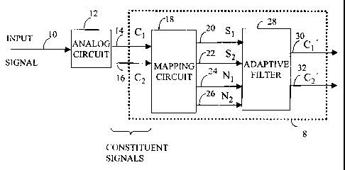
Figure 6 broadly illustrates a signal processor 8 to reduce the undesirable
signal content
in a signal produced by an analog circuit 12 having imperfections. An input
signal 10 is
received by the analog circuit 12. The analog circuit 12 resolves the input
signal 10 into a
constituent signal pair, namely signals CI 14 and CZ 16. Due to the
imperfections in the analog
6
CA 02244446 1998-07-31
circuit 12, relationship between the constituent signals 14,16 is not as
desired. The undesirable
aspects manifest themselves, in the frequency domain, as unwanted spectral
images. These
spectral images degrade the representation of the original input signal 10.
Therefore the effect
of the spectral images resulting from the imperfections in the analog circuit
12 can be
considered noise.
Adaptive filters are routinely used to cancel inband noise in a receive
channel. Echo
cancellers and noise cancellers are typical examples. An aspect of the present
invention
extends the idea of noise to include out of band interferers aliased and or
mixed into the bank
of interest by circuitry imperfections. Used in this application, the adaptive
filter is responsive
to a signal with a small amount of noise and a signal with a large amount of
noise. The
adaptive filter estimates the noise content of the signal and removes it from
the signal, thus
producing an output signal that is much less noisy than the input signal.
An adaptive filter 28 is used to reduce the undesirable signal content caused
by
imperfections in the analog circuit 12. The adaptive filter 28 must be
responsive to a signal
with a small amount of noise and a signal with a large amount of noise.
However, the present
invention is concerned with a pair of related signals, namely C1 14 and CZ 16,
which contain
undesirable signal content. The adaptive filter 28 is therefore responsive to
pairs of signals.
One pair of signals, S, 20 and SZ 22, are signals with a small amount of
noise. The other pair
of signals, Nl 24 and Nz 26, are signals with a large amount of noise. Given
the input of
signals SI 20, SZ 22, Nl 24 and NZ 26 the adaptive filter 28 produces an
output pair of signals,
namely C' ~ 30 and C'2 32, which include a signal with the undesired signal
content from the
analog circuit 12 reduced.
7
CA 02244446 1998-07-31
The required input signals S1 20, Sz 22, ~[ 24 and I~T 26 for the adaptive
filter 28 are
produced by a mapping circuit 18. The mapping circuit 18 is responsive to the
output signal
pair from the analog circuit 12, namely signals C1 14 and CZ 16. The mapping
circuit 18 maps
signals C1 14 and C3 16 to produce signals ~S 20, rS 22, iN 24 andzN 26.
Therefore, the
mapping circuit 18 is responsive to the signal with imperfections produces at
least one signal
with exaggerated undesirable signal content for use by the adaptive filter 28.
Thus, there is provided a signal processor 8 for removing undesirable signal
content in a
signal, namely C, 14 and CZ 16 produced by an analog circuit 12 having
imperfections, the
signal processor 8 comprising: a signal mapping means 18 for exaggerating the
undesirable
signal content; and an adaptive filter means 28 for reducing the undesirable
signal content
using the exaggerated undesirable signal content.
The first component in the signal processor 8 is the signal mapping circuit
18. An
embodiment of the signal mapping circuit 18, which is useful for the
undesirable signal
content for an I,Q system, is shown in Figure 7. The signals C1 14 and CZ 16
which contain
the undesired signal content are fed into a complex filter 38. A complex
filter is a filter that
has a transfer function with complex coefficients. The complex filter 38 maps
signals C1 14
and Cz 16 to signals S, 20 and Sz 22. The mapping accomplished by the complex
filter 38
ensures that signals S, 20 and Sz 22 are suitable for input to the adaptive
filter 28 as the signal
with a small amount of noise.
Signals C1 14 and CZ 16 are also mapped by a second complex filter 40 and
function block
34 to produce signals N, 24 and NZ 26. The mapped signals Nl 24 and Nz 26 are
suitable for
input to the adaptive filter 28 are the signal with a large amount of noise.
Function block 34
exaggerates the undesirable signal content of signals C1 14 and CZ 16. The
transfer function
8
CA 02244446 1998-07-31
of function block 34, f3, is a linear function of input signal ~ 16, and
function block 34
produces output signal 36 for input to complex filter 40:
Filters 38 and 40 often serve to remove direct current (DC) from signals C, 14
and Cz 16,
which is desirable because DC can cause the adaptive filter 28 to not function
as desired. The
filters 38 and 40 can also be used to remove irrelevant signal components
contained in signals
C, 14 and CZ 16. These irrelevant signal components tend to reduce the
effectiveness of the
adaptive filter 28.
Thus, the mapping for the I,Q system shown in Figure 7 is responsive to the
imperfect
signals C, 14 and Cz 16 from analog circuit 18 and produces signals S, 20, SZ
22 and signals
N, 24, NZ 26 suitable for input signals for the adaptive filter 28 with a
small and large amount
of undesirable signal content, respectively.
Figure 8 illustrates another embodiment for the signal mapping circuit 18
which is useful
for the double sampled system. This embodiment is similar to that illustrated
in Figure 7 for
the I,Q system. The difference for the double sampled system illustrated in
Figure 8 is that the
complex filters 38, 40 are replaced by polyphase filters so that the correct
signals S, 20, Sz 22
and signals Nl 24, NZ 26 are provided for the adaptive filter 28.
Thus, the mapping for the double sampled system shown in Figure 8 is
responsive to the
imperfect signals C, 14 and CZ 16 from analog circuit 18 and produces signals
S, Z0, S1 22
and signals N, 24, Nz 26 suitable for input signals for the adaptive filter 28
with a small and
large amount of undesirable signal content, respectively.
Figure 9 illustrates the components comprising the complex filters 38, 40 in
the I,Q
mapping circuit 18 illustrated in Figure 7. The complex filters 38, 40 are
each realized by a
combination of four real filters. The complex filter 38 is realized, in an
embodiment, by four
9
CA 02244446 1998-07-31
real filters 46, 48, 50, 52. Real filters 46 and 52 have the same transfer
function f,a. Real filters
48 and 50 also have the same transfer function f,b. The four real filters 46,
48, 50, 52 are also
cross-coupled. Therefore, the output signal 66 of real filter 50 is subtracted
from the output
signal 62 of real filter 46 by a summation block 78 to produce signal S 1 20.
Also, the output
signal 64 of real filter 48 is added to the output signal 68 of real filter 52
by a summation
block 80 to produce signal Sz 22.
The complex filter 40 is realized, in an embodiment, by four real filters 54,
56, 58, 60.
Real filters 54 and 60 have the same transfer function fza. Real filters 56
and 58 also have the
same transfer fizrlction fzb. The four real filters 54, 56, 58, 60 are also
cross-coupled.
Therefore, the output signal 74 of real filter 58 is subtracted from the
output signal 70 of real
filter 54 by a summation block 82 to produce signal N, 40. Also, the output
signal 72 of real
filter 56 is added to the output signal 76 of real filter 60 by a summation
block 84 to produce
signal Nz 26.
The real filter transfer functions, f,a, f,b, fia and fzb are linear
functions.
Thus, in Figure 9, the complex filters 38,40 are realized to produce the
correct mapping
for the imperfect signals C, 14 and Cz 16 to produce signals S, 20, Sz ZZ and
signals N, 24,
Nz 26 suitable for input signals for the adaptive filter 28 with a small and
large amount of
undesirable signal content, respectively.
Figure 10 illustrates the components comprising the polyphase filters 42,44 in
the double
sampled mapping circuit 18 illustrated in Figure 8. The polyphase filters are
realized in a
similar manner to the complex filters 38,40. The primary difference is the
presence of delay
elements 86 and 90. The output signal 88 of delay element 86 is added to the
output of real
filter 46 by summation block 78 to produce signal S1 20. This is also
different from the
CA 02244446 1998-07-31
realization of complex filter 38 where there was a subtraction of signal 66
from signal 62.
F urther, for polyphase filter 44, the output signal 92 of delay element 90 is
added to the output
of real filter 70 by summation block 82 to produce signal N, 24.
The presence of the delay element 86 is used because the sample represented by
signal 66
is always ahead of the sample represented by signal 62.The presence of the
delay element 90
is used because the sample represented by signal 66 is always ahead of the
sample represented
by signal 62.
Thus, in Figure 10, the polyphase filters 42,44 are realized to produce the
correct mapping
for the imperfect signals C1 14 and CZ 16 to produce signals Sl 20, SZ 22 and
signals Ni 24,
NZ 26 suitable for input signals for the adaptive filter 28 with a small and
large amount of
undesirable signal content, respectively.
Another possible embodiment of the complex filters 38 and 40 for the I,Q
system is
illustrated in Figure 11. In the embodiment shown in Figure 9, function block
34 is in cascade
configuration with real filter 58. Functional block 34 is also in cascade
configuration with real
filter 60. In the embodiment shown in Figure 11, functional block 34 and real
filter 58 are
combined resulting in a real filter 94 with a different linear transfer
function, f4. Similarly, in
the embodiment shown in Figure 11, functional block 34 and real filter 60 are
combined
resulting in a real filter 96 with a different linear transfer function, f5.
Thus, in Figure 1 l, the complex filters 38,40 are realized to produce the
correct mapping
for the imperfect signals C1 14 and CZ 16 to produce signals Sl 20, SZ 22 and
signals N, 24,
Nz 26 suitable for input signals for the adaptive filter 28 with a small and
large amount of
undesirable signal content, respectively.
11
CA 02244446 1998-07-31
Another possible embodiment of the polyphase filters 42 and 44 for the double
sampled
system is illustrated in Figure 12. In the embodiment sho-~n in Figure 10,
function block 34
is in cascade configuration with real filter 58. Functional block 34 is also
in cascade
configuration with real filter 60. In the embodiment shown in Figure 11,
fimctional block 34
and real filter 58 are combined resulting in a real filter 94 with a different
linear transfer
function, f4. Similarly, in the embodiment shown in Figure 11, functional
block 34 and real
filter 60 are combined resulting in a real filter 96 with a different linear
transfer function, f5.
Thus, in Figure 10, the polyphase filters 42,44 are realized to produce the
correct mapping
for the imperfect signals C, 14 and CZ 16 to produce signals S1 20, SZ 22 and
signals Nl 24,
NZ 26 suitable for input signals for the adaptive filter 28 with a small and
large amount of
undesirable signal content, respectively.
Figure 13 illustrates the preferred embodiment of the signal mapping circuit
18. This
embodiment implements a mapping suitable for use with the adaptive filter 28
for both the
I,Q system and the double sampled system.
Considering the general mapping for the I,Q system illustrated in Figure 9,
the preferred
embodiment of Figure 13 is a specific case where the transfer fiznctions fla
and f a for real
filters 46, 52, 54 and 60 are substantially equal to the identity functions.
Furthermore , the
transfer functions fb and f2b for real filters 48, 50, 56 and 58 are
substantially equal to an open
circuit. Thus, since the cross terms are zero, there is no need for summation
blocks 78, 80, 82
and 84 in the preferred embodiment. The transfer function of function block 34
substantially
equal to multiply by negative one.
Considering the general mapping for the double sampled system illustrated in
Figure 10,
the preferred embodiment of Figure 13 is a specific case where the transfer
functions f,a and
12
CA 02244446 1998-07-31
fza for real filters 46, 52, 54 and 60 are substantially equal to the identity
functions.
Furthermore , the transfer functions flb and ~ for real filters 48, 50, 56 and
58 are
substantially equal to an open circuit. Thus, since the cross terms are zero,
there is no need
for summation blocks 78, 80, 82 and 84 or delay elements 86 and 90 in the
preferred
embodiment. The transfer function of function block 34 substantially equal to
multiply by
negative one.
Therefore in both the I,Q system and double sampled systems, the general
embodiments
of the signal mapping circuit 18, illustrated in Figures 9 and 10, reduce to
the same preferred
embodiment of the signal mapping circuit 18 illustrated in Figure 13.
Thus, the signal mapping circuit 18 in Figure 13 provides the correct mapping
for the
imperfect signals C1 14 and Cz 16 to produce signals S~ 20, S~ 22 and signals
I~ 24, I~ 26
suitable for input signals for the adaptive filter 28 with a small and large
amount of
undesirable signal content, respectively.
Turning now to the adaptive filter 28 shown in Figure 6, the preferred
embodiment of the
invention uses a type of adaptive filter known as a noise canceller. Noise
cancellers are well
known in the art of adaptive filters, and therefore are not described in
detail herein.
A N-th order noise canceller 28 is shown in Figure 14, with input signals 20,
22, 24 and
26 and output signals 30 and 32. Elements 113,115,117 and 119 are summers.
Elements 121
and 123 are complex conjugate operators, which often is implemented by
multiplying one of
the components by negative one. Elements 109 and 111 are finite impulse
response (FIR)
filters as are well known in the art. Other forms of filters 109 and 111 are
possible, such as,
recursive, cascade, transposed, and other types well known in the art.
Elements 101 and 103
provide the adaptive coefficient updates for filters 109 and 111. Any adaptive
algorithm can
13
CA 02244446 1998-07-31
be used, however often descent algorithms as are Down in the art are
preferred. The preferred
embodiment of the invention uses least mean squares (LMS) for the adaptive
coefficients
updates, however other algorithms such as gear-shifted LMS, or FRLS could be
used.
Adaptive coefficient updates 101 and 103 produce coefficient vector signals
105 and 107
which control the response of the filters 109 and 111. The coefficient vector
signals 105 and
107 are each N pairs of coefficients, hence the noise canceller is of order N.
A filter in the
signal path within the adaptive filter 28 to block direct current may be
useful.
Although many noise cancellers as are known in the art can be used, the
preferred
embodiment uses a zero order noise canceller with LMS because it is the most
simple
implementation.
A zero order noise canceller used in preferred embodiment of the invention for
the I,Q
system is illustrated in Figure 15. Inputs to the zero order noise canceller
28 are signals 20,
22, 24 and 26. The zero order noise canceller 28 produces output signals 30
and 32. Element
100 is a summer and element 104 is a complex multiplier. Element 110 is a
integration
function and element 112 is a complex square function. Taken together,
elements 110 and
112 implement the LMS in the zero order noise canceller 28. Further the
integration function
110 has a negative gain, however the negative gain could be placed elsewhere
and be
mathematically equivalent. The integration function 110 is in general a
complex integration
to model the phase and gain errors, however a real integration is usually
sufficient for gain
errors only.
In the case of the double sampled system, the preferred embodiment of the
noise canceller
28 is illustrated in Figure 16. Noise canceller 28 is zero order, a specific
case of the general
adaptive filter shown in Figure 14. Inputs to the noise canceller 28 are
signals 20, 22, 24 and
14
CA 02244446 1998-07-31
26, with signals 20 and 24 called the even inputs and signals 22 and 26 called
the odd inputs.
The noise canceller 28 produces output signals 30 and 32. Elements 110 and 144
implement
the LMS algorithm as described previously, except that element 144 is an
amplitude and
phase correction element. Element 144 produces output signal 171 that is
substantially equal
to the power difference of signals 154 and 156. Element 144 also produces
output signal 170
which is a correlation of one of signals 154 and 156 with a derivative of the
other of signals
154 and 156. Integration element 110 is a biphase integrator that integrates
even inputs to get
even outputs and integrates odd inputs to get odd outputs. Summer 166 is also
a biphase
operator that adds even inputs to given even outputs and that add odd inputs
to give odd
outputs. Element 140 is a biphase notch filter that removes the input
component at fs/4.
Finally, element 136 is a biphase multiplier.
Figure 17 illustrated a configuration of a biphase multiplier. The input
signals are 182,
184, 186 and 188. The output signals are 190 and 192. Signals 182, 186 and 190
are called
even signals. Signals 184,188 and 193 are called odd signales. Elements
196,198, 200 and
202 are multipliers. Elements 204 and 206 are summers, and element 208 is a
delay block
multiplied by negative one.
The biphase notch filter is illustrated in Figure 18. Signals 222 and 224 are
the input
signals and signals 226 and 228 are the output signals. Signals 222 and 226
are called even
signals. Signals 224 and 228 are called odd signals. Elements 230 and 232 are
delay blocks
and elements 234 and 236 are summers.
Using the preferred embodiments of the signal mapping circuit 18 and the noise
canceller
28 described above, Figure 19 conceptually illustrates the principles of the
preferred
embodiment of the invention for the I,Q systems. The I and Q signal's
conjugate is taken and
CA 02244446 1998-07-31
run through an adaptive noise cancelling filter and subtracting the result
from the original
signal. In the preferred embodiment the particular adaptive filter technique
used is a LMS
algorithm. The number of taps in the adaptive filter typically required is
small, usually one
or two, making the technique practical.
The preferred embodiment of the invention is implemented as shown in Figure 20
and
combines several existing analog integrated circuits and performs the adaptive
filtering in a
standard Digital Signal Processor and the required decimation in a Field
Programmable Logic
Array (FPGA). This preferred embodiment implementation is a proof of concept
version.
This invention is not restricted to this implementation and can be easily
integrated into any
signal processing engine or mechanism anywhere inside an overall I,Q system.
In fact,
commercial products optimize system partitioning to maximize integration.
In RF receivers using oversampled analog to digital converters in the I,Q
path, this
invention is effective at a decimated sample rate thus simplifying
implementation and
removing the large quantization noise that would normally need to be handled
by the adaptive
filters.
In architectures that use the analog to digital converters to perform the
complex filtering,
such as bandpass sigma delta modulators, this invention corrects for transfer
function
inaccuracies due to mismatch between the analog to digital converters
themselves. Since
complex Bandpass oversampled modulators are particularly sensitive to
mismatch, this ability
to compensate significantly improves performance. Even small mismatches cause
significant
degradation. For example, a 1% mismatch can degrade performance by as much as
35 dB.
The preferred embodiment of this invention has been demonstrated to recover up
to 20dB of
that loss.
16
CA 02244446 1998-07-31
The preferred embodiment of the signal processor in a double sampled system is
shown
in Figure 21. The preferred of the embodiment of the signal mapping circuit is
substantially
the same for the double sampled system as for the I,Q system.
The preferred embodiment of the invention uses a feedforward configuration.
The
feedforward configuration reduces the undesirable signal content in a signal
resulting in a new
signal of higher quality. Another embodiment of the invention may use an
adaptive filter and
associated signal mapping circuit in a feedback configuration. In a feedback
configuration the
adaptive filter and associated signal mapping can be used to reduce the
undesirable signal
content in the output signal from the analog circuit itself.
A further embodiment of the invention can incorporate the signal mapping
circuit into the
adaptive filter circuitry.
A further embodiment of the invention is the double sampled system can use the
same
implementation as in the I,Q system except use the even samples as the input
in place of the
inphase channel and the odd samples as the input in place of the quadrature
channel.
Numerous modifications, variations and adaptations may be made to the
particular
embodiments of the invention described above without departing from the scope
of the
invention, which is defined in the claims.
17