Note: Descriptions are shown in the official language in which they were submitted.
CA 02244466 1998-07-28
W O 97/28002 PCTrUS97/01497
~IG~ RESOLUTION IMAGING ~YSl~M AND METHOD
OF IMA~ING USING THE SAME
Field of the Invention
5The invention is directed to imaging systems and
methods of imaging photosensitive media and the like.
More particularly, the invention is directed to imaging
systems and methods of imaging wherein multiple pixels
are imaged simultaneously.
Bach4lo~d o~ the Invention
Imaging systems are used to create hard copy
visually observable presentations of electronic
information. Example~ include xerographic printers, ink
jet printers, laser, LED and CRT imagers (including
black and white or color, and imaging onto silver halide
media), dye sublimation and wax transfer imagers, among
others. With each type of system there is generally a
computer file which contains representations of
photographic images, artwork, graphics and/or text, and
there is a desire to obtain a paper or film hard copy
from that data.
Electronic production and manipulation of images
and text is highly efficient. Increasingly over time
photographs exist as computer files rather than or in
addition to existing as hardcopies or pieces of film.
The digital environment permits easy retouching and
editing, addition of text and imposition of various
photos into a layout. Moreover, for color photographs,
digital color lookup tables can compensate for
deficiencies in the photographic media and in the
exposure conditions. The existence of images in digital
form therefore creates a need for high quality imaging
systems to create hard copies of these digital images.
Some imaging technologies require the use of light
for the creation of a latent image on a xerographic drum
or silver halide media. One common way of doing this is
to deflect a laser beam with a rotating polygon mirror.
For exposure of color silver halide media, for example,
CA 02244466 1998-07-28
WO 97/28002 PCTrUS97/01497
three lasers are used, one each of (typically) red,
green, and blue. For xerographic applications a single
laser is typically used. The deflected beam is
projected either onto a xerographic drum or onto silver
halide media as appropriate, with the laser beam being
modulated imagewise.
Another common way of creating an image is to
utilize a high-resolution CRT. With a CRT, the black
and white phosphor image is filtered successively with
red, green, and blue filters and imaged onto silver
halide film or paper in order to create an image.
Still another way of creating an image is to
utilize a light valve array to modulate a plurality,
e.g., 64 beams of light emanating from a white light
source (e.g., a short arc xenon lamp) which has been
~iltered. Photographic media is wrapped around a drum
and the image is created in bands, e.g., of 64 pixels
wide.
A commonly sought objective is to increase the
speed of imaging while simultaneously increasing the
resolution and the size of the resultant image.
However, speed, resolution and image size all tend, with
conventional technologies, to be competing objectives
that must be balanced or compromised.
For example, one application ~or imaging
technologies is in point of sale advertisements and
trade show displays, many of which may need to be as
large as 50/' x 100/' or greater. It is desired that the
text be sharp (e.g., often at least 8192 pixels across
the 50" width), even at close viewing distances. It is
desired that the image be created in less than 10
minutes. Both of these objectives, however, cannot be
met or approached by conventional technologies.
Another application is the "package printer" market
which requires that photos, e.g., school portraits, be
imaged at various sizes and with the addition of text
and other graphics. To compete with other processes the
CA 02244466 1998-07-28
W O 97128002 PCT~US97/01497
imaying speed must be about one lineal inch per second.
Again, this is not currently possible with conventional
technologies.
Still another application is the pre-press market,
wherein ~ilms are created ~or later contact printing to
printing plates, or wherein plates are imaged directly.
In order to create high quality hal~tone dots the
resolution must be at least 2,000 dpi, and the ~ilm
width may need to be as much as 50" wide. Such a
capability does not exist with conventional technologies
except at very high cost. Smaller ~ilms are generally
prepared on laser imagers and then reimaged with a step
and repeat imager to create the larger ~ilm. However,
it would be desirable i~ the ultimate film could instead
be imaged in a single step.
It should be appreciated there~ore that the
objectives of large size, high resolution, and rapid
speed are di~icult at best to meet with existing
technologies. In the case o~ the laser imager the
demand o~ larger size requires a greater spacing between
the polygon mirror and the media. The requirement ~or
higher resolution re~uires that this same distance be
reduced -- an objective at odds with the ~irst
requirement. The requirement ~or higher speed requires
that the laser be brighter and that the modulating
device (e.g., an accousto-optic modulator) be ~aster.
However, beyond a certain point this is not possible
with existing technology.
In the case of a CRT imaging system, higher
resolution, up to a point, is obtained by reducing the
intensity o~ the image. Beyond that, however, true
resolutions much greater than 2,000 pixels per screen
are dif~icult to obtain. Moreover, the reduction o~
intensity in order to accomplish smaller spot size and
thus greater resolution is at odds with the objective to
image larger media, which instead requires greater light
levels.
CA 02244466 1998-07-28
W O 97/28002 PCT~US97/01497
In the case o~ a light valve array imaging Bystem/
higher resolution might be obtained by increasing the
number of cells in the light valve array and thus making
each band of image wider. Theoretically, the objectives
of larger size, higher resolution and faster speed can
all be met, but in practice certain problems are
encountered. Most notably, precisely aligning adjacent
image bands is difficult, requiring some degree of
overlapping between the bands. However, in the
overlapping regions, even if alignments and densities
are set perfectly, reciprocity failure of the media can
still cause visible discontinuities between bands.
Reciprocity failure is a complex function of color
and presents a considerable obstacle to system design.
Reciprocity failure is experienced in silver halide
media at very short exposure times. It would be desired
and possibly expected that the media would respond the
same, e.g., to a single burst of light as it would to
two bursts of light each at half the intensity.
However, with short exposure times, (e.g., under a
millisecond) separated by a long time (e.g., on the
order of a second) this is not the case. Moreover, for
color media the phenomenon is quite complex. The amount
of reciprocity failure which is seen in a given layer of
a medium depends on what is happening in other layers.
Potential solutions to reciprocity failure problems
include adjusting exposure according to complex three
dimensional lookup tables, eliminating all overlapping
between pixels ~including scattering within the medium),
or shortening the interval between bursts of light to
well under a second.
Various other methods have been attempted for
accomplishing the high speed, large size, and high
resolution objectives -- many of which involve creating
an image in bands. However, all bandwise imaging
presents both a need to align sections of image
precisely and a need to compensate for reciprocity
CA 02244466 l998-07-28
W O 97f28002 PCTrUS97/01497
~ailure, and to date, no technology has fully addressed
both problems.
There~ore, a substantial need has arisen for an
imaging system offering high speed, large size and high
resolution which does not su~fer ~rom many o~ the
drawbacks associated with conventional technologies
More specifically a need has arisen for an imaging
system which is capable of imaging multiple points
simultaneously while minimizing visible discontinuities
in the resulting image.
Si- ~Y of the Invention
The invention addresses these and other concerns
associated with the prior art in providing an imaging
apparatus which modulates or gates pluralities of light
beams through individual light valves, thereby providing
a greater number and finer resolution o~ modulated light
beams without increasing the number of light valves or
decreasing the spacing between adjacent light valves.
Modulation with the preferred embodiments of the
invention can also be understood to involve a two step
process -- that of jointly modulating entire groups of
light beams and then modulating individual light beams
within each group.
In some pre~erred embodiments, a light generator
incorporating a polygon mirror selectively illuminates
selected bundles o~ ~iber optic strands to selectively
illuminate only a portion o~ a plurality of fiber optic
strands which terminate at any given light valve or
cell, whereby the light generator functions as a
multiplexer or supplemental modulator at the input to
each light valve. Moreover, in other preferred
em~odiments, a composite scan line is created by ganging
a plurality of light valve array modules together side
by side to create a long line o~ image data o~ arbitrary
size and resolution. The scan line may even extend
~ully across an ef~ective imaging area o~ a
CA 02244466 1998-07-28
W097/28002 PCT~S97/01497
photosensitive medium, thereby eliminating the need for
imaging in separate bands or regions.
Therefore, in accordance with one aspect of the
invention, an apparatus is provided for imagewise
exposing photosensitive media. The apparatus includes a
light valve array having a plurality of cells; a
plurality of fiber optic strands having first and second
ends and arranged relative to the light valve array to
illuminate the light valve array through the second
ends, with the second ends of at least two strands
illuminating each cell in the light valve array; and a
light generator selectively illuminating the first ends
of the plurality of fiber optic strands.
In accordance with an additional aspect of the
invention, an apparatus i6 provided for imagewise
exposing photosensitive media. The apparatus includes
light generating means for generating first, second,
third and fourth light beams, the light generating means
including a first modulating means for modulating the
first, second, third and fourth light beams; second
modulating means, having first and second inputs, for
modulating light received at the first and second
inputs; and conveying means for conveying the first and
third light beams from the first modulating means to the
first input of the second modulating means and the
second and fourth modulated light beams from the first
modulating means to the second input of the second
modulating means.
In accordance with another aspect of the invention,.
there is provided a method of imagewise exposing
photosensitive media. The method includes the steps of
generating a plurality of light beams; jointly
modulating groups of light beams from the plurality of
light beams; modulating individual light beams within
each group of light beams to generate a plurality of
output light beams; and conveying the output light beams
to a photosensitive medium to expose an image thereon.
. CA 02244466 l998-07-28
W O 97128002 PCT~US97/01497
These and other advantages and features, which
characterize the invention, are set forth in the claims
annexed hereto and forming a further part hereof.
However, for a better understanding of the invention,
and the advantages and objectives attained by its use,
reference should be made to the Drawing, and to the
accompanying descriptive matter, in which there is
described preferred embodiments of the invention.
Brief ~escri~tion o~ the Drawinq
FIGURE 1 is a functional block diagram of a
preferred imaging apparatus consistent with the
invention.
FIGURE 2 is a functional side elevational view of
the medium transport mechanism in the imaging apparatus
shown in Fig. 1.
FIGURE 3 is a functional top plan view of the light
generating module in the imaging apparatus of Fig. 1.
FIGURE 4 is a functional representation of a
portion of the fiber optic bundles in the imaging
apparatus of Fig. 1.
FIGURE 5 is a functional top plan view of one of
the imaging modules in the imaging apparatus of Fig. 1.
FIGURE 6A is a plan view of the light valve array
~5 in the imaging module of Fig. 5.
FIGURE 6B is an enlarged plan view of a portion of
the light valve array of Fig. 6A, also showing the
relative positions of the fiber optic strands relative
to the cells in the light valve array.
FIGURE 7 is a functional representation of a second
fiber optic array used in the feedback sensor in the
imaging module of Fig. 5.
FIGURE 8 shows several timing diagrams illustrating
a preferred sequence of imaging for the imaging
apparatus of Fig. 1.
CA 02244466 1998-07-28
W O 97128002 PCTrUS97/01497
Detailed De~criPtion o~ the Preferred Embodiment~
In pre~erred embodiments o~ the invention, a common
light generating module, or light generator, generates a r
plurality o~ light beams which are modulated in groups
5 and then conveyed to one or more imaging modules which
then modulate the individual light beams within the
groups.
The preferred light generator utilizes a light
source to generate a primary light beam which is
10 re~lected o~ o~ a spinning polygon mirror to one of a
plurality o~ bundles o~ fiber optic strands. As the
polygon mirror rotates, each o~ the ~iber optic bundles
is sequentially illuminated.
The other end o~ this array o~ ~iber optic bundles
15 is brought to the surface of a light valve array which
has a plurality of cells so that individual fiber optic
strands may illuminate designated cells. Each o~ the
bundles accessed by the polygon mirror has one strand
brought out within the active region o~ each light valve
2Q cell, with the ends o~ the ~ibers being arranged to ~orm
a more or less linear array. A portion o~ the strands
terminating at each light valve cell may overlap
spatially with other strands in other cells, thereby
reducing the e~ective number o~ strands per cell.
For example, in one preferred embodiment, 20 ~iber
optic bundles are provided, which are connected to a
light valve array including 64 cells staggered into two
rows, thereby orienting 20 strands proximate each cell.
With four o~ the strands overlapping spatially with
other strands in other cells, an effective width of 16
strands is provided in each cell, and the array o~ ~iber
optic strands may be considered to include 16 bundles.
In this con~iguration, the ~irst bundle would have
strands directed at scan lines #1, 17, 33, etc., the
second bundle would have strands directed at scan lines
~2, 18, 34, etc., the third bundle would have ~ibers
directed at scan lines ~3, 19, 35, etc., and so on.
CA 02244466 1998-07-28
W O 97/28002 PCTrUS97/01497
Thus each cell in the light valve array would control 16
pixels in the image. Compared to the alternative of
providing one light valve cell ~or each pixel, this is
~ar less expensive and ~ar more reliable.
Moreover, pre~erred embodiments o~ the invention
may utilize a plurality o~ imaging modules, arranged in
a side-by-side manner, to provide a longer e~ective
scan line. This may have the bene~it o~ imaging the
entire width o~ a photosensitive media without resorting
to imaging in multiple bands. Continuing with the above
example, i~ four imaging modules are arranged side-by-
side, a total o~ 4098 pixels (4 modules x 64
cells/module x 16 pixels/cell) may be imaged within the
same scan line.
Turning now to the Drawing, wherein like numbers
denote like parts throughout the several views, Fig. 1
shows a pre~erred imaging apparatus 10 consistent with
the principles of the present invention. Apparatus 10
generally includes a light generator 20 coupled to a
plurality o~ imaging modules 60, 62, 64 and 66 through
an array o~ ~iber optic strands ~0 having ~irst ends 51
coupled to the light generator and second ends 52
coupled to the imaging modules.
A controller 11 coordinates the activities o~ the
light generator and the imaging modules to output a scan
line 68 o~ image data onto a photosensitive medium. A
plurality o~ light beams are output ~rom imaging module
60 and are ~ocused by an optical system (e.g., lens 61
to image a portion 68a o~ scan line 68 onto the
photosensitive medium. Similarly, imaging modules 62,
64 and 66 output light beams which are ~ocused by lenses
63, 65 and 67 to image portions 68b, 68c and 68d o~ scan
line 68.
A ~ine adjustment in the alignment o~ the various
modules is pre~erably provided so as to align the
portions to ~orm a contiguous scan line that is
substantially free o~ any discontinuities between the
CA 02244466 1998-07-28
W O 97/28002 PCT~US97/01497
scan line portions. Adjustment and alignment o~ the
imaging modules is important. Each module there~ore
pre~erably includes means ~or adjusting its respective
lens ~e.g., lens 61 ~or module 60) to be closer to or
farther ~rom the photosensitive medium to obtain correct
focus and magnification, in a similar manner as
adjusting the focus on a camera. Each module also
pre~erably has means for adjusting its portion o~ the
scan line up or down (i.e., in a direction perpendicular
1~ to the axis o~ the scan line). This is preferably a
screwdriver adjustment on the entire module which allows
it to tilt slightly.
The re~;n'ng adjustment which is pre~erably
provided ~or the imaging modules is that o~ correcting
separation from module to module. Each module is
preferably mounted to a track which allows it to slide
closer or further away ~rom adjoining modules. Between
each of the modules is a wedge which may be moved by a
screwdriver adjustment so as to push the modules ~urther
2~ apart or closer together. At each end o~ the entire
assembly o~ modules is a spring and a fixed stop,
positioned so as to ~orce the modules closer to each
other, restricted only by the wedges which separate the
modules.
It will be appreciated that other mechanisms may be
utilized to provide any o~ the above-listed adjustments
~or the imaging modules. Moreover, certain adjustments
may not be required in some applications.
The modules are pre~erably adjusted as follows. A
test pattern is imaged which is alternating groups of
two pixels ~ully on and two pixels ~ully of~. In place
of a silver halide medium, however, a hard copy linear
ruling at the same ~requency (two pixels on, two pixels
o~f) is placed in the image plane in the region where
scan line portions (e.g., portions 68a and 68b) join.
The pattern is precisely aligned so that a portion o~ it
inter~eres with a portion of region 68a, with pixels
CA 02244466 1998-07-28
W O 97/280~2 PCTrUS97/01497
11 '
which are on falling on black lines and pixels which are
off aligning to white lines. The result is a generally
dark region, except that if the ruling is slightly
misaligned the region is much brighter. This alignment
being done, the alignment of the adjoining module is
adjusted until the same darkness is seen in the area
which it images. This method is preferably used because
it produces a rather large visual indication of small
misalignments, thus permitting more precise alignment.
In the preferred embodiment, the photosensitive
medium is a photosensitive film 18 such as a silver
halide film that is supported on the surface of a drum
12. Film 18 typically includes an imaging area 19 that
represents the active photosensitive area of the film
upon which it is desired to form an image. The imaging
area may include the full width of the film, or there
may be a border area on either or both edges of the
film. Other photosensitive media, including other films
as well as photosensitive drums, may also be used
consistent with the invention.
Fig. 2 illustrates the preferred medium transport
mechanism in apparatus 10 for moving the photosensitive
medium relative to scan line 68 imaged through the
aforementioned optical systems (only one of which,
optical system 67 for imaging module 66, is shown in
Fig. 2). In the preferred embodiment, a roll-to-roll
medium transport mechanism is utilized, where a
photosensitive film 18 (e.g., a 12" wide roll of color
silver halide film such as Kodak Supra II or Konica QA
negative acting color paper) is supplied by supply roll
15 and taken up by take-up roll 16, both driven by bi-
directional motors (not shown). The motors are
controlled so as to maintain the tension in the media at
a constant level via dancer rollers 13 and 14. The
paper is wrapped around capstan or drum 12 which is
turned at a constant rate by a stepping motor and worm
drive (functionally illustrated at 17). After imaging,
CA 02244466 1998-07-28
W O 97128002 PCT~US97/01497
12
the roll o~ ~ilm may be removed from take-up roll 16,
placed in a black bag, carried to a processor, and
processed chemically to yield a color image.
Numerous other medium transport mechanisms may be
incorporated consistent with the invention. For
example, the medium transport may rotate only a
photosensitive drum which transfers an image to paper as
in a laser printer. Further, imaging may be performed
on a flat bed, rather than a drum or similar support.
~0 In general, the type of transport will be dictated by
the type of medium imaged and the particular handling
requirements of this medium.
Re~erring next to Fig. 3, light generator 20 is
shown in greater detail. A primary light beam 22 i8
created in light generator 20 by a light source 30 which
includes a 150 watt short arc xenon lamp 31, such as an
Optical Radiation Corporation US~150-1 lamp. This lamp
dissipates about half of the total energy within a
sphere of 0.5 mm diameter, and has a color temperature
which is uniform throughout its li~e. Alternate light
sources, including another lamp, a laser, a laser diode
or a light emitting diode, among others, may be used in
the alternative.
The intense nearly point source o~ light generated
by lamp 31 is imaged by a first lens assembly (including
lenses 32 and 33) onto a first aperture on a ~irst
opaque member 35. Items 32 and 33 are pre~erably Edmund
~cienti~ic G32,971, 50 mm diameter 50 mm ~ocal length
plano convex coated lenses. Opaque member 35 preferably
lncludes a .75 mm diameter aperture to eliminate any
unwanted light (i.e., light well outside the central .5
mm sphere in the lamp). An infrared absorbing filter 34
may also be used to minimize the thermal buildup in
other parts of the system and remove an unwanted
infrared portion of the spectrum.
A color wheel 40 is preferably interposed in the
optical path of primary light beam 22, pre~erably
.
CA 02244466 1998-07-28
W O 97/28002 PCTrUS97/01497
13
between the lamp and the first opaque member, and is
driven by a hysteresis synchronous motor 42. As this
color wheel rotates at high speed (e.g., about 6,000
rpm) the light entering the first aperture is filtered
to be red, green, or blue. A shutter 44, driven by a
stepping motor 46, may be used to rapidly turn all light
on or ofE. Shutter 44 is preferably an opaque vane with
a 3 mm hole which may align or not align with the first
aperture, depending on the position o~ stepping motor
46. The shutter is use:Eul when data is lacking to start
a new print, or when data becomes lacking during the
imaging of a print.
Primary light beam 22, after passing through opaque
member 35 and shutter 44, is preferably ~ocused by a
second lens assembly (including lens 36, preferably an
Edmund Scientific G45,082: 9 mm diameter, 9 mm ~ocal
length) onto the surface at the ~irst end 51 of fiber
optic array 50. The shape o~ the beam is restricted by
a second aperture formed in a second opaque member 37.
This aperture is preferably in the shape of a
vertically-oriented slit, restricting the width but not
the height o~ the beam which is imaged on the face of
fiber optic array 50. The position of the beam on fiber
optic array 50 is controlled by a motor and polygon
mirror assembly 45. Motor and polygon mirror assemblies
are available from a number of sources, including
Lincoln Laser Co. of Phoenix, AZ.
Lens 36 is preferably selected and positioned such
that the image of the .5 mm sphere generated by lamp 31
is enlarged about 5x. As restricted by the preferred
second aperture, the image of the primary light beam at
end 51 of fiber optic array 50 (a rectangular face of
fibers) is about O.ln high and about 0.05/' wide.
Motor-Polygon mirror assembly 45 spins rapidly
about its axis, e.g., pre:Eerably at about 11,250 RPM, to
successively and sequentially direct primary light beam
22 onto sections in fiber optic array 50. While only 20
CA 02244466 1998-07-28
W O 97f280~2 PCT~US97/01497
14
lines are shown as fiber optic array 50 in Fig. 3, this
should be interpreted as 20 sections (or bundles)
arranged into a row, each section (corresponding to one
line) being 16 fiber strands wide and 16 fiber strands
high. The fiber optic strands are each preferably about
0.0025" in diameter, so each of the 20 sections is about
0.04l' wide (scan direction) and about 0.04" tall (cross-
scan direction). As a greater number of fibers may be
provided in the cross-scan direction in other
embodiments, provision is made for more than 16 fibers
tall to be illuminated.
It should be appreciated, therefore, that light
generator 20 operates as a first modulator ~or
modulating light to the groups or bundles of ~iber optic
strands 50, thereby jointly modulating the plurality of
light beams formed within each ~iber optic bundle.
Moreover, since the light generator operates to
sequentially illuminate each bundle, the light generator
may be considered to operate as a multiplexer o~ sorts
for routing light to one of a plurality o~ bundles. In
general, any light producing mechanism that is capable
o~ providing one or more modulated light beams (either
sequentially or non-sequentially, singularly or in
groups~ to a secondary modulation unit (e.g., a light
~alve cell used in the preferred light valve arrays) may
be used consistent with the invention.
Alternative embodiments may use alternative light
sources other than a short arc xenon lamp, an
alternative number of fiber optic strands per cell,
and/or an alternative number of cells. Moreover, the
filter wheel may not be used i~ only black and white
imaging is to be performed. Moreover, other means may
be used for switching the light from fiber optic bundle
to bundle, e.g., a self-resonant galvo mirror, an analog
galvo mirror, or shutters, and the light modulation may
be sequential or non-sequential (i.e., random access),
with multiple or single bundles illuminated at a time.
CA 02244466 l998-07-28
W O 97~8002 PCTrUS97/01497
Individual bundles may also be illuminated by separate
light sources, e.g., la9er diodes or light emitting
diodes. Other modifications to the light generator may
be made consistent with the invention.
Turning briefly to Fig. 5, illumination module 60
is shown in greater detail to il~ustrate the connection
of the module to light generator 20. Modules 62, 64 and
66 are similarly configured. In particular, a portion
of fiber optic array 50 is supported at second end 52 by
a fiber optic block 82 to illuminate a light valve array
70 sandwiched between a pair of polarizers ~4, 86. The
pre~erred light valve array includes 64 light valve
cel~s arranged in two rows. With this configuration,
individual light valve cells within the array are
capable of modulating the light conveyed by one of the
strands positioned proximate the cells. The modulated
llght beams output from this arrangement are directed to
optical system 61 to be focused on the photosensitive
medium as discussed above. With this configuration,
light valve array 70 ~unctions as a second modulator ~or
modulating the individual light beams from each bundle
o~ fiber optic strands, resulting in a two-step
modulation process when operating in conjunction with
light generator 20. A ~eedback sensor 90 (discussed
below~ is also interposed between the light valve array
and the optical system to regulate the intensities o~
the individual light valve cells in the array.
The fiber optic array is preferably con~igured to
route one strand from each bundle to each light valve
cell. As an illustration, a functional diagram o~ the
routing of ~iber optic strands ~rom light generator 20
to imaging module 60 is shown in Fig. 4. Only four rows
of fibers are shown at ends 51, with the other twelve
rows in the 16 x 16 arrangements o~ ~ibers within each
bundle being omitted for clarity, as they are routed to
imaging modules 62, 64 and 66 in a similar manner as
will be discussed below.
CA 02244466 l998-07-28
W 097/2~002 PCT~US97/01497
16
The array o~ fiber optic strands is preferably
constructed using a programmable winder. The fibers may
be wound on a slowly rotating drum over a release liner.
A computer controlled leadscrew then controls the place
where the fiber i8 released to lie on the drum, and
grooved guides insure that the fibers lie in the
correct locations. Two assemblies may be wound back to
back, symmetrically. Once an assembly is finished a
thin layer of epoxy may be applied to hold the ~ibers
together. Once this is cured the assembly may be cut
apart and epoxied together with similar other
assemblies. A~ter the epoxy hardens the assemblies may
then be cut and polished as necessary.
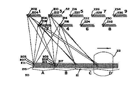
Returning to Fig. 4, at ~irst end 51, the ~iber
optic strands are arranged into the row of bundles
(numbered A, B, C, D, etc.), while at second end 52 the
strands are arranged into groups (numbered 1, 2, 3, 4,
5, 6, 7, 8, 9, etc.), with each group illuminating a
separate cell in light valve array 70.
The ~irst ends (the ends illuminated by light
generator 20) o~ a portion of the ~ibers in bundles A
and B are numbered with odd numbers 203 through 217.
The other ends (those which illuminate the various cells
of the light valve array) are numbered by even numbers
one less than that which indicates the illuminated end.
~he primary light beam 22 moves along this array to
illuminate all ~ibers. Then as the polygon mirror
rotates to bring a next ~acet into illumination, the
gc~nn;ng process is repeated.
The sc~nn;ng sequence resulting from the sequential
illumination of bundles A, B, C, D, etc. is to ~irst
illuminate the leftmost fiber o~ each cell, e.g., 202,
2~}6, 210, 214, 218, 222, 226, 230 and 234 (respectively
in groups 1-9). Shortly thereafter the second fiber of
each cell (e.g., 204, 208, 212, 216, 220, 224, 228, 232
and 236 ~or groups 1-9) is illuminated, and so on until
all 20 ~ibers ~or each cell have been illuminated.
CA 02244466 l998-07-28
W 0971280~2 PCTrUS97/01497
17
Light valve array 70 iS shown in greater detail in
Figs. 6A and 6B. AS shown in Fig. 6A~ light valve array
70 iS pre~erably a chip approximately 0.6" x 1 ~n in
size of P~ZT material, such as Motorola Ceramic Products
type 9065 material. This material is prei~erably about
O.025~ thick and is placed between two sheets oE
polarizing filters (numbered 84 and 86 in Fig. 5~. The
electrodes are thin layers of nichrome and gold, vapor
coated and etched to form the illustrated pattern. The
f~irst polarizing filter (numbered 84 in Fig. 5) has an
axis ~45- relative to the axis o~ the array, and the
second polarizing ~ilter (numbered 86 in Fig. 5) is +45-
relative to the axis, such that the two polarizing
~ilters are crossed and thus normally blocking nearly
all light. When a voltage iB applied between a common
electrode 72 and any cell electrode, e.g., electrode 73
the piezoelectric nature of the PLZT material causes
stress to occur within the material. Inasmuch as the
material is also birefringent, the vector o~ polarized
light rotates. Over the range o~ zero volts to
approximately 450 volts (the hal~wave voltage ~or this
configuration), the light transmitted for a given cell
varies ~rom that o~ two polarizers crossed (less than
0.1~ of the incident light) to that o~ two parallel
polarizers (about 272;-). Electrical connections to the
chip are made near its edge 71. Wide areas in the
electrode traces allow more easy connection to a printed
circuit board, by zebra strips, wire bonding, or heat
seal tape (a 3M product), among others.
An enlarged view oi~ a portion oi~ light valve array
70 iS shown in Fig. 6B, with groups 1-9 oE ~iber optic
array 50 shown in positions suitable ~or illuminating
the individual light valve cells (i.e., they are
positioned at the inputs o~ the light valve cells).
Fiber ends 202, 206~ 210~ 214~ 218, 222/ 226~ 230 and
234 f~or groups 1-9 which also appear in Fig. 2 can be
seen as being the ~irst ~iber in each o~ the first nine
CA 02244466 1998-07-28
W O 97/28002 PCTrUS97/01497
18
cells. Electrode ends 73-81, together with common
electrode 72, ~orm the individual light valve cells.
The fibers illuminate the active region o~ each cell,
this being generally the regions between the electrodes
73-81 and common electrode 72.
As shown in Fig. 6A, the light valve array includes
two rows o~ 32 cells each, with the even numbered cells
(those in the second row) staggered to be oriented hal~-
way along the scanning or imaging axis between the
separation between adjacent odd numbered cells (those in
the ~irst row). Moreover, the strands within the groups
that illuminate each light valve cell are arranged into
two rows o~ 10 strands each, with those in the second
row staggered half-way between those in the ~irst row.
The 1024 pixels o~ image (64 cells x 16 ~ibers/cell
-- as ~our of the ~ibers in each cell are overlapping)
created by each imaging module are in ~our lines which
extend along an imaging axis (i.e., generally oriented
along the longitudinal axis o~ the drum, and similarly
along the direction o~ the common electrode in the light
valve array) and which are spaced apart vertically
~perpendicular to the longitudinal axis o~ the drum, and
to the direction o~ the common electrode in the light
valve array). The purpose o~ having two rows o~ ~ibers
per cell is to eliminate gaps between pixels and
maximize the use~ulness o~ each light valve cell. The
purpose o~ having cells on both sides o~ the array
common electrode 72 is to eliminate short circuiting
between cells. Cells cannot be made to join each other.
The vertical separations caused by having two rows o~
~ibers per cell and having cells on both sides o~ the
array common is compensated ~or in the data delivery to
~orm a contiguous scan line, so the image on the media
does not show any indication o~ the image having been
made in any discontinuous m~nn~r. In ~act, the slight
delay in time (i~ any) between cells on opposite sides
o~ the array common electrode a~ter data delivery
CA 02244466 1998-07-28
W O 97/28002 PCT~US97/01497
19
compensation is below the time interval required for
reciprocity failure.
Further, as discussed above, in the preferred
imaging apparatus 10, 1024 pixels are imaged by each
imaging module. Thus, to create a 12" wide image at 300
dpi, 3600 pixels are required, and consequently four
imaging modules 60, 62, 64, 66 are preferably used side
by side. With four modules, 4096 pixels are created,
and the resolution depends on the size of image created
by each module which, in turn, depends on the
speci~ications and placement o~ lenses 61, 63, 65 and
67. Pre~erably each of the four imaging modules images
a 3" wide line (portions 68a, 68b, 68c and 68d), so the
resolution at the media is 341 ppi (pixels per inch).
Returning to Fig. 5, feedback sensor 90 is
interposed between light valve array 70 and optical
system 61 for imaging module 60. It should be
appreciated that similar ~eedback sensors may be
incorporated into the other imaging modules, or that a
2~ single ~eedback sensor may control all imaging modules.
A beamsplitter 91 de~lects part o~ the output light
beams generated by imaging module 60 towards a mirror
92, through lens 93, and onto a second fiber optic array
95 which has ~ace 94. The other end o~ these fibers is
delivered to each of 64 photodiodes e.g., photodiode 97,
which are mounted on a printed circuit board 96.
While the output of each cell is primarily a
function o~ the voltage applied to each cell electrode
le.~., electrode 73), this output will also depend on
the intensity o~ lamp 31, the quality o~ the polish on
the ends of each ~iber within array 50, the amount of
space charge accumulated by each cell i~ any, and the
temperature of the PLZT material, among other ~actors.
To eliminate such uncertainty in the light output, the
light from each of the 64 cells is sampled at ~ace 94
and delivered to the photodiodes on board 96. These
photodiodes are in a feedback circuit which regulates
CA 02244466 1998-07-28
W O 97/28002 PCT~US97/01497
the voltage to each cell to obtain the desired light
output.
Second fiber optic array 95 i6 illustrated in
greater detail in Fig. 7. The origin of light is from
the first ends of fibers such as fiber 98, being
arranged patternwise the same as light valve array 50.
The destination of light in each fiber is a point on a
printed circuit board containing a corresponding
photodiode, such as photodiode 97. If the photodiodes
were small enough to be arranged patternwise the same as
the light valve array this fiber optic cable would not
be necessary. However, since that is generally not the
case some way to convey light to these photodiodes is
required, and this fiber optic cable arrangement
accomplishes that. For the sake of clarity, only some
of the fiber optic connections from end to end are
illustrated, even though the actual part would have all
such connections made.
Returning to Fig. 1, controller 11 coordinates the
activities of light generator 20 and imaging modules 60,
62, 64 and 66 to image scan lines on the photosensitive
medium. Further, this controller also coordinates the
activation of the medium transport so that multiple scan
lines may be imaged across the medium to ~orm an image
thereupon.
The sequence of imaging a scan line with imaging
apparatus 10 is illustrated by timing diagrams 101, 102
and 103 in Fig. 8. For purposes of simplicity it is
assumed in this figure that there is just one sweep of
the polygon mirror for red, one for green, and one ~or
blue. Then this process is repeated. However, color
negative paper is generally much less sensitive to red
than it is to green, and less sensitive to green than it
is to blue light. Thus, to m~; m; ze the use of the
available dynamic range of light within each color, two
modifications should be made. First, three sweeps of
red should be made for every single sweep of green and
CA 02244466 1998-07-28
W O 97/28002 PCTrUS97/01497
21
blue, and second, the neutral density of the blue layer
in the color wheel should be made to be less than that
- o~ the other two colors.
Except for the fact that the duplication of red
sweeps is not indicated in Fig. 8, however, timing
diagram 101 does illustrate which color is being
projected onto the ~ace o~ the fiber optic array 50
during imaging. Timing diagram 103 shows which of the
20 fibers in each light valve cell (e.g., fiber 202 or
204 for cell #1) is primarily illuminated. It is
understood that there is some overlap, i.e., for a time
both fibers #n and #n+1 will be illuminated. This will
result in some blurring between adjacent scan lines.
However, this is normal, expected, and desired ~or
imagers. Such blurring minimizes the visibility of scan
lines in the resultant image.
Timing diagram 102 shows which data is applied to
the light valve cells, i.e., for which of the 20 fibers.
The data applied while fibers #1, #2, #19 and #20 are
illuminated is "Blank", i.e., the cells are turned off.
The purpose ~or these end cells can be more easily
understood by considering the case of not having any end
fibers, but rather only the sixteen internal ~ibers,
numbered #3 through #18. When data is first applied to
:Eiber #3 in actuality the sc~nn;ng beam is only
partially illuminating this Eiber. Fiber #3 being only
dimly illuminated at this instant of time, the
photodiode (e.g., 97) senses a reduced light intensity
and raises the voltage to that cell to compensate. This
is undesirable, in that ~iber #3 behaves di~erently
from fiber #4. As data is first applied to fiber #4,
~iber #3 is also partially illuminated. The sum o~
illumination amounts ~or ~ibers #3 and #4 together at
that instant is approximately the same as it is a short
time later when only fiber #4 is illuminated. The
~eedback photodiode properly adjusts the voltage to the
cell over this time. Moreover, as the light leaves
CA 02244466 1998-07-28
W O 97/28002 PCT~US97/01497
22
fiber #4 and moves to ~iber #5 the same is true, namely
that the photodiode senses the true cell activity, even
though it may receive this in~ormation via more than one
~iber. Now, going back to ~iber ~3, as soon as non-
blank data is enabled ~or this cell it is desired thatthe photodiode respond at that instant in a way similar
to the way it will respond when the scanning beam is
centered on i~iber #3. This i8 accomplished by having
the adjoining ~iber #2 also illuminated. Similarly, at
the end of the sweep fiber ~19 is illuminated so as to
again not con~use the photodiode. I~ no photodiodes
were used for feedback, ~ibers #1, ~2, #19 and #20 would
not be needed and would not be required.
While only 18 fibers are required to accomplish
greater stability of the ~eedback, the additional two
fibers at the ends make the fiber assembly easier
inasmuch as adjoining rows o~ fibers are symmetrical.
It is characteristic of polygon mirrors that there
is a region of time when two mirror facets are
illuminated, and the sc~nn;ng beam is split in two
directions. Normally this is an undesirable situation.
However, in the case o~ this pre~erred embodiment the
position of fiber optic bundle 50 is ad~usted relative
to the polygon mirror 45 so as to avoid split beam
sc~nn;ng only for the central 16 fibers. I~ the
scanning beam is partially but minim~lly split when the
end fibers are illuminated this is not o~ great
consequence.
Returning again to ~ig. 1, in a ~ashion well known
to those skilled in the art, data is received by
controller 11 ~rom a host computer and bu~fered in a
band buffer At the same time data elsewhere within
this band buffer is separated into red, green, and blue
components, o~fset to compensate ~or spatial dif~erences
between even and odd numbered fibers and even and odd
numbered cells, selected according to the current color
and fiber being imaged, and conveyed to digital to
CA 02244466 l998-07-28
W O 97128002 PCTrUS97/01497
23
analog converters which in turn drive high voltage
drivers for each cell in each imaging module. Also in
- the data flow, just prior to the high voltage drivers,
is a lookup table which compensates ~or variations
between driver circuits and sensing photodiodes.
~ ith this preferred embodiment the ~ollowing
numerical in~ormation is relevant:
The speed o~ the polygon mirror is pre~erably about
11,250 rpm. With its 8 facets, it therefore scans at
about 1,500 scan lines/second.
The color wheel pre~erably has three sections, each
section including 3 wedges o~ red and one each o~ green
and blue. Edge wedge occupies 1/15 of a circle or 24
degrees. The color wheel turns at about 6,000 rpm, and
with its 15 wedges per circle it thus moves through
1,500 wedges per second, thus changing colors at times
which match the starts o~ new sweeps by the polygon
mirror. The sequence o~ colors ~or a given scan line o~
data is pre~erably red, green, blue, red, red. By
imaging the green and blue data approximately midway
between red images the displacement between images ~or
each o~ the three colors is minimized. If this were not
the case some means ~or displacing the data slightly
would most likely need to be employed. The rotation o~
the filter wheel is pre~erably linked and synchronized
to the rotation o~ the polygon mirror, thus assuring
proper timing o~ the transitions in colors.
Moreover, given that 5 color wedges are pre~erably
utilized per scan line o~ data, the imaging speed is
1500/5 = 300 scan lines per second.
Under these imaging conditions, the dwell time on a
single ~iber is about 1/12 o~ 1/1500 second, or about 55
microseconds. This is adequate time for data to be sent
to each o~ the 64 cells, and this is reasonable ~or
operation with photodiode feedback. Typically
photodiode-op amp combinations have a response time of
4-8 microseconds, and this is well below the 55
CA 02244466 1998-07-28
W O 97/28002 PCT~US97/01497
24
microsecond pixel time. The light valves can respond in
well under a microsecond, and are thus not a problem.
Their speed is determined almost entirely by the speed
of their respective high voltage driver.
As discussed above, in the preferred imaging
apparatus there is one light generator and multiple
imaging modules. Duplications of ~iber optic array 50
within the light generator are stacked one on top of
another so that all are scanned simultaneously. Recall
that this fiber optic array is 4 fibers high ~or each
imaging module. If there are ~our imaging modules, as
there are in this preferred embodiment, then :Eace 51 i8
16 ~ibers high. Given that the beam size is or can be
made taller, eight, or any other number of imaging
modules can be easily accommodated.
The pixelwise separation between the two adjacent
rows of ~ibers within each cell, and between the even
and odd numbered cells, is preferably compensated ~or by
varying the placement of data into a buffer memory.
Re~erring again to Fig. 6B, the various rows o~ er
optics may be envisioned at an instant of time
coincident with pixel row~ #1, #2, #8 and #9. At a
later instant in time these same fibers are coincident
with pixel rows #2, ~3, #9 and #lO, etc. Whether the
total spatial separation is 8 pixels or a greater or
fewer number of pixels depends on the relative speed o~
the medium relative to the scan line.
Data received from a host computer is preferably
buffered within memory circuits associated with each
module, wherein in one section data is being written
while in another section data is being read for imaging.
Data is placed in this memory, e.g., O, l, 7 or 8 pixel
rows advanced o~ a nominal pixel position. Thus when
the data is later retrieved a correction has been made
~or these spatial differences. The timewise delay in
imaging of various pixels is still short enough (a few
CA 02244466 1998-07-28
W O 97/28002 PCTAUS97/01497
milliseconds) such that reciprocity ~ailure does not
occur.
Various modifications may be made to the preferred
embodiments without departing from the spirit and scope
o~ the invention. For example, as a second pre~erred
embodiment, the number of imaging modules may be changed
~rom four to eight, and the width imaged by each imaging
module may be increa5ed to about 6.875n. With this
configuration, a 50" wide roll of media may be imaged at
about 148.9 dpi. The imaging speed may remain at about
300 scan lines/second, thereby producing a lineal
imaging speed o~ about two inches per second. This
would permit a 50" x 100" point of sale advertisement to
be imaged in less than one minute. For highly
insensitive media, e.g., display film, the lineal speed
may also be reduced and the data ~low rate adjusted to
compensate. In other words, the vertical and horizontal
resolutions may be made to be different from each other.
Black and white Thermal Dry Silver media (such as
is available ~rom 3M Co.) may also be imaged at high
resolution with a third pre~erred embodiment o~ the
invention. In this embodiment, no color wheel would be
required. Each facet of the polygon mirror would image
a separate line o~ image, so the imaging speed would
become about 1,500 scan lines/second. The size o~ the
fiber optic strands may be reduced ~rom 0.0025" to
0.00125", and the number o~ cells per PLZT chip, may be
decreased ~rom 64 to 32, so the number o~ ~iber optic
strands per cell is increased from 20 to 80, o~ which 64
are non-overlapping. Each imaging module would then
project 2048 pixels. Thirty-two modules may be used to
obtain a total pixel count o~ 65,536. To provide a
resolution of 2,048 pixels per inch, the maximum medium
width would be 32". Binary data ~each pixel being
either black or white) may be rasterized at 9,600 dpi
and processed in groups o~ 4 x 4 pixels. The number of
black pixels within this grid may be counted and used to
CA 02244466 1998-07-28
W O 97/28002 PCTrUS97/01497
26
establish one of 17 grayshades, a means of resolution
enhancement commonly practiced within this art. The
medium may be advanced at the rate of about 1,500/2048 =
0.73 inches per second. Consequently, a 32" x 40" pre-
press film or printing plate may ~e imaged in 54seconds.
As a fourth preferred embodiment, the number of
cells per imaging module may be made to be sixteen, with
thirty two fibers used per module, spaced at an interval
1/15 that of the spacing between cells. The last ~iber
in one cell may be spatially coincident, in the
direction perpendicular to the scan line, with the first
fiber in the next cell. No other fibers would be needed
or used. With this embodiment, the same data would be
used to control the last fiber in one cell as would be
used to control the spatially coincident fiber in the
next cell.
The change from 64 cells, as used in the first
preferred embodiment, to 32 cells has the advantage that
fewer drivers would be needed and thus the cost would be
reduced. It has the disadvantage, however, that the
response time required per fiber would be twice as fast.
The voltages sent to cells may be controlled by a
single re~erence voltage, which is slowly (i.e., over 27
microseconds, the preferred imaging time ~or each fiber)
and linearly switched from zero to a certain reference
voltage during the time that the first fiber within a
given module is illuminated. The voltage may later be
slowly and linearly switched from that reference voltage
to zero during the time that the last fiber is
illuminated. Thus, pixels imaged by those ~ibers would
be imaged twice, first by a first ~iber in one cell and
second by a last fiber in another cell. The ramping up
and ramping down of the reference voltage may also be
made to occur at a rate and timing so as to maintain
stability of the feedback circuitry during this time.
CA 02244466 1998-07-28
W O 97/28002 PCTrUS97101497
27
This change from the first preferred embodiment has
the advantage that the timing required for turn-on and
turn-off may be quite slow, and thus the demands on the
electronic design may be eased, and/or the circuitry may
be made to operate at higher scan rates, such as is
re~uired by changi~g from 16 to 32 active fibers per
cell as is done in this embodiment. This change also
has the advantage that no fibers other than the active
fibers would be required. This embodiment, however, has
the disadvantage that additional complexity in the data
control circuitry may be required to direct the data for
each last fiber for a cell to also be the data for the
first fiber in each next cell.
A ~ifth preferred embodiment may be configured
similarly to the third preferred embodiment, except that
light source 31 may be implemented using a helium neon
laser. A sixth preferred embodiment may also be
configured for black and white imaging o~ graphic arts
film, using 64 fibers per cell and 32 cells per module.
However, all of the items shown in Fig. 3 in the optical
path ~rom lamp 31 through polygon mirror 45 may be
eliminated, with each bundle of ~ibers in array 50 being
illuminated instead by a separate individually-modulated
light source such as laser diode or light emitting
diode. The light sources may be switched so as to
sequentially or selectively illuminate associated fibers
or groups o~ fibers. Unlike the disclosed con~iguration
with the polygon mirror, there would be no retrace time
when no ~ibers were ~ully illuminated. Inasmuch as each
light source would be turned on for only a very short
time, each light source could operate at a much higher
power level than it could if it were operated
continuously.
In addition, in any of the above-described
pre~erred embodiments a lower cost, albeit with lower
image ~uality, may be obtained by eliminating the
~eedback photodiodes (e.g., 97) and their associated
CA 02244466 1998-07-28
W O 97/28002 ~CTrUS97/01497
28
components. This may be especially appropriate when an
imager is creating halftone dots, where most of the time
cells are either fully on or fully of~, and there is
less need ~or precise regulation o~ intensities.
As will be appreciated ~rom the above discussion,
numerous other modi~ications may be made to tailor an
imaging apparatus to any particular application.
In summary, in the pre~erred embodiments each
imaging module may accomplish a resolution that would
normally take many more light valves using conventional
imaging technologies. For example, with the ~irst
pre~erred embodiment discussed above, the resolution
which would otherwise be achieved with 1024 light valve
cells and 1024 driver circuits is realized using only 64
cells and 64 drivers. This results in substantial
savings in the cost o~ production, as well as increased
reliability.
In prior art imagers a polygon mirror is generally
thought o~ as scanning a single beam across the width o~
the media. In the pre~erred embodiments, however, a
polygon mirror may be considered to sweep hundreds of
beams, each across a small distance (0.046" in the first
pre~erred embodiment). In prior art imagers both the
polygon mirror and the focusing lens must be a
substantial distance from the media, and thus any wobble
in its bearings or vibration o~ the system can cause
displacement o~ the scan lines. In the pre~erred
embodiments, however, the behavior of the polygon mirror
is not critical. Moreover, the ~ocusing lens is a short
distance ~rom the media, thus achieving high resolution
at low cost.
Many other configurations will be apparent to those
skilled in the art. For example, the imaging modules
may be movable in a cross-scan direction to provide
band-wise imaging. Moreover, the scanning and cross-
gc~nn;ng directions may be reversed with respect to the
photosensitive medium. In ~act, practically any method
CA 02244466 1998-07-28
W O 97/28002 PCTrUS97/01497
29
o~ scanning an image on a photosensitive medium may be
modi~ied to incorporated the benefits of pre~erred
embodiments of the invention. As other modi~ications
will be appreciated by one skilled in the art, the
invention therefore lies in the claims hereinafter
appended.