Note: Descriptions are shown in the official language in which they were submitted.
CA 02244692 1998-08-OS
-1-
TEMPERATURE COMPENSATED CURRENT MEASUREMENT DEVICE
BACKGROUND OF THE INVENTION
This invention relates to current shunts for measuring
current in a circuit.
A current shunt is essentially a low value resistance
element connected in a circuit as a means of sensing a
measuring current. For measuring high currents, the
resistance element may simply be a strip of metallic
conductor with voltage sensing points at each end and a
defined resistance between the two voltage sensing points.
The current flowing through the shunt is calculated by
measuring the voltage drop across the shunt, that is,
between the two voltage sensing points, and dividing the
voltage by the resistance of the shunt. A copper shunt
suffers from a large change in resistance due to
temperature. A significant current measurement error
occurs if a fixed value for resistance is used in the
calculation of the current through such a shunt.
Typically, this error is large, as much as 35 percent over
0 degrees Celsius to 100 degrees Celsius. In the prior
art, this effect is overcome by using a more expensive
material such as manganin instead of copper, the manganin
having a much smaller change in resistance with
temperature.
The use of a separate, more expensive material, obviously
adds expense to the measurement device, but also adds
mechanical connections between existing circuit components
and the more expensive material. The addition of
mechanical connections, increases resistance and increases
susceptibility to problems due to corrosion, oxidation,
mechanical fatigue and the like.
It would be desirable, therefore, to sense current through
an existing circuit component without the need for
CA 02244692 2004-03-O1
-2-
additional mechanical connections, and without the need
for a more expensive material with a small resistance-
temperature coefficient. The present invention addresses
this need.
BRIEF SU1~'ARY OF THE INVENTION
In accordance with one aspect of the invention, there is
provided an apparatus for measuring current. The
apparatus includes a conductive shunt for developing a
voltage drop due to current flow therethrough, a low
noise input network connected to the conductive shunt, a
fixed gain amplifier connected to the low noise input
network to amplify the voltage drop to produce a current
signal representing current flow through the conductive
shunt and an attenuator connected to the amplifier to
attenuate the current signal, the attenuator including a
temperature sensor for sensing temperature of the shunt
and connected to the fixed gain amplifier such that the
current signal is attenuated by an amount dependent upon
temperature of the shunt.
The conductive shunt may have a resistance which
increases with temperature of the resistance and the
attenuator may attenuate the current signal generally
proportionally to an increase in temperature of the
resistance.
The temperature sensor may include a negative temperature
coefficient thermistor.
The conductive shunt may include a solid copper strip.
CA 02244692 2004-03-O1
-3-
The attenuator may include a voltage divider including
the negative coefficient thermistor.
The voltage divider may include first and second
resistances and the negative coefficient thermistor
connected in series.
In accordance with another aspect of the invention, there
is provided a method of measuring current. The method
involves developing a voltage drop across a conductive
shunt, applying the voltage drop to a low noise input
network connected to a fixed gain amplifier, amplifying
the voltage drop with the fixed gain amplifier to produce
a current signal representing current flow through the
conductive shunt and attenuating the current signal by an
amount dependent upon temperature of the shunt to
compensate the current signal for changes in the voltage
drop across the shunt due to the known dependence of the
shunt upon temperature.
BRIEF DESCRIPTION OF THE SEVERAh VIEWS OF THE DRAWING
In drawings which illustrate embodiments of the invention,
Figure 1 is a schematic diagram of an apparatus,
according to a first embodiment of the
invention; and
Figure 2 is a perspective view of a conductive shunt
according to the first embodiment of the
invention.
CA 02244692 1998-08-OS
-4-
DETAINED DESCRIPTION OF THE INVENTION
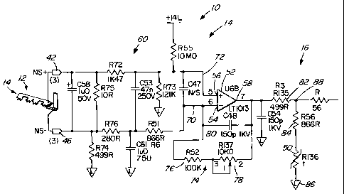
In accordance with a first embodiment of the invention is
shown generally at 10. The apparatus includes a copper
conductive member shown generally at 12, a differential
amplifier shown generally at 14 and a voltage divider shown
generally at 16.
Conductive Shunt
Referring to Figure 2, the conductive member is shown
generally at 12. The conductive member has a first portion
disposed in a first plane and has a second portion 17
disposed in a second plane at right angles to the first
plane. The first portion has first, second, third and
fourth finger portions 18, 20, 22 and 24 and has first,
15 second and third rivet holes 26, 28 and 30. The finger
portions are for connection to switching transistors (not
shown) and the rivet holes are for mounting the member to
a circuit board 31. The member 12 is secured to a printed
circuit board 31 using the rivet holes 26, 28 and 30.
Circuit board pads are provided under adjacent respective
rivet holes such that the member makes contact with the
pads connected by traces to components on the circuit
board, the components including those of the differential
amplifier 14 and voltage divider 16 shown in Figure 1.
The member further includes a right angled strip of
material which acts as a shunt 32 which extends between the
first and second portions 15 and 17. The second portion 17
has a first rivet hole 34 and the resistance of the shunt
32 is measurable between the rivet holes 30 and 34.
The second portion of the conductive member has an opening
38 to which a bus bar may be connected for conduction of
high current, through the second portion 17 through the
shunt 32, and into the first portion 15.
CA 02244692 1998-08-OS
_5_
A first circuit board trace 40 extends from a circuit pad
under and in contact with rivet hole 30 to a first input
terminal 42 of the amplifier shown in Figure 1. Referring
back to Figure 2, a second circuit board trace 44 extends
from the pad under rivet hole 34 to a second terminal 46 of
the amplifier shown in Figure 1. Thus, the shunt is
connected between the first and second input terminals 42
and 46 of the amplifier 14.
Referring back to Figure 2, the circuit board 31 has a
signal ground trace 47 having a termination pad 48 on which
the rivet hole 34 rests. Thus, this point of the
conductive member is at ground potential. A thermistor 50
has a case which is soldered directly to the second portion
17 and is therefore in thermal conduction with the second
portion 17 and at the same potential as the second portion
that is, ground potential.
As the second portion 17 is part of the same piece of
copper forming the shunt 32, these portions are in thermal
conduction with each other and therefore the temperature of
portion 17 is representative of the temperature of the
shunt 32. A temperature measured by the thermistor 50 is
thus the temperature of the shunt 32.
Current flowing through the resistive portion 32 produces
a voltage drop between the rivet holes 30 and 34 which act
as voltage sense points. It will be appreciated that the
effective resistance of the shunt 32 varies in relation to
temperature, and therefore, the voltage drop between the
rivet holes 30 and 34 also varies with temperature.
The variance of resistance due to temperature is given in
the prior art as:
a (T2-25)
CA 02244692 1998-08-OS
-6-
Where: a is a constant for the material under
consideration, in this embodiment
0.0043;
T2 is the operating temperature of the
resistance portion; and
25 is a standard temperature in degrees
Celsius.
Thus, the absolute resistance of the resistance portion is
given as
R2-R25 [1+a(t2 -25)l
Where: R2 is the resistance at the operating
temperature;
T2 is the operating temperature of the
resistance portion;
R25 is the resistance at 25o Celsius; and
a in this embodiment is 0.0043.
Thus, the effective resistance of the shunt 32 has a known
dependence on temperature and therefore, it may be said
that the voltage drop across the shunt has a known
dependence upon the temperature of the shunt.
Thermistor
In this embodiment, the thermistor is a negative
temperature coefficient thermistor having a tolerance of 5
percent. The specific thermistor used in this embodiment
is manufactured by Keystone under part number RL2006-1600-
103-D1. In this embodiment, the thermistor has a
resistance which varies inversely proportional with
temperature.
Differential Amplifier
In this embodiment, the differential amplifier includes an
operational amplifier 52 having an inverting input 54, a
non-inverting input 56 and an output 58. In this
embodiment, the operational amplifier is an LT 1013
CA 02244692 1998-08-OS
manufactured by Motorola Inc. The differential amplifier
includes an input network 60 having first and second input
terminals 62 and 64 to which are connected circuit board
traces 40 and 44 shown in Figure 2, which are connected to
the first and second voltage sense points 30 and 34
respectively. The input network is a low noise input
network and has outputs 70 and 72 which are connected to
the inverting and non-inverting inputs 54 and 56 of the
operational amplifier 52, respectively.
The differential amplifier further includes a feedback path
74. The feedback path includes a fixed resistor 76, an
adjustable resistor 78 and a filter capacitor 80. The
fixed resistor 76 and adjustable resistor 78 are connected
in series across the inverting input 54 and the output 58,
and act in cooperation with the input network 60 to cause
the differential amplifier to have a gain, which in this
embodiment, is approximately 1000. Thus, in response to a
voltage drop of approximately 1 mV across the rivet holes
30 and 34, the output 58 of the operational amplifier
produces a signal having a voltage level of approximately
1.0 volt. The adjustable resistor 78 provides for
adjustment of the gain for calibration of the differential
amplifier 14.
Voltage Divider
Still referring to Figure l, the voltage divider includes
first and second fixed precision resistors 82 and 84
respectively. In this embodiment, these resistors have
values of 499 ohms and 866 ohms respectively. Referring to
Figure 2, a first lead wire 49 of the thermistor 50 is
connected to a circuit pad 51 which is connected to the
second resistor 84 through a circuit board trace 53. The
case of the thermistor is connected to signal ground
through a connection to the second portion 17 and the rivet
hole 34. Thus, the first resistor, the second resistor and
the thermistor are connected in series. Referring back to
CA 02244692 1998-08-OS
_g_
Figure 1, an output 88 of the voltage divider is provided
at a circuit node between the first and second resistors 82
and 84. Thus, the voltage divider 16 acts a voltage
divider including the negative coefficient thermistor.
A voltage signal of approximately 0.6 volts is provided at
the output 88, in response to a 1 mV voltage drop across
the rivet holes 30 and 34. Effectively, the differential
amplifier 14 and the voltage divider 16 act as an amplifier
circuit for amplifying the voltage drop across the shunt by
an amount dependent upon the temperature of the shunt, to
compensate for changes in the voltage drop across the shunt
due to the known dependence of the shunt resistance upon
temperature.
Operation
Referring to Figures 1 and 2, at an ambient temperature of
approximately 25 degrees Celsius, with no current flowing
through the first portion 15, the thermistar 50 presents a
nominal resistance to the voltage divider 16 and a voltage
of 0 volts is provided at the output 88, as no current is
flowing through the copper bar.
When current flows through the shunt 32, a voltage is
developed thereacross, this voltage being developed between
the rivet holes 30 and 34. The voltage appearing across
these points is amplified by the differential amplifier 14
and the instantaneous temperature of the bar due to the
current flowing through it and ambient conditions, causes
the thermistor 50 to present a new resistance to the
voltage divider 16. Assuming the current through the
effective resistance creates heating of the resistive
portion 32, the resistance produced by the thermistor 50 is
reduced from its nominal value and therefore, a lesser
resistance is presented to the voltage divider 16.
CA 02244692 1998-08-OS
_g_
At the same time, as the temperature of the shunt 32
increases, the voltage drop between the rivet holes 30 and
34 increases. Therefore, a signal having a higher than
nominal voltage level appears at the output 58 of the
operational amplifier 52 however, the thermistor in the
voltage divider 16 increases the attenuation of the signal
appearing at the output 58 of the operational amplifier 52
due to the lesser resistance presented by the thermistor
50. This compensates for the increase voltage drop across
the rivet holes 30 and 34, due to temperature. A reverse
effect occurs as the resistive portion cools.
The signal appearing at the output 58 of the operational
amplifier 52 varies by perhaps 35 percent over a
temperature range of 0 to 100 degrees Celsius. However,
after the signal passes through the temperature compensated
voltage divider 16, the signal appearing at output 88
varies by about plus or minus 2 percent over the same
temperature range. This is equivalent to or better than
the accuracy provided with conventional shunts such as
Manganin shunts, and therefore, avoids the need to use
materials with small resistance temperature coefficients.
In addition, as copper is commonly the preferred choice for
conductive members such as conductive bus bars and the like
in power circuits, current measurement of current flowing
through such bus bars can be made relatively accurately,
without the need to make a separate mechanical connection
to a material having a low resistance temperature
coefficient, in series with the copper bus bar. Only one
mechanical connection to the shunt is required. This at
least minimizes the number of mechanical connections and
minimizes problems associated with mechanical connections,
which includes potentially high resistance, oxidation
problems, fatigue, etc.
CA 02244692 1998-08-OS
-10-
While specific embodiments of the invention have been
described and illustrated, such embodiments should be
considered illustrative of the invention only and not as
limiting the invention as construed in accordance with the
accompanying claims.