Language selection

Search

Patent 2244720 Summary

Third-party information liability

Some of the information on this Web page has been provided by external sources. The Government of Canada is not responsible for the accuracy, reliability or currency of the information supplied by external sources. Users wishing to rely upon this information should consult directly with the source of the information. Content provided by external sources is not subject to official languages, privacy and accessibility requirements.

Claims and Abstract availability

Any discrepancies in the text and image of the Claims and Abstract are due to differing posting times. Text of the Claims and Abstract are posted:

  • At the time the application is open to public inspection;
  • At the time of issue of the patent (grant).
(12) Patent: (11) CA 2244720
(54) English Title: CHARGE SENSITIVE AMPLIFIER WITH HIGH COMMON MODE SIGNAL REJECTION
(54) French Title: AMPLIFICATEUR REAGISSANT A LA CHARGE ET CAPABLE D'UN TAUX ELEVE D'ELIMINATION DU SIGNAL EN MODE COMMUN
Status: Expired and beyond the Period of Reversal
Bibliographic Data
(51) International Patent Classification (IPC):
  • H03F 03/45 (2006.01)
  • H03F 01/22 (2006.01)
  • H03F 03/345 (2006.01)
(72) Inventors :
  • COLBETH, RICHARD E. (United States of America)
  • ALLEN, MAX J. (United States of America)
  • MALLINSON, MARTIN (Canada)
(73) Owners :
  • VARIAN MEDICAL SYSTEMS, INC.
(71) Applicants :
  • VARIAN MEDICAL SYSTEMS, INC. (United States of America)
(74) Agent: R. WILLIAM WRAY & ASSOCIATES
(74) Associate agent:
(45) Issued: 2002-01-22
(86) PCT Filing Date: 1997-11-13
(87) Open to Public Inspection: 1998-06-04
Examination requested: 1998-07-28
Availability of licence: N/A
Dedicated to the Public: N/A
(25) Language of filing: English

Patent Cooperation Treaty (PCT): Yes
(86) PCT Filing Number: PCT/US1997/020872
(87) International Publication Number: US1997020872
(85) National Entry: 1998-07-28

(30) Application Priority Data:
Application No. Country/Territory Date
08/758,538 (United States of America) 1996-11-29

Abstracts

English Abstract


A charge sensitive amplifier with high common mode signal rejection includes
an NPN bipolar junction transistor (BJT) and a P-channel metal oxide
semiconductor field effect transistor (MOSFET) connected in a totem pole
circuit configuration. The BJT base terminal receives a dc reference voltage,
the MOSFET gate terminal receives the incoming data signal, the MOSFET drain
terminal is grounded and the BJT collector terminal provides the output
voltage signal and is biased by the power supply through a resistive circuit
element. The MOSFET operates as a source follower amplifier with the
transconductance of the BJT serving as the load at the source terminal, while
the BJT operates as a common emitter amplifier with the transconductance of
the MOSFET providing emitter degeneration. The signal gains of such source
follower and common emitter amplifiers are substantially equal and of opposite
polarities. Therefore, any common mode signal components due to common mode
input signals present at the input terminals (i.e., the BJT base and MOSFET
gate terminals) which would otherwise appear within the output signal are
substantially cancelled, thereby resulting in a high degree of common mode
signal rejection.


French Abstract

La présente invention concerne un amplificateur réagissant à la charge et capable d'un taux élevé d'élimination du signal en mode commun, et qui comporte, d'une part un transistor bipolaire à jonction ou "BJT" (bipolar junction transistor) de type NPN, et un transistor MOSFET à canal P, lesquels transistors sont montés en circuit à totem pôle. La borne de la base BJT reçoit une tension de référence, la borne de grille du MOSFET reçoit le signal de données entrant, la borne de drain du MOSFET est mise à la masse, et la borne collecteur du BJT, qui donne le signal en tension de sortie, est polarisée par l'alimentation électrique au moyen d'un élément à circuit résistant. Le MOSFET travaille comme amplificateur à source suiveuse lorsque la transconductance du BJT sert de charge à la borne source, le BJT travaillant comme amplificateur à émetteur commun lorsque la transconductance du MOSFET assure la contre-réaction de l'émetteur. Les gains de signal d'une telle source suiveuse et des amplificateurs à émetteur commun sont sensiblement égaux et de polarités opposées. Il en résulte la suppression sensiblement totale de toutes les composantes de signal du mode commun correspondant à des signaux d'entrée du mode commun présents au niveau des bornes d'entrée (c'est-à-dire les bornes base du BJT et grille du MOSFET) qui, sinon, se manifesteraient dans le signal de sortie. L'invention permet ainsi un taux élevé d'élimination du signal en mode commun.

Claims

Note: Claims are shown in the official language in which they were submitted.


The embodiments of the invention in which an exclusive
property or privilege is claimed are defined as follows:-
1. An apparatus including a charge sensitive amplifier with high common mode
signal rejection, said charge
sensitive amplifier comprising:
a current controlled transistor circuit configured to receive a do input
reference with a common mode input
signal and in accordance therewith provide a first common mode signal
component, wherein a ratio of said
first common mode signal component to said common mode input signal equals a
first signal gain;
a voltage controlled transistor circuit, coupled to said current controlled
transistor circuit, configured to
receive a data input signal with said common mode input signal and in
accordance therewith provide a data
signal component and a second common mode signal component, wherein a ratio of
said second common
mode signal component to said common mode input signal equals a second signal
gain; and

an output circuit, coupled to one or both of said current and voltage
controlled transistor circuits, configured
to receive and combine said data signal component and said first and second
common mode signal
components and in accordance therewith provide an output signal which
corresponds to said data input
signal, wherein a ratio of said output signal to said data input signal
substantially equals said second signal
gain;
wherein said data input signal is single-ended and said do input reference and
said data input signal are
unrelated to one another;
wherein said first and second signal gains are substantially equal and of
opposite polarities and said first and
second common mode signal components substantially cancel one another; and
wherein said current and voltage controlled transistor circuits are coupled
together in a totem pole circuit
configuration.
2. The apparatus of claim 1, wherein said current controlled transistor
circuit includes a first semiconductor
output region of a first conductivity type from which said first common mode
signal component is provided,
said voltage controlled transistor circuit includes a second semiconductor
output region of a second
conductivity type from which said data signal component and said second common
mode signal component
are provided, and said first and second conductivity types are of opposite
conductivity types.
3. The apparatus of claim 2, wherein said current controlled transistor
circuit comprises an NPN bipolar
junction transistor and said voltage controlled transistor circuit comprises a
P-channel metal oxide
semiconductor field effect transistor.
4. The apparatus of claim 2, wherein said current controlled transistor
circuit comprises a PNP bipolar
junction transistor and said voltage controlled transistor circuit comprises
an N-channel metal oxide
semiconductor field effect transistor.
5. An apparatus including a charge sensitive amplifier with high common mode
signal rejection, said charge
sensitive amplifier comprising:
a current controlled transistor circuit configured to receive a do input
reference with a common mode input
signal and in accordance therewith provide a first common made signal
component, wherein a ratio of said
first common mode signal component to said common mode input signal equals a
first signal gain;
a voltage controlled transistor circuit, coupled to said current controlled
transistor circuit, configured to
receive a data input signal with said common mode input signal and in
accordance therewith provide a data
signal component and a second common mode signal component, wherein a ratio of
said second common
mode signal component to said common mode input signal equals a second signal
gain; and
an output circuit, coupled to one or both of said current and voltage
controlled transistor circuits, configured
to receive and combine said data signal component and said first and second
common mode signal
components and in accordance therewith provide an output signal which
corresponds to said data input
signal, wherein a ratio of said output signal to said data input signal
substantially equals said second signal
gam;
wherein said data input signal is single-ended and said do input reference and
said data input signal are
unrelated to one another;

wherein said first and second signal gains are substantially equal and of
opposite polarities and said first and
second common mode signal components substantially cancel one another; and
wherein said current and voltage controlled transistor circuits are coupled
together in an opposing circuit
configuration and said output signal comprises a differential output signal
with first and second opposing
signal phases provided by said current and voltage controlled transistor
circuits, respectively.
6. The apparatus of claim 5, wherein said current controlled transistor
circuit includes a first semiconductor
output region of a conductivity type from which said first common mode signal
component is provided and
said voltage controlled transistor circuit includes a second semiconductor
output region of said conductivity
type from which said data signal component and said second common mode signal
component are provided.
7. The apparatus of claim 6, wherein said current controlled transistor
circuit comprises a PNP bipolar
junction transistor and said voltage controlled transistor circuit comprises a
P-channel metal oxide
semiconductor field effect transistor.
8. The apparatus of claim 6, wherein said current controlled transistor
circuit comprises an NPN bipolar
junction transistor and said voltage controlled transistor circuit comprises
an N-channel metal oxide
semiconductor field effect transistor.
9. The apparatus of claim 5, wherein said output circuit comprises a plurality
of circuit elements exhibiting
a plurality of circuit resistance characteristics.
10. An apparatus including a bipolar and metal oxide semiconductor charge
sensitive amplifier with high
common mode signal rejection, said charge sensitive amplifier comprising:
a bipolar junction transistor (BJT) configured to receive a do input reference
with a common mode input
signal and in accordance therewith provide a first common mode signal
component, wherein a ratio of said
first common mode signal component to said common mode input signal equals a
first signal gain;
a metal oxide semiconductor field effect transistor (MOSFET), coupled to said
BJT, configured to receive a
data input signal with said common mode input signal and in accordance
therewith provide a data signal
component and a second common mode signal component, wherein a ratio of said
second common mode
signal component to said common mode input signal equals a second signal gain;
and
a resistive output circuit, coupled to one or both of said BJT and said
MOSFET, configured to receive and
combine said first and second common mode signal components and said data
signal component and in
accordance therewith provide an output signal which corresponds to said data
input signal, wherein a ratio
of said output signal to said data input signal substantially equals said
second signal gain;
wherein said data input signal is single-ended and said do input reference and
said data input signal are
unrelated to one another;
wherein said first and second signal gains are substantially equal and of
opposite polarities and said first and
second common mode signal components substantially cancel one another; and
wherein said BJT and said MOSFET are coupled together in a totem pole circuit
configuration.

11. The apparatus of claim 10, wherein said BJT includes a first semiconductor
output region of a first
conductivity type from which said first common mode signal component is
provided, said MOSFET
includes a second semiconductor output region of a second conductivity type
from which said data signal
component and said second common mode signal component are provided, and said
first and second
conductivity types are of opposite conductivity types.
12. The apparatus of claim 11, wherein said BJT comprises an NPN BJT and said
MOSFET comprises a
P-channel MOSFET.
13. The apparatus of claim 12, wherein said BJT comprises a PNP BJT and said
MOSFET comprises an
N-channel MOSFET.
14. An apparatus including a bipolar and metal oxide semiconductor charge
sensitive amplifier with high
common mode signal rejection, said charge sensitive amplifier comprising:
a bipolar junction transistor (BJT) configured to receive a dc input reference
with a common mode input
signal and in accordance therewith provide a first common mode signal
component, wherein a ratio of said
first common mode signal component to said common mode input signal equals a
first signal gain;
a metal oxide semiconductor field effect transistor (MOSFET), coupled to said
BJT, configured to receive a
data input signal with said common mode input signal and in accordance
therewith provide a data signal
component and a second common mode signal component, wherein a ratio of said
second common mode
signal component to said common mode input signal equals a second signal gain;
and
a resistive output circuit, coupled to one or both of said BJT and said
MOSFET, configured to receive and
combine said first and second common mode signal components and said data
signal component and in
accordance therewith provide an output signal which corresponds to said data
input signal, wherein a ratio
of said output signal to said data input signal substantially equals said
second signal gain;
wherein said data input signal is single-ended and said dc input reference and
said data input signal are
unrelated to one another;
wherein said first and second signal gains are substantially equal and of
opposite polarities and said first and
second common made signal components substantially cancel one another; and
wherein said BJT and said MOSFET are coupled together in an opposing circuit
configuration and said
output signal comprises a differential output signal with first and second
opposing signal phases provided by
said BJT and MOSFET, respectively.
15. The apparatus of claim 14, wherein said BJT includes a first semiconductor
output region of a
conductivity type from which said first common mode signal component is
provided and said MOSFET
includes a second semiconductor output region of said conductivity type from
which said data signal
component and said second common mode signal component are provided.
16. The apparatus of claim 15, wherein said BJT comprises a PNP BJT and said
MOSFET comprises a
P-channel MOSFET.
17. The apparatus of claim 15, wherein said BJT comprises an NPN BJT and said
MOSFET comprises an

N-channel MOSFET.
18. A method of amplifying a charge sensitive signal with high common mode
signal rejection, said method
comprising the steps of:
receiving a do input reference with a common mode input signal and in
accordance therewith generating a
first common mode signal component with a current controlled transistor
circuit, wherein a ratio of said first
common mode signal component to said common made input signal equals a first
signal gain;
receiving a data input signal with said common mode input signal and in
accordance therewith generating a
data signal component and a second common mode signal component with a voltage
controlled transistor
circuit, wherein said current and voltage controlled transistor circuits are
coupled together in a totem pole
circuit configuration and a ratio of said second common mode signal component
to said common mode
input signal equals a second signal gain; and
combining said first and second common mode signal components and said data
signal component and in
accordance therewith generating an output signal which corresponds to said
data input signal, wherein a
ratio of said output signal to said data input signal substantially equals
said second signal gain:
wherein said data input signal is single-ended and said dc input reference and
said data input signal are
unrelated to one another; and
wherein said first and second signal gains are substantially equal and of
opposite polarities and said first and
second common mode signal components substantially cancel one another.
19. The method of claim 18, wherein:
said step of receiving a dc input reference with a common mode input signal
and in accordance therewith
generating a first common mode signal component with a current controlled
transistor circuit comprises
receiving said dc input reference with said common mode input signal and in
accordance therewith
generating said first common mode signal component with said current
controlled transistor circuit
including a first semiconductor output region of a first conductivity type
from which said first common
mode signal component is provided;
said step of receiving a data input signal with said common mode input signal
and in accordance therewith
generating a data signal component and a second common mode signal component
with a voltage controlled
transistor circuit comprises receiving said data input signal with said common
mode input signal and in
accordance therewith generating said data signal component and said second
common mode signal
component with said voltage controlled transistor circuit including a second
semiconductor output region of
a second conductivity type from which said data signal component and said
second common mode signal
component are provided; and
said first and second conductivity types are of opposite conductivity types.
20. The method of claim 19, wherein:
said step of receiving a dc input reference with a common mode input signal
and in accordance therewith
generating a first common mode signal component with a current controlled
transistor circuit comprises
receiving said dc input reference with said common mode input signal and in
accordance therewith

generating said first common mode signal component with an NPN bipolar
junction transistor; and
said step of receiving a data input signal with said common mode input signal
and in accordance therewith
generating a data signal component and a second common mode signal component
with a voltage controlled
transistor circuit comprises receiving said data input signal with said common
mode input signal and in
accordance therewith generating said data signal component and said second
common mode signal
component with a P-channel metal oxide semiconductor field effect transistor.
21. The method of claim 19, wherein:
said step of receiving a dc input reference with a common mode input signal
and in accordance therewith
generating a first common mode signal component with a current controlled
transistor circuit comprises
receiving said dc input reference with said common mode input signal and in
accordance therewith
generating said first common mode signal component with a PNP bipolar junction
transistor; and
said step of receiving a data input signal with said common mode input signal
and in accordance therewith
generating a data signal component and a second common mode signal component
with a voltage controlled
transistor circuit comprises receiving said data input signal with said common
mode input signal and in
accordance therewith generating said data signal component and said second
common mode signal
component with an N-channel metal oxide semiconductor field effect transistor.
22. A method of amplifying a charge sensitive signal with high common mode
signal rejection, said method
comprising the steps of:
receiving a dc input reference with a common mode input signal and in
accordance therewith generating a
first common mode signal component with a current controlled transistor
circuit, wherein a ratio of said first
common mode signal component to said common mode input signal equals a first
signal gain;
receiving a data input signal with said common mode input signal and in
accordance therewith generating a
data signal component and a second common mode signal component with a voltage
controlled transistor
circuit, wherein said current and voltage controlled transistor circuits are
coupled together in an opposing
circuit configuration and a ratio of said second common mode signal component
to said common mode
input signal equals a second signal gain; and
combining said first and second common mode signal components and said data
signal component and in
accordance therewith generating an output signal which corresponds to said
data input signal, wherein a
ratio of said output signal to said data input signal substantially equals
said second signal gain;
wherein said data input signal is single-ended and said dc input reference and
said data input signal are
unrelated to one another;
wherein said first and second signal gains are substantially equal and of
opposite polarities and said first and
second common mode signal components substantially cancel one another; and
wherein said output signal comprises a differential output signal with first
and second opposing signal
phases provided by said current and voltage controlled transistor circuits,
respectively.
23. The method of claim 22, wherein:

said step of receiving a dc input reference with a common mode input signal
and in accordance therewith
generating a first common mode signal component with a current controlled
transistor circuit comprises
receiving said dc input reference with said common mode input signal and in
accordance therewith
generating said first common mode signal component with said current
controlled transistor circuit
including a first semiconductor output region of a conductivity type from
which said first common mode
signal component is provided; and
said step of receiving a data input signal with said common mode input signal
and in accordance therewith
generating a data signal component and a second common mode signal component
with a voltage controlled
transistor circuit comprises receiving said data input signal with said common
mode input signal and in
accordance therewith generating said data signal component and said second
common mode signal
component with said voltage controlled transistor circuit including a second
semiconductor output region of
said conductivity type from which said data signal component and said second
common mode signal
component are provided.
24. The method of claim 23, wherein:
said step of receiving a dc input reference with a common mode input signal
and in accordance therewith
generating a first common mode signal component with a current controlled
transistor circuit comprises
receiving said dc input reference with said common mode input signal and in
accordance therewith
generating said first common made signal component with a PNP bipolar junction
transistor; and
said step of receiving a data input signal with said common mode input signal
and in accordance therewith
generating a data signal component and a second common mode signal component
with a voltage controlled
transistor circuit comprises receiving said data input signal with said common
mode input signal and in
accordance therewith generating said data signal component and said second
common mode signal
component with a P-channel metal oxide semiconductor field effect transistor.
25. The method of claim 23, wherein:
said step of receiving a dc input reference with a common mode input signal
and in accordance therewith
generating a first common mode signal component with a current controlled
transistor circuit comprises
receiving said dc input reference with said common mode input signal and in
accordance therewith
generating said first common mode signal component with an NPN bipolar
junction transistor; and
said step of receiving a data input signal with said common mode input signal
and in accordance therewith
generating a data signal component and a second common mode signal component
with a voltage controlled
transistor circuit comprises receiving said data input signal with said common
mode input signal and in
accordance therewith generating said data signal component and said second
common mode signal
component with an N-channel metal oxide semiconductor field effect transistor.
26. The method of claim 2, wherein said step of combining said first and
second common mode signal
components and said data signal component and in accordance therewith
generating an output signal which
corresponds to said data input signal comprises combining said first and
second common mode signal
components and said data signal component and in accordance therewith
generating said output signal
which corresponds to said data input signal with a plurality of circuit
elements exhibiting a plurality of
circuit resistance characteristics.

Description

Note: Descriptions are shown in the official language in which they were submitted.


CA 02244720 l998-07-28
W O98/24176 - PCT~US97/20872
CEL~R G~ SENSrll~E A M PLlFnER WIlla
E~GH COMMON MODE SIGNAL REJl~CTION
l~lk;LD OF TEIE ~NVENTION
The present invention relates to charge sens;Live am--plifiers~ and in particular, to charge
S sensitive amplifiers with dirrerel"ial input t~rmin~l~ and high com~non mode signal rejection.
BACKGROUND OF THE INVENTION
Charge sensitive amplifiers play an important role in ;...~ systems due to the low
capacity ofthe subject signals in tenns of current, i.e., charge, and duty cycle. For ~mrle, in large
10 area, flat panel im~in~ systems, such as im~in~ systems for medical and document im~in~
applications based upon amorphous silicon, the image sensor is typically arranged as an array of
pixels, each of which consists of a photo sensiLive element and a thin film transistor ~TFT).
In order achieve im~in~ frame rates suitable for video processing and display, all gate and
data line connections for the sensor are brought out to the edge of the array for connection to an
15 off-array control circuit co~ row selection and charge sensing cile~ ly. As the resolution
of such an array increases, more pixels become nece~-y for each data line, with the result being
less signal capacity for each pixel. Further, as the number of pixels increases for a given active
sensor area, the total parasitic c~p~c.it~nce on each data line increases since the size of each TFT
is dictated by the rate at which the imaging i,L~,l"alion is read out, or sampled, from the array, and
20 thelerole, cannot generally be scaled linearly in accordance with the pixel pitch.
In fluoroscopic im~n~, the signal levels ~soc;~ted with the . ..; .; n. . . n dose rate may be as
low as 600 ele(i~rulls, while the parasitic c~r~it~nre of each data line is approx.,..~t~ly 100
picofarads. Under these circ~lm~t~ncç~, the difficulty for any charge sensitive amplifier cQ~ d
-

CA 02244720 1998-07-28
WO98/24176 - PCT~US97/20872
to such a data line is to lirnit both the ltf and thermal noise components of the amplifier and the
input-referred power supply noise to a value less than one n~icrovolt.
~ conventional strategy for limiting charge sensitive amplifier noise is to use a single sided
ar~ cl~lre with a large p-channel metal oxide semicond~l~tQr field effect transistor (P-MOSF~T)
as the input device. This single sided ar~hi~eetllre can reduce the amrtifier noise by a factor as great
as the square root of t~,vo.
For many applications, the biggest noise problem related to the power supply involves
power supply noise from on-chip digital switching circuits. In large area im~ging, the pixels require
biasing which is coupled, at least capacitively if not directly, to the data lines. Hence, the noise on
10 the power supplies which bias the array is directly coupled to the input of the charge sensitive
~mrlifiers which are connected to the data lines. Since limiting the power supply noise to a value
of one microvolt l~MS is a very difficult tasl$ it is necess~ry to somehow reiect the power supply
noise inyected at the input. Unfortunately, the ideal structure for rejecting this noise is a .li~elellLal
input ~mp1ifi~r which requires a second P-MOSFET, thereby increasing the ~mrlifi~r noise across
the parasitic data line ç~p~cit~nce by a factor of at least the square root of two.
Accordingly, it would be desirable to have a charge sensitive amplifier which is capable of
rejecting power supply noise without increasing its own amplifier noise.
SUMMARY OF l~ NTION
A charge sensiLive amplifier in accordance with the present invention has high common
mode signal rejection for rejecting input referred noise, as well as high power supply noise
rejection Such a charge sensitive ~mp~ifier can be used advantageously in mllltiple channel charge
-

CA 02244720 1998-07-28
WO 98/24176 . - PCT~US97/20872
_
sensitive amplifier chips for reading out im~gin~ data from large area image sensors, such as
im~qgir~ systems for medical and document imaging applications based upon amorphous silicon.
A charge sensiLivt; amplifier with high commc-n mode signal rejection in accordance with
one embodiment of the present invention in~ es a current controlled transistor circuit, a voltage
5 controlled transistor circuit and an output circuit. The current controlled transistor circuit is
configured to receive a dc input lere.encc with a common mode input signal and in accordance
therewith provide a first common mode signal component. The ratio of the first common mode
signal component to the common mode input signal equals a first signal gain. The voltage
controlled transistor circuit is coupled to the current controlled transistor circuit and is configured
10 to receive a data input signal with the co-lu..on mode input signal and in accordance thelewiLIl
provide a data signal component and a second c-~.. on mode signal component. The ratio of the
second co~ lloll mode signal component to the COIl~ Oll mode input signal equals a second signal
gain. The output circuit is coupled to one or both of the current and voltage controlled transistor
circuits and is confi~lred to receive and combine the data signal component and the first and
15 second co-.c n mode signal co.,.l)ollents and in accordance therewith provide an output signal
which co--t;~onds to the data input signal. The ratio of the output signal to the data input signal
s~lbst~nti~lly equats the second signal gain. The first and second signal gains are s~ sl ~ Ally equal
and of opposite polarities and the first and second common mode signal components substantially
cancel one another.
In a l)r~r~ ;;d embodiment of the present invention, the current and voltage controlled
l~nsi~lor circuits are coupled together in a totem pole circuit configuration and have
semicon~ ctor output regions of opposite conductivity types (e.g., an NPN bipolar junction
transistor ~3rr) and a P-channel metal oxide sernicon-iuctor field effect transistor CMOSF~T),

CA 02244720 1998-07-28
-
W O98/24176 - PCT~US97/20872
respectively, or a PNP BJI and an N-channei MOSFET, respectively). In an alternative
embodiment, the current and voltage controlled transistor circuits are coupled together in an
opposing circuit configuration and have semiconductor output regions of the same conductivity
type (e.g., an NPN BJT and an N-channel MOSFET, respectively, or a PNP BJI and a P-channel
S MOSFET, respectively).
These and other features and advantages of the present invention w-vill be understood upon
coneid~ration ofthe following detailed description ofthe invention and the acco".p~..ying d,~v~i.~s.
BRIEF DESCRIPTION OF THE DRAWINGS
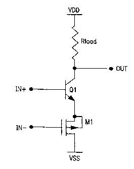
Figure 1 is a simplifi~l 5~ ;c diagram of a charge sensitive amplifier in accoldal1ce with
one embodiment of the present invention.
Figure 2 is a simplified sçl~ ic diagram of an alternative embodiment of the charge
sensitive amplifier of Figure 1.
Figure 3 is a ~;mplified s~h~m~tic diagram of a charge sensltive ~mp1ifi~r in accordance with
15 another embodiment ofthe present i~ve~llion.
Figure 4 is a simplified sf h~m~fic diagram of an alternative embodiment of the charge
sensilive ~mrlifier of Figure 3.
Figure ~ is a detailed sf~h~m~tic diagram of an amplifier CO~ i,l;ilg the charge sensitive
amplifier circuit of Pigure 1.
DETAILED DESCl~IPTION OF TIIE FIGURES
Referring to Figure 1, a charge sensitive ~mplifi-or with high CCillllllOII mode signal rejection
in accordance with one embodiment of the present invention in~ an NPN bipolar jllnr,tion

CA 02244720 1998-07-28
W O98/24176 . - PCTAUS97/20872
l-~nsi~lor ~BJT) Q1, a P-channel metal oxide semiconductor field ef~ect transistor ~P-MOSFET)
Ml and a load reeict~nce Rload, hllelconlle~;Led in a totem pole circuit configuration as shown.
This di~le"lial amplifier confi~-ration has its "positive,l' i.e., noninverting, input terminal at the
base oftransistor Ql and its "negative," i.e., inve~ting, input at the gate of Ll~n~i~lol Ml. Using
5 a BJT at the nol~..vG, lhlg input advantageously ~ul~ ules a shot noise generator in the emitter
current of a BJI for the noise voltage generator a~oci~ted with a MOSFET gate. (It should be
noted that the charge sensitive amplifier with high common mode signal rejection is typically
followed by an inverting gain stage which would, in most applications, reside within the feedbarl~
loop. Hence, the lli,lvt;,li.l~" and llnoninvertingll ~esign~tions are used herein based upon the
10 assumption that such inverting gain stage is present.)
The base ~G"nillal of l.a"~i~lor Q1 receives the noninverting input signal ~N+, while the gate
of transistor Ml receives the inverting input signal IN-. When used in an im~ing system, the
noninverting input signal, IN+ is a positive reference voltage, while the inverting input signal IN-
is the input signal from a selected column of pixel elem~nt~ within the sensor array. With the15 it;~i~Live load Rload at the collector oftransistor Ql, the output signal OUT is an ampli
fied signal
with high conll.,on mode input signal rejection. This high common mode input signal rejection is
realized due to the subst~nti~lly equal signal gains from the inputs IN~, IN- to the output Ol~.
The ~ulJ~L~lially equal signal gains A+, A- from the inputs rN+, IN- to the output Oll'r can
be seen based upon the following analysis. From the illVel Lillg input IN- to the output OUT the
20 signal gain A- is the product of the gain from the ill~/t;l Lilg input IN- to the emitter of transistor Ql
ml11tirlied by the gain from the emitter of ~ .slor Q1 to the output OUT. Hence, the inverting
input signal gain A- is the gain (l,~nscol-lh~ n~e) g",Ml of transistor Ml as a source follower, with
the L~ co~ ct~nce of Lr~ls;;~Lor Ql as its load, multiplied by the gain (transcon~-lct~nce) gmQl

CA 02244720 1998-07-28
WO98/24176 . - PCT~US97/20872
ofthe common base amplifier formed by transistor Ql and the load l e C:~L~ e Rload. This can be
A~ = gm 1 + gQml gm RLO~.D)
;ssed as follows:
A gn~ ,1 ~ RLC~D
gm 1 + gm ¦
With respect to the nonillv~ g input signal IN+, the input stage is transistor Ql as a
commnn emitter ~mrlifi~r with its emitter degeneration equal to the ~ n.scon~uc~nre of ll ansi~o
A ~ RLOAD
gm 1
Ml. Accordingly, the non;ll~rwling input signal gain A+ can be e~.c~sed as follows:
A ~ gm 1 ~ gm 1 ~ R~QAD
gm 1 + gm 1
Based upon the roregoillg, it can be seen that, at least to a first order apploxi~ ;on~ the
inverting A- and noni--~elling A+ input signal gains are sub~lS.nli~lly equal. While this analysis is
10 a~pru~;n~le in the sense that a number ûf higher order effects have not been con~ red (such as
--rB

CA 02244720 l998-07-28
W O98/24176 . PCTr~S97/20872
_ _
back gate m~ tinn in ~ or Ml), circuit ~im~ tions using models for a 0.8 micron BiCMOS
process demonstrate gain m~t~hing to within 0.5%, i.e., 46dB of common mode signal rejection.
In addition to the high colnmon mode signal rejection provided, the circuit of Figure 1 also
exhibits large rejection of noise received via its power supply terminals VDD, VSS. Such rejection
5 is due to the fact that the impedances looking into the ampl;fier from power supply terminals VDD
and VSS <i.e., the load ,e, ~ ce Rload in series with the collector impedance oftransistor Ql, and
the drain i.~ cdal~ce of transistor Ml, respectively) is very high, thereby effectively i.~ol~ting the
input termmals IN+, IN- from mo~ ting signals, e.g., noise on the power supply terminals VDD,
VSS.
One characteristic ofthis circuit which, depending upon the particular application, may be
viewed as a disadvantage is the relatively large input offset voltage (appl~x;.~A~e~y 1.5 volts)
n.qcçss~ry bc;~weell the two input terminals IN~ . However, for many applications involving
charge sensitive ~mplifiers such as this, the nonînverting input signal lN+ is typically a DC r~e t nc~
voltage. Hence, such an input offset voltage requirement is not a problem.
Referring to Figure 2, an ~lt~rn~tive embodiment ofthe charge sensitive amplifier of Figure
1 uses a PNP BJI for transistor Ql and an N-channel MOSFET for transistor M1, with their
respective interconnection~ reversed accordingly. While exhibiting s~,lanLially the same
advantages as the charge sensitive amplifier of Figure 1, this embodiment does have one
disadvantage in that using an N-MOSFET as the signal input device results in a higher level of l/f
20 noise.
Referring to Figure 3, an alternative embodiment of a charge sensitive ~mplifiF~r in
accordance with the present invention uses NPN BlT Q1 and N-MOS~ET Ml in an opposing
circuit confi~-ration biased with a current source ISS and providing a di~t;l,~ial output signal

CA 02244720 1998-07-28
W O98/24176 - PCTrUS97t20872
OUT. While this embodiment exhibits sl~bst~nti~lly the same advantages as the charge sensitive
amptifier of Figure 1, one disa-lv~,l~,e is higher l/f noise due to the use of an N-MOS~ET as the
signal input device.
Referring to Figure 4, an ~ e embodiment of the charge sensitive amplifier of Figure
5 3 uses PNP BJT Ql and P-MOSFET Ml in an opposing circuit configuration biased with a current
source IDD and providing a ~ rel~..Lial output signal OUT. While this embodiment also exhibits
s~;,~ lly the same advantages as the charge se,.silivG amplifier of Figure 1, one disadvantage
is lower gain due to the use of a PNP BJI .
l~eferring to Figure 5, an amplifier circuit co~ .;..g a charge sensitive amplifier in
10 accordance with the present invention, spe~ific~lly the circuit of Figure 1, has NPN BJT Ql and
P-MOS~T Ml coupled between positive VDD and negative VSS power supply terminals. The
load resistance at the collector of transistor Ql is implemented in the form of resistive circuit
provided by P-MOSFET M4 and ~PN BJTs Q4 and Q5. The drain terminal of transistorMl is coupled to the negative power supply terminal VSS via the channel of P-MOSFET M10.
15 As noted above, the noninverting input AINB is a DC~ ~ere,e,lce voltage of app~ 1y 2.5 volts,
while the inverting input signal AIN is a data signal centered about a DC level of app,ox,~,-alely 1
volt.
Based upon the fcrGgoi"g, it can be seen that a charge sensitive ~mplifi~r in accordance
with the present invention has a number of advantages when used in charged integrating amplifier:
20 dirrelel lial input; low input referred thermal and l/f noise; high power supply reiection ratio; high
common mode rejection ratio; and a high impedance input terminal.
Various other mt~rlific~tions and alterations in the structure and method of operation of this
invention will be a~p&lGIl~ to those skilled in the art without departing from the scope and spirit of
!-rB

CA 02244720 1998-07-28
WO 98/24176 . - PCT~US97/20872
the invention. Although the invention has been described in connection with specific plGrellGd
embo-lim~nt~, it should be understood that the invention as claimed should not be unduly limited
to such specific embo~imRnte It is intRn(led that the following claims define the scope of the
present invention and that ~lu~;lules and me~hC~1e within the scope of these claims and their
S e~luiY~lc~ be covered thereby.

Representative Drawing
A single figure which represents the drawing illustrating the invention.
Administrative Status

2024-08-01:As part of the Next Generation Patents (NGP) transition, the Canadian Patents Database (CPD) now contains a more detailed Event History, which replicates the Event Log of our new back-office solution.

Please note that "Inactive:" events refers to events no longer in use in our new back-office solution.

For a clearer understanding of the status of the application/patent presented on this page, the site Disclaimer , as well as the definitions for Patent , Event History , Maintenance Fee  and Payment History  should be consulted.

Event History

Description Date
Time Limit for Reversal Expired 2006-11-14
Inactive: IPC from MCD 2006-03-12
Letter Sent 2005-11-14
Grant by Issuance 2002-01-22
Inactive: Cover page published 2002-01-21
Inactive: Final fee received 2001-10-09
Pre-grant 2001-10-09
Notice of Allowance is Issued 2001-04-25
Letter Sent 2001-04-25
Notice of Allowance is Issued 2001-04-25
Inactive: Approved for allowance (AFA) 2001-04-12
Amendment Received - Voluntary Amendment 2001-03-07
Inactive: S.30(2) Rules - Examiner requisition 2000-11-07
Letter Sent 1999-08-03
Inactive: Multiple transfers 1999-06-16
Inactive: Single transfer 1999-02-17
Inactive: IPC assigned 1998-10-28
Classification Modified 1998-10-28
Inactive: IPC assigned 1998-10-28
Inactive: First IPC assigned 1998-10-28
Inactive: Courtesy letter - Evidence 1998-10-13
Inactive: Acknowledgment of national entry - RFE 1998-10-06
Inactive: Inventor deleted 1998-10-05
Application Received - PCT 1998-10-02
All Requirements for Examination Determined Compliant 1998-07-28
Request for Examination Requirements Determined Compliant 1998-07-28
Application Published (Open to Public Inspection) 1998-06-04

Abandonment History

There is no abandonment history.

Maintenance Fee

The last payment was received on 2001-11-09

Note : If the full payment has not been received on or before the date indicated, a further fee may be required which may be one of the following

  • the reinstatement fee;
  • the late payment fee; or
  • additional fee to reverse deemed expiry.

Patent fees are adjusted on the 1st of January every year. The amounts above are the current amounts if received by December 31 of the current year.
Please refer to the CIPO Patent Fees web page to see all current fee amounts.

Owners on Record

Note: Records showing the ownership history in alphabetical order.

Current Owners on Record
VARIAN MEDICAL SYSTEMS, INC.
Past Owners on Record
MARTIN MALLINSON
MAX J. ALLEN
RICHARD E. COLBETH
Past Owners that do not appear in the "Owners on Record" listing will appear in other documentation within the application.
Documents

To view selected files, please enter reCAPTCHA code :


To view images, click a link in the Document Description column. To download the documents, select one or more checkboxes in the first column and then click the "Download Selected in PDF format (Zip Archive)" or the "Download Selected as Single PDF" button.

List of published and non-published patent-specific documents on the CPD .

If you have any difficulty accessing content, you can call the Client Service Centre at 1-866-997-1936 or send them an e-mail at CIPO Client Service Centre.


Document
Description 
Date
(yyyy-mm-dd) 
Number of pages   Size of Image (KB) 
Abstract 1998-07-27 1 55
Description 1998-07-27 9 351
Claims 1998-07-27 12 439
Drawings 1998-07-27 3 40
Claims 2001-03-06 7 507
Representative drawing 1998-10-28 1 2
Representative drawing 2001-12-19 1 3
Notice of National Entry 1998-10-05 1 201
Courtesy - Certificate of registration (related document(s)) 1999-03-30 1 117
Reminder of maintenance fee due 1999-07-13 1 112
Commissioner's Notice - Application Found Allowable 2001-04-24 1 164
Maintenance Fee Notice 2006-01-08 1 172
PCT 1998-07-27 4 121
Correspondence 1998-10-12 1 31
Fees 2001-11-08 1 42
Fees 2000-10-25 1 37
Correspondence 2001-10-08 1 43
Fees 1999-11-14 1 37