Note: Descriptions are shown in the official language in which they were submitted.
CA 0224~716 1998-08-07
W O 97/31436 PCT/GB97/00520
DARK PULSE TDMA OP~I~AL NETWORK
The present invention relates to an optical network for carrying TDMA
tTime Division Multiple Access) signals and to transmitters and receivers for use in
5 nodes of such a network.
A network embodying the present invention might be used, for example,
as a tocal area network (LAN) for interconnecting computer systems. The
increasing power of computer systems in terms of processor speeds and storage
capacity has made it possibie for conventionai personal computers to handle
10 multimedia applications involving real time video and animation and computer
graphics. The high bandwidth data associated with such applications place heavy
demands on the network and the performance of conventional LANs has failed to
keep pace.
An optical network using synchronous TDMA potentially offers a far
15 higher bandwidth, and so might be used as a high speed LAN to replace a
conventional LAN. However, in existing optical networks, while signal
transmission has been carried out in the optical domain, in practice some electronic
circuits have been required for such functions as channel selection. It has beenrecognised that such electronic components of the network infrastructure
20 constitute a bottleneck restricting the performance of the network.
"A High Speed Broadcast and Select TDMA network Using All-Optical
Demultiplexing", L P Barry et al, ECOC '95 pp 437-440, describes an experimentalOTDM network. At the receivers in the network nodes, an optical clock signal is
detected and a variable delay applied in the electrical domain to the detected clock
25 signal to select a particular TDMA channel. After pulse shaping, the signal is taken
back into the optical domain by driving a local optical source, a DFB laser, which
produces an optical signal for use in a subsequent all-optical switching stage.
The paper by Prucnal et al, "Ultrafast all-optical synchronous multiplex
access fibre networks", IEEE Journal on Selected Areas in Communications, SAC-
30 4, no. g, December 1986 proposes an alternative approach in which differentdelays, and hence different TDMA channels, are selected in the optical domain.
The opticai signal is split between different paths each having a different
CA 0224~716 1998-08-07
W O g7/31436 PCT/GB97/00~20
characteristic delay and an eiectro-optic gate in each path is controlled so that the
signal passes only through the path having the desired delay.
According to a first aspect of the present invention, there is provided an
optical network comprising:
al an optical transmission medium; and
b) a plurality of nodes connected to the optical transmission medium,
each of the plurality of node including a respective dark pulse generator
which is coupled in-line with the optical transmission medium and in series
with the others of the dark pulse generators and which is arranged to
generate dark pulses in an optical signal carried on the transmission
medium .
In this specification, a "dark pulse" is a temporal gap, or region of reduced
intensity radiation, in an essentially continuous burst of optical radiation, or light
beam. An advantage of using dark pulses in place of bright pulses is that optical
1~ signal generation is simplified, as will be discussed in the subsequent description.
Also, while pulse alignment remains important for dark pulse OTDM, to minimise
cross-talk, the extinction ratio necessary for successful dark pulse OTDM
transmission is typically smaller than that required for bright pulse OTDM.
Preferably each node further comprises a variable delay stage which is
arranged to apply a variable delay to a network clock signal in the electrical domain
and which is connected at its output to the dark pulse generator.
The inventors have found it to be particularly advantageous to use in
combination dark pulse generation and channel selection in the electrical domain.
This further simplifies node structures, whilst enabling effective operation at high
2~ bit rates, for example at 40 Gbit/s.
Preferably each node further comprises a clock receiver for receiving a
network clock signal carried on the optical transmission medium, the clock receiver
including a photoelectric detector for converting the clock signal to the electrical
domain.
Preferably the electro-optic modulator is an electro-absorption modulator
(EAMl .
The present inventors have found that significant advantages can be
achieved by combining channel selection in the electrical domain with the use of
CA 0224~716 1998-08-07
W 097131436 PCT/GB97/00520
an electro-optic switch with a fast non-linearity to read the selected channel. In
particular, relatively high switching rates can be achieved without the power losses
typicaily associated with all-optical channel selection. It is found to be particularly
advantageous to use an EAM. The fast response time of such a device makes
5 possible a switching window as short as a few picoseconds. The receiver as a
whole is therefore capable of operating at bit rates of 40Gbit/s or higher.
Preferably the receiver includes means for separating the clock signal in
the optical domain from the received TDMA datastream. Preferably the said
means for separating comprise a polarising beam splitter, in use the clock signal
10 being marked by a different polarisation state to the TDMA datastream.
Preferably a first output of the means for separating is connected to the
optical input of the electro-optic modulator, in use TDMA data passing from the
first output to the modulator, and a second output of the means for separating is
connected to the detector, in use optical clock signals passing from the second
15 output to the detector.
Preferably an impulse generator is connected between the output of the
variable delay stage and the control input of the electro-optic modulator.
The electro-optic modulator may require a drive signal having somewhat
shorter pulses than those output by the delay stage. In this case advantageously20 some form of pulse shaping may be used, and in particular the output of the delay
stage may be applied to an electrical impulse generator. This may be a device
using step recovery diodes to generate short electrical pulses from a sine wave.Preferably the variable delay stage comprises a plurality of logic gates,
means connecting a first input of each gate to an input path for the clock signal,
.~5 control means connected to a second input of each gate, and means connectingoutputs of the gates in common to an output path for the delayed clock signal, the
said means connecting inputs and outputs of the gates to respective input and
output paths being arranged to provide paths of different respective lengths via~ different gates, in use the control means applying control signals to the gates to
33 select a path and a corresponding delay for the clock signal.
This preferred feature of the present invention uses an array of logic gates
to provide an electronic channel selector suitable for an integrated construction,
and capable of quick reconfiguration. This channel selector is not limited in
CA 0224~716 1998-08-07
W O 97/31436 PCT/GB9710052~
applicability to receivers in accordance with the first aspect of the present
invention, but may be used with other receiver designs, or in node transmitters. In
particular, it may be combined with a local optical source in a receiver in which an
all-optical switch was used in place of the electro-optic modulator of the first5 aspect of the invention.
Preferably at least one of the said means connecting inputs and outputs
comprises a microstrip delay line. Preferably the means connecting inputs and
outputs comprise a pair of microstrip delay lines and the gates are connected
between the pair of microstrip delay lines.
Preferably adjacent connections to the gates on the microstrip delay line
on the input side of the gates are separated by a path length corresponding to t/2
and adjacent connections on the microstrip delay line on the output side of the
gates are separated by a path length corresponding to t/2, in use the gates being
controlled to vary the delay by multiples of t, where t corresponds to the channel
spacing in the time domain of the TDMA signal.
Preferably the optical transmission medium is an optical bus, and more
preferably hs an optical bus topology.
As set out in further detail in the description of the embodiments below,
the use of dark pulse generation is found to be particulariy well-adapted to a
network using a bus-topology. This allows the dark pulse generators in the
different nodes to be effectively coupled in series so as to build up an OTDM
multiplex. At the same time, the bus topology eliminates many of the timing
problems associated with other topologies, such as star networks.
According to a second aspect of the present invention there is provided a
method of operating an optical network including a plurality of nodes connected to
an optical transmission medium, the method comprising:
a) at one of the plurality of nodes, imposing dark pulses representing a
data stream on an optical signal which is carried on the optical transmission
medium; and
b) at a subsequent node, receiving the opticai signal including the dark
pulses imposed in step (a~ and imposing dark pulses on the optical signal in a
different respective time slot, thereby creating an OTDM ~optical time division
multiplexed) signal.
CA 0224~716 1998-08-07
'WO 97/31436 PCT/GB97/0052
~he present invention also encompasses an opticai network incorporating
a receiver in accordance with the preceding aspects and also LANs and other
~ computer networks formed using such a network.
Systems embodying the present invention will now be described in further
~ 5 detail, by way of example only, with reference to the accompanying drawings in
which:-
Figure 1 is a schematic of an optical network;
Figure 2 is a diagram showing the structure of one of the nodes of Figure
l;
Figure 3 is a schematic of a transmitter for use in the network of Figure 1;
Figure 4 is a schematic of a receiver for use in the network of Figure 1;
Figure 5 is a circuit diagram for an electrical channel selector;
Figure 6 is a diagram illustrating the use of the electrical channel seiector
with a local optical source;
Figure 7 is a detailed schematic of a receiver based on the topoiogy of
Figure 6;
Figure 8 is a schematic of a pulse source
Figure 9 illustrates a dark pulse generator incorporating one EAM;
Figure 10 is a graph representing a typical operational characteristic of an
EAM;
Figure 11 is a representation of an optical output signal provided by the
system in Figure 9;
Figure 12 illustrates a system incorporating three EAMs; and
Figure 13 is an eye diagram of an optical output signal provided by the
system in Figure 12;
Figure 14 is a schematic of an optical fibre LAN incorporating dark pulse
generators; and
Figures 1 5a and 1 5b show fibre waveguides for use in the ~AN of Figure
14.
An optical network comprises a number of nodes N 1, N2, N3
connected to an optical fibre bus 1. In the present example, the network is a local
area network (LAN) and a number of personal computers PC1, PC2, PC3
are connected via the optical fibre bus to each other and to a network server 2.
CA 0224~716 1998-08-07
W O 97/31436 PCT/GB97/O~S20
Although, for clarity, only three nodes are shown, in practice the network may
support many more nodes. The network uses a structure termed by the inventors
a re-entrant bus topology. As seen in Figure 2, each node includes a transmitter21 coupled to the bus 1 at two points and a receiver 22 coupled to the fibre bus 1
5 at a point downstream from the transmitter. The transmitter 21 and receiver 22are coupled to the respective personal computer by an electronic interface 23.
The network operates using a synchronous TDMA (time division multiple
access) protocol. A clock stream is distributed to all users of the network thereby
ensuring that each node is synchronised. A clock pulse marks the start of each
10 frame. The frame is precisely divided into time-slots - for example slots of 10ps
duration for a 100Gbit/s line rate. In general each node has a tuneable transmitter
and tuneable receiver and can thereby transmit and receive in any of the time-
slots. The granularity of the network, that is the relationship between the overall
network bandwidth, and the bandwidth of individual channels, may be chosen to
15 be relatively high so that each user has access to a relatively low speed ~say
155Mbit/s) channel from a fibre optic pipe which itself carries rates in excess of
100Gbit/s. To minimise the costs of the electronic components required, the
electronic speeds within each node are at most 2.5Gbit/s in this example. The
clock source is typically located at the network controller 3 associated with the
20 server 2. The clock produces a regular stream of picosecond duration optical
pulses at a low repetition rate, say 155 or 250MHz, relative to the peak line rate of
the optical pipe (100Gbit/s) . Such a source may be provided by a mode-locked
laser or a gain-switched laser with external pulse compression. As a guideline, for
a 100Gbit/s LAN a pulse duration of around 2ps is required whereas for a 40Gbit/s
25 system around 5-7ps suffices. A pulse source suitable for operation at 100Gbit/s
or higher is disclosed and claimed in the present applicant's co-pending European
Patent Application filed 16th February 1996 and entitled "Optical Pulse Source"
~applicant's ref. A25146). The disclosures of that earlier application are
incorporated herein by reference. This pulse source may comprise a ridge-
30 waveguide gain-switched distributed feedback semiconductor laser diode ~DFB-
SLD) having its output gated by an electro-absorption modulator. Continuous
wave (cw) light is injected into the optical cavity of the D~B-SLD. A synchronised
CA 0224~716 1998-08-07
W O 97/31~36 PCT/GB97/00520
RF drive is applied to the DFB-SLD and to the EAM. This pulse source is shown
schematically in Figure 8.
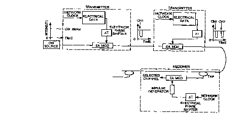
Figure 3 shows the transmitter in one of the nodes. At the transmitter, a
fraction of the distributed clock stream is split-off and then encoded via an electro-
5 optic modulator. This may be, for example, a lithium niobate modulator such asthat available commercially from ~Jnited Technologies, model no. APE MZM-1.5-3-
T-1-1-B/C, or an electro-absorption modulator (EAM). A suitable EAM is describedin the paper by D.G. Moodie et al published at pp 1370-1371 Electron. Letts., 3
August 1995, Vol 31, no. 16. The variable time delay in the transmitter then
10 places the modulated pulse stream into the correct time slot for onward
transmission. The data and clock streams must be distinguishable, and in this
example poiarisation is used to distinguish the clock from the rest of the frame. In
the transmitter, a polariser P eiiminates the possibility of data channels breaking
through and being modulated in the electro-optic modulator (EOmod). The polariser
15 need not be a separate device but might be integrated with the EO modulator. For
example, the United Technologies EAM referred to above is inherently polarisation-
selective in operation . The delay line provides the required delay and data pulses
are inserted into the appropriate time-slot with a polarisation orthogonal to the
clock stream. This polarisation rotation may be done via a simple polarisation
.~0 rotator such as a retardation plate or, where polarisation maintaining fibre is used
to implement the circuit, then rotation may be achieved by physically rotating the
waveguide before reinserting it into the fibre optic pipe.
At the receiver, after tapping a fraction of the light from the optical pipe,
the clock and the data are separated. A polarising beam splitter (PBS) is used to
.~5 perform this function. The clock and the data pulses are then forced to suffer a
relative (programmable) optical delay using a variable time delay device. This
means that the clock pulse can be temporally overlapped with any data pulse slotand therefore used to demultiplex or read any channel. After the channel is
~ demultiplexed, it is converted back into the electrical domain using a receiver
30 operating at up to 2.5 Gbit/s, the allocated bandwidth per user.
Figure 4 shows in detail the structure of the receiver and in particular
shows how an electrical channel selector (ECS) is used to provide a signal which,
after suitable amplification and shaping drives an electro-absorption modulator
CA 0224~716 1998-08-07
W O 97/31436 PCTIGB97/OOS20
(EAM). The electrical channel selector (ECS) is shown in Figure 5. The optical
LAN clock is first detected using a detector 52 which might be, for example, a PIN
photodiode. After amplification, the signal is filtered to generate a clean electrical
sine wave. The signal is then input to a delay stages 53 comprising a series of
5 electrical AND gates LG arranged in a linear array. The array is implemented as a
single low cost chip available commercially as NEL NLB6202. The AND gates
control access to the microstrip delay lines. The delay lines are accurately stepped
in delays equal to the channel separation of the LAN. For a system operating at
40Gbit/s, the channel delay t equals 25ps. The AND gates are controlled via an
10 input from a demultiplexer 54. In this example the demultiplexer is an NL4705device manufactured by NEL. ~he demultiplexer converts an incoming serial delay
select word generated by the PC connected to the node into an appropriate gatingsignal for the ANO gate array and thereby selects the appropriate delay.
The electrical channel selector produces at its output a stepped sine wave.
15 This may then be amplified and suitably shaped in order to generate the
appropriate drive signal required for the next stage. The next stage may be, forexample, an EAM, or a laser diode. If the pulses output by the ECS require
shortening to drive the next component, then an electrical impulse generator maybe used. A suitable coaxial step recovery diode comb generator is available
20 commercially as ELISRA series MW15900. Given that electronic clock recovery
can be carried out with sub-picosecond temporal jitter and microstrip delay lines
can be controlled to picosecond accuracy, it is potentially possible to use such an
electrical channel selector at rates as high as 1 00Gbit/s.
Although the circuit of Figure 4 uses an EAM, the ECS might alternatively
2~ be used in combination with a local optical source. With such a source, the ECS
may be used either in the transmitter for programmable channel insertion (Figure6), or in the receiver for channel dropping (Figure 7). In the case of channel
dropping, the output of the local picosecond pulse laser is combined with the data
in an optical AND gate. Advances in picosecond pulse lasers in recent years are
30 such that it is possible to generate stable picosecond duration optical pulses using
semiconductor based active media. One example of such a laser is a gain-
switched DFB laser followed by chirp compensation as described in our above-cited
copending application. This provides a simple reliable source of picosecond
duration pulses at flexible repetition rates from Ml Iz to 10s of GHz. In the present
CA 0224~716 1998-08-07
W O 97/31436 PCT/GB97/00520
example, such a source is driven by the output of the ECS after broadband
amplification and using an impuise generator. The resulting stream of optical
pulses is then used directly to demultiplex the required channel in an optical AND
gate. The use of an optical AND gate as a demultiplexer is described in detail in
5 the present Applicant's earlier International Application no. PCT/GB 95t00425,filed 28th February 1995. The wavelength of the source depends on the design
of the optical AND gate, but is not at all restricted to be the same as the datawavelength. The optical AND gate may be an SLA - NOLM or may be an
integrated semiconductor-based device.
The systems so far described have used what may be termed "bright
pulses" to carry information. Advantageously, dark pulses may be used instead. Aconvenient system for generating dark pulses will now be described. Initially the
description covers the case of a system incorporating only one EAM. Typically,
however, more than one EAM would be utilised, as described in more detail below.In Figure 9, a 1555nm DFB laser source 110 is coupled into an EAM 120
with a power level of -2dBm. The EAM has a maximum extinction ratio of 20dB
and a mean absorption characteristic of 2.5dB/V. A 10 GHz sinewave drive 142 is
synchronised with and passively added to a 10Gbit/s data sequence from a data
source 144 via a power splitter 140 (used in reverse to combine the two signals).
20 A suitable power splitter is the Wiltron K240B, available from Anritsu Wiltron.
Both the sinewave and data sequence signal levels have a 2.5V peak-to-peak
amplitude. The resulting signal comprises a sinewave with an offset voltage
determined by the data signal, with the relative amplitudes arranged such that the
maximum value of the cycle for a data O is below the minimum level for a data 1.25 It will be appreciated that this precise arrangement is not necessary, and it would
be sufficient to ensure that the entire 10 GHz cycle remains in the low absorption
region of the modulator for a data 1. The electrical signal is applied to the EAM
120, and the DC bias is adjusted to ensure that the entire cycle for a data 1 gives
low extinction, whilst the troughs of the cycle for a data O give a high extinction.
30 Consequently, dark-pulses are formed for data O's, whilst a low extinction is maintained for data 1's.
An EAM suitable for use in the system is the one described in, for
example, "Generation of 6.3 ps optical pulses at a 10 GHz repetition rate using a
CA 0224~716 1998-08-07
W O 97/31436 PCT/GB97/00520
packaged EAM and dispersion compensating fibre", Electronics Letters, Volume
30, pp 1700-1701, which is incorporated herein by reference. The absorption
characteristic of this EAM is reproduced in Figure 10. In Figure 10 it can be seen
that the EAM has an operating region of low extinction at positive or low negative
reverse biases, an operating region of high extinction at high reverse biases, and
an exponentially varying operating region in between. It is the exponentialiy
varying operating region of the EAM which supports the generation of soliton-like
dark pulses.
In theory, the dark pulses generated should resemble inverted SECH2
10 pulses (that is to say, inverted solitons) having the form:
P(t) = ~Peak Power) x (1 - SECH(1.76(t/l~)2) (equation 1)
where I represents the pulse width at half its peak power. In operation, the EAM15 is electrically biased to remain in its low loss condition unless both data and
sinewave are negative. That is to say, the EAM transmits light unless both
electricai signal components are negative. Thus, dark pulses are generated
corresponding to data zeros, as illustrated in Figure 11, which closely resemble the
theoretical form of equation 1.
Figure 12 shows a system according to the present invention
implementing three EAMs. In the system, three EAMs 400, 410 and 420 are
optically cascaded, or are arranged to be in optically coupled alignment, with an
optical light source 100, comprising a 1555nm DFB laser. Conveniently, the laserlight is coupled onto the first EAM 400, using a standard telecommunications
25 optical fibre 105, the light having a power level of -2dBm. In this example, optical
amplifiers 405,415 and 425, for example EDFAs, follow each EAM to compensate
for any losses incurred in the EAMs. The amplifiers are only incorporated if
necessary to compensate for optical loss incurred by the EAMs. As for the systemillustrated in Figure 9, each EAM is driven by an electrical signal comprising a30 sinewave component and a data component aligned in data channel slots A, B orC. Since three electrical drive signals are required, electrical timing circuitry 450 is
required to ensure that the data signals A, B and C are aligned correctly with the
CA 0224~716 1998-08-07
W O 97/31436 PCT/GB97/00520 1 1
sinewave and are aligned also in the correct slot positions of the required OTDMsignal which is output downstream of the third amplifier 425.
The light source can be separate from the modulator, the light from the
light source being coupled into the modulator via, for example, an optical fibre as
5 described above. However, in an alternative arrangement the light source and the
EAMs are fabricated as an integrated device on a common semiconductor
substrate. Apart from convenience, this arrangement has the advantage that
coupling loss between each modulator and between the light source and the first
modulator is reduced. Also, amplification, if necessary, could be provided by
10 integrating SLAs (semiconductor laser amplifiers) between one or more EAMs.
The skilled person will appreciate that any form of optical, acousto-optic or
electro-optic modulator having the necessary transmission and extinction or
switching properties to provide dark pulses would be suitable for implementing the
present invention.
The electrical bias scheme described above for driving the EAM is
particularly advantageous for two reasons. Firstly, only one electrical signal is
required to bias each EAM and secondly the electrical signal does not require any
electrical processing. Electrical processing would be required if using the method
described in "Generation of 2.5Gbit/s soliton data stream with an integrated laser
20 modulatortransmitter", Electronics Letters, Volume 30, pp 1880-1881.
EAMs suffer some optical loss even when operating in their low optical
loss regions. The amount of optical loss of an EAM is partly determined by the
length of the optical modulator section through which light from a light source
travels. Thus, in known modulator schemes comprising two modulators or multiple
25 modulator sections, which firstly generate an optical pulse stream using an
electrical sinewave drive signal, and secondly modulate data onto the pulse stream
using an electrical data signal, both modulators, or both modulator sections, incur
an optical insertion loss. In that the proposed system only implements one
modulator (section) per data channel, the system intrinsically incurs a lower
30 insertion loss overhead, regardless of the type of modulator used, than otherschemes incorporating more than one modulator, or modulator section, to generateone data channel.
CA 0224~716 1998-08-07
W O 97/31436 12 PCT/GB97/00520
As described above, the optical radiation is in the form of a substantially
continuous burst. The duration of the burst depends on the application. For the
example of a trunk communications network, where traffic is iikely to be present at
most times, the optical source might remain on all the time. Alternatively, for a
less busy optical link, the source might be switched on only when transmission of
data, or part thereof (for a packet switched network for example), is required.
Therefore, 'substantially continuous' might be interpreted as continuous during
data transmission.
Alternatively, the cw light input into the first EAM can be substituted for
an optical clock, for example a sinewave or pulse stream. Then, with the same
general system arrangement used for dark pulse generation, each EAM can be
used to modulate one time slot of the optical clock. That is to say, each EAM isarranged either to transmit, or prevent transmission, of light Ithe peaks or bright
pulse portions of the clock signal) depending on the data-encoding requirements of
its designated data channel. For example, for a 1 00Gbit/s optical clock pulse
stream, ten EAMs may be cascaded to encode ten 10Gbit/s channels. Also, one
or more EAMs operating according to this arrangement may be used as data-insert
devices for one or more channels in an OTDM system. The skilled person would
easily be able to implement data modulation or an insert function by applying the
theory disclosed by the present description.
The skilled person will also appreciate that the level-shifted sinewave bias
signal described above for generating dark pulses would be suitable for generating
bright pulses when applied to a single electrical input EAM. The electrical signal
would in this case need to be arranged to maintain the EAM in its high optical
extinction state unless both data and sinewave components were positive. Such
an arrangement would obviate the need for electrical signal processing to generate
a suitable bias signal, and would thus be a simple and robust solution. Thus, this
arrangement could be used for generation of solitons or a conventional OTDM
signal .
Figure 14 shows dark pulse generators incorporated in a network using the
re-entrant bus topology described previously. It differs from the networks
considered previously, in that the time-slot into which data is added at a node
transmitter can be chosen in the electrical domain. Each node transmitter has a
CA 0224~7l6 1998-08-07
W O 97/31436 13 PCT/GB97/00520
respective EAM connected in-line with the optical fibre and with the EAM's of
other node transmi~ters. By contrast, in the receivers, the EAM's do not need tobe in-line, and preferably are connected to the optical fibre by an optical tap in
order to optimise the power budget. As described above, and in our co-pending
5 European patent application no. 96301277.8 filed 26 Feb 1996, the contents of
which are incorporated herein by reference, the network clock may be distributedalong the optical ~ibre bus using a different polarisation state to distinguish it from
the optical data on the bus. It is preferred however that the bus shouid comprise
two co-located optical fibre waveguides, with one of the two waveguides
10 dedicated to carrying the clock signal, as described in our co-pending European
patent application no. 96304694.1 filed 26 June 1996, also incorporated herein by
reference. As shown in Figure 15a, the two waveguides may be prG)vided by twin
cores 151, 152 within a single optical fibre 153, Alternatively, as shown in Figure
15b, two or more optical fibres 51a-51d may be co-located within a single sheath15 53 using e.g a blown fibre cable construction including aramid yarn reinforcement
~i4. The optical signal for modulation by the EAM of the dark pulse generator isthen transmitted down one of the waveguides while the network clock signal is
transmitted down another of the waveguides. The network clock does not need
necessarily to be a short optical pulse, since in this embodiment the clock is not
20 modulated directly to produce the data channels. A relatively broad optical pulse.
or modulation of a CW beam may be used to generate the clock. The network
clock is converted to the electrical domain and a variable delay applied in order to
generate a control signal for the EAM in the appropriate respective time slot. This
signal is modulated with RZ data received, for example, from a PC data interface25 of the type previously described. I~ the electrical data is originally in an NRZ
format, then conversion to RZ with a low duty cycle is required in order to produce
narrow dark pulses.