Note: Descriptions are shown in the official language in which they were submitted.
CA 02245872 1998-08-06
W O 97/32405 PCT~US97/02348
INTERFERENCE CANCELLATION SYSTEM FO~
GLOBAL POSITIONING SATELLITE RECEIVERS
BACKGROUND OF THE INVENTION
~ 51. Field of the Invention
The present invention relates to a nulling and cancellation system for Global
Positioning System (GPS) receivers adapted to suppress inband interference and/or
denial j~mming signals in the GPS L1 and L2 ~requency bands. More specifically,
the present invention relates to the reception of orthogonally polarized electric field
vectors and to methods of receiving these components with high cross-polarized
isolation, and to the methods of attenuating interference and/or j~mming signalsusing adaptive polarization mismatching of the antenna feed signal received ~y the
victim GPS receiver. The present invention suppresses interference and/or jamming
by signific~ntly reducing the jammer-to-signal (J/S) ratio seen by the GPS receiver.
2. Description of the Prior Art
The Global Positioning System (GPS) [also called NAVSTAR] is a satellite
navigation aiding system which transmits digitally coded data used to determine 2
and 3-dimensional position fixes at a receiving antenna. Its purpose is to provide
users with high accuracy position, velocity and universal time throughout the world
at low cost. For this reason, relia~le GPS operability in an interference
environment is valuable for both military and civilian applications.
The key to achieving precise navigational performance is the processing of a
very weak GPS spread spectrum signal which carries coarse acquisition (C/A) and
precision (P~Y)3 digitally coded and encrypted data, typically -120 dBm to -136 dBm
(isotropic). The GPS signal spectrum uses two L-band frequencies, L1 at 1575.42
MHz and L2 at 1227.60 MHz, with bandwidths of either 2.05 MHz for C/A code or
~0.46 MHz for P(Y) code, and employs right hand circular polarization (R~CP) forboth L1 and L2 to simpli~y user dependence on receive antenna orientation. The
C/A and P(Y~ codes are on L1, the P(Y) code is on L~. Theoretical processing
- gains for the CIA alld P(Y~ codes are 43 dB and 53 dB, respectively. The critical
C~PS receiver reception st~tes are: C/A code acquisition; P code direct acquisition;
P code track; and P code carrier aided track.
CA 02245872 l99X-08-06
WO 97/32405 PCT/US97/02348
The GPS digital data can be detected and processed even if RF carrier
reception is prevented by interference, but higher accuracy is attained when thesignal carrier is available. This is generally possible because the GPS concept has
inherent a~tiJam (AJ) capability, ~owever the low receive signa} level makes GPSvulnerable to low power interference and/or j~Tnming. It is relatively easy for a
loGal inband source to overwhelm the GPS signal, preventing successful processing
of the digital data. As a result, the GPS system has several identified susceptibilities
and vulnerabilities to interference. From both military and civilian perspectives, it is
important to establish an adequate antijam capability for GPS systems and ensureavailability of this asset in al~ environments. This was recognized by the military and
resulted in the development of several spatial nulling and/or beam forming antennas
and di~ital filtering concepts.
C~P~ receivers have exhibited different levels of vulnerability to interference
and j~mming emitter waveform types, including: broadband Gaussian noise,
coIltinuous wave (CW), swept CW, pulsed CW, amplitude modulated (AM~ CW,
phase shift lceying (PSK~ pseudo noise, narrowband and wideband frequency
modulated signals, etc. Vulnerability is highly scenario and receiver mode
dependent. Broadband G~l~sci~n noise is the most critical interference type in the
above group ~ecause of the difficulty in filtering broadband noise without
concurrent ~PS quieting, and the intrinsic high cost and performance impact
associated with spatial filtering, i.e. null steering, solutions on a moving platform.
~he use of phase nulling is generally known in the prior art aIthough the use
of polarization converted to phase for GPS interference nulling applications is not
known.
It is desirable to provide an interference cancelling system for GPS systems
that can deal with comp}ex interference environments composed of diverse
interference and/or j~mming waveforrn types, L1 and/or L2 interference, multipleinterference sources, and ~ifferent interference polarizations. It is further desired
that the interference cancelling system provide high levels of cancellation for either
or ~oth of the GPS opera~ng frequencies and adapt to variation in orientation ofthe receiver antenna(s) and~/or the interference source.
CA 02245872 1998-08-06
W O 97/32405 PCT/US97/02348
SIJMM~RY OF THE INV3~NTION
One object of the present invention is to provide an interference nulling
system for GPS which exploits the differences in apparent polarization of the right
hand circular polarization GPS signals and interference sources, and to suppressS inband interference and J~mming signals in the GPS L1 and 1,2 fre~uency bands.
It is a further object of the present invention is to provide an antenna system
that processes ~e orthogonal elements of the interference signal(s) and of the GPS
signals with a high degree of cross-polarization isolation and to adaptively cross-
polarize the antenna system and null the interference.
Another object of the present invention is to receive the interference signals
using one port of an adaptive antenna feed circuit having an RF polarimeter
structure and to sample the interference signal so as to modulate the combined
interference signals and GPS signals and to null out the interference signal in the
port to the GPS receiver.
Still further, a general object of the present invention is to provide an
orthogonal polarization receive antenna structure having a compact form, a ~ow
profile, and capable of processing the L1 and L2 GPS signals independently.
It is another general object of the present invention to provide a nulling
system capable of cancelling multiple interference sources having a coherent
relationship that allows vector summation, and to cancel multiple interference
sources having similar polarizations.
Yet another general o~ect of the present invention is to detect the
interference signals and control the adaptive cross-polarization nulling system
~thout ~e need to process the GPS signal.
2~ Ano~er general ol~ject of the present invention is to partition the antenna
and adaptive cross-polarization nulling circuits such that the antenna subsystem may
be remotely located and powered, and that the electrical interface between thesefunctio~l elemen~s be composed of a minimum number of RF coaxial or fiber optic
ca~les and wires.
Another general objec~ of the present invention is to utilize multiple
~nplementation configurations and system modularity which address irldividual
reqnirements to process interference in L1 only, L2 only, L1 and L2, Ll with L2
CA 02245872 1998-08-06
W O 97/32405 PCTNS97/02348
bypassed, etc.
It is another general objective of the present invention to present an installedinsertion lossJgain to the GPS receiver that improves GPS receiver performance
range.
According to these and other objects of the present invention, there is
provided a high quality orthogonal polarization receive antenna system that
decomposes the received ~-band environment into the apparent orthogonal
polarization signals representative of the GPS signal and inband interference
sources. T~e orthogonal components of the received environment are filtered,
amplified ~nd transmitted from the antenna system to the nulling system in each
GPS band using separate cables. In the case of the L2 bypass configuration, the
right hand c~rcular polarization signal may be developed at the antenna and
transmitte~. A sample of the interference signal in each band of the GPS channel is
detected and processed to identify interference conditions and to produce control
signals that are applied to the adaptive antenna feed circuits in each band of
interest that control the effective tilt angle and ellipticity (or axial ratio) of the
combined antenna system. The effective polarization property of the antenna
system is controlled so as to cross-polarize or mismatch the antenna to the
interference source and thus null or suppress the interference signal in the channel
containing the GPS sign~l~ In configurations where L1 and L2 bands are processedseparately, they are recombined after independent nulling, and provided to the
victim GPS receiver. T~e detection and control loops are optimized to identify and
acquire interference signals and to rapidly modulate the tilt and ellipticity properties
of the ada;ptiYe system to a null. Adaptation includes variation to polarizationproperties~ polarization orientation, fading, maneuver variations, etc. Under a no
interference condition, each adaptive L1/L2 loop can be configured so that the
effective pola~ization property of the antenna system to the preferred right hand
circular polarization for optimum receipt of the GPS signal using the GPS receiver.
3û BlE~IEF DESC~IPTI[ON OF THE DRAWINGS
Fig. 1 is a top-leYel block diagram showing the adaptive cross-polarization
interference cancellation system for GPS ~ign~
CA 02245872 1998-08-06
W O 97132405 PCT~US97/02348
Figs. 2A-2F show various alternate implementation approaches possible for
the invention based on representative applications for GPS receivers and GPS
accuracy requirements. The Figs. illustrate three categories of implementation: a
single ortho antenna configuration; dual ortho antenna configurations; and dual
antenna ortho bi-frequency antenna system configurations.
Fig. 3 illllstrates one preferred embodiment of a single channel dual ortho
antenna configuration for nulling of L1 (or L2) interference only.
Fig. 4 illustrates a second preferred embodiment utilizing a dual ortho
antenna bi-frequency configuration for nulling of L1 interference and L2 bypass.Fig. 5 illuskates the structure of the ortho bi-frequency patch ar tenna
showing two rectangular microstrip patches (not drawn to scale) in an orthogonalarrangement with independent L1 and L2 orthogonal feeds.
Fig.-6 illustrates the structure of an ortho bi-frequency patch antenna
showing two rectangular mic.o~llip patches (not drawn to scale) in an orthogonalarrangement with fre~uency multiple~ced L1 and L2 orthogonal feeds.
Fig. 7 ~llustrates the methodology for locating the optimum 50Q impedance
feed ports for the ortho bi-frequency rectangular patch antennas for L1 and L2
orthogonal feeds.
Fig. BA i~lustrates the RF block diagram and receiver processing schematic
for one channel or loop of interference cancellation.
Fig. 8I3 il~ustrates an alternative interference receiver detector circuit that
may be utilIzed in the Fig. gA embodiment.
Fig. g illustrates the modulator schematic for the polarimeter or gamma/phi
modulator portion of the ~ vw~ve section of the invention.
Fig. 10 Illustrates the down converter schematic for a superheterodyne
interference receiver/detector circuit.
Fig. 11 illustrates the IF amplifier and video detection schematic for a
superheterodyne interference receiver/detector circuit.
Fig. 12 illustrates a logarithmic ampiifier schematic for the interference
receiver/detector circuit of Fig. 8B.
Fig. 13 illustrates the varactor controlled phase shifters of the polarimeter
modu}ator of Fig 9.
CA 02245872 l99X-08-06
WO !~7/32405 PCT/US97/02348
Figs. 14, 15 and 16 illustrate the GPS interference canceler control algorithm
for detecting and cancelling interference.
DESCRIPTION OF ~3:E PREFERRED EMBODIMENTS
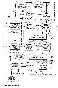
A top-level block diagram showing the adaptive cross-polarization
interference cancellation system for GPS signals is shown in Fig. 1. The diagramillustrates one channel or band of the invention showing the cancellation concept
and illustrating the received signal composed of the combined GPS signals 1 and the
interference or j~mming signal 3. The received signal 1, 3, consisting of the GPS
signals and the interference signals, is received by the antenna system 5 whieh
effectively divides the received signals into orthogonal components VP and HP
{vertically polarized and horizontally polarized) signals to the adaptive antenna feed
system 7. A power coupler 9 samples the difference port 11 of the network which
lprovides the difference signal to the GPS receiver (not shown) via 13. An
interference receiver deteetion eircuit 15 receives and processes the difference signal
and provides the signal to adaptive control eireuits 17 that control the phase
modulators within the adaptive antenna feed system 7 for tilt and ellipticity. The
loop closes on interference to cross-polarize the feed and to null the interference to
the GPS reeeiver. The GPS receiver may, optionally, provide a jam indication
enable signal 19, via a GPS interface 21, to enable or disable the receiver circuit 15.
When enabled, a "~am detection" signal 23 may be provided back to the GPS
reeeiver.
For purposes of explaining the operation of the present invention for nulling
a signal, it is assumed that a]l received signals, GPS signals 1 and interference signal
3, are composed of vertica~l and horizontal polarized waves. The theory supporting
the ortho polarizatio~ nuIling concept used in the invention is based on the property
that any wave of arbitrary polarization can be synthesized or decomposed from/into
two waves orthogona~ly polarized to each other. For example, a circularly polarized
wave can be produced by ~he coexistence of a vertically and a horizontally polarized
wave, each having the same amplitude and with a 90-degree phase difference. A
linearly polarized wave can be produced by the coexistence of a vertically and ahorizontally polarized wave, with a 0-degree phase difference. Thus, orthogonal
- 6 -
CA 02245872 1998-08-06
W O 97~32405 PCTAUS97/02348
polari2ation antennas can be used to match or mismatch a propagated signal usingrelative phase and ampliblde modulations to combine the ortho components. For
the case of an interference signal, the orthogonal polarization antennas within the
antenna system 5 can be used to mismatch the receiving system and effectively null
S the signal. This mismatch null would have an impact on other signals in the
environment, including the desired ~PS signals, by creating conditions in the
antenna tha~ could range from a perfect match to a mismatch as well.
The loss, null or mismatch achievable using polarization mismatch can be a
value between infinity and zero. The theoretical polarization mi~m7teh loss, X, can
lû be calculated for two wide~y separated elliptically polarized antennas in freespace
using the following relationship:
0 1~glO { 1/~ ~ 1/2~4YT1~R + (1 YT )~1 --YRZ)(COS 213)~ }
(1 ~ Y~ )(1 + YR )
where:
y = ellipticity ratio, the signed voltage ratio of the major axis of the
polarization ellipse to its minor axis, (1' IylcOo).
,B = polarization mismatch angle, (0~s,B~90~).
T= transmit; R = receive.
The polarLmeter implementation utilized within the invention effectively
modulates the orthogonal received components of both the interference signals and
the GPS signals and via a detection and closed loop control creates a polarization
mismatch against the interference signal in the signal path to the GPS receiver.2~ Figs. 2A-2F show various alternate implementation approaches possible for
the invention based on representative applications for GPS receivers and GPS
accuracy re~uirements. The Figs. 2A-2F illustrate three categories of antenna and
interface imp~ementations: (a) a single ortho antenna confgz~ration (Fig. 2A) that
can be applied to the Ll or L2 band where a single channel of nulling is
implemented in either Ll or L2 bands; (b) the dual ortho antenna confgurations
~ ~Figs. 2B and 2C~ using a~ implementation where separate L1 and L2 band
antennas process the or~ogonal received signals in each band for L1
-- 7 -
CA 02245872 1998-08-06
W O 97/32405 PCTAUS97/02348
nulling/cancellation and L2 bypass (Fig. 2B), and an implementation where separate
L1 and L~ band antennas process the orthogonal received signals in each band forindividual L1 and L~ nulling (Fig. 2C); and (c) the dua~ antenna ortho bi-frequenc~
~nte~no. syslem configu~tJons (Figs. 2D-2F) using implementations wbere a pair of
bi-frequency antennas furnish the orthogonal electrical components of the L1 andL2 bands having higher cross-po}arization isolation and where the orthogonal
received signals in each band are used for L1 nulling/cancellation and L2 bypass~Fig. 2D), a second implementation where the orthogonal L1 and L2 band signals
are processed in each band for individual L1 and L2 nulling (Fig. 2E), and a third
(minimum interface) implementation where a pair of bi-frequency antennas furnishthe combined sum of the orthogonal components of L1 and L2 bands whereby the
signals are frequency multiplexed in each patch antenna by virtue of the antennafeed position ~Fig. 2F).
Fig. 3 depicts one preferred embodiment of a single channel dual ortho
antenna configuration for nulling of L1-band (or L~-band) interference only. Theantenna system S provides vertically and horizontally polarized signals VP, HP to
the adaptive antenna feed system 7. The antenna system S includes an antenna(s)
2~ which may be either a pair of L1 dipoles oriented for orthogonal operation, or
one L1 mi~lo~ patch antenna with vertical and horizontal ortho feed. Patch
antenna configurations are generally known in the art. Alternatively, the antenna 25
may be the novel bi-frequency antenna of Figs. S and 6 which provide the L1
vertical and horizontal components for each channel. The antennas 25 receive or
detect the L1 (or L2) GPS signals along with any inband interference signals. The
detected vertical and horizontal components pass through band-pass filters 27, 29
and pre-amplifiers 31, 33 to provide the VP and HP .sign~
Illustrated in Fig. 3 is the polarimeter architecture (sometimes referred to as
a gammalphi modulator~ 35 of the feed system 7, whereby the unequal phase ~or
delay) of the received ortho signals VP, HP are first adJusted for tilt (phi) torelative quadrature by ~ariable phase control circuits 37, 39 acted upon by adaptive
phase controller 41 of the adaptive control circuit 17, and then combined in the first
~brid junction 43. The unequal phase (or delay), or phase shift of the received
ortho signals VP, HP resul~ from the relationship of the two received signal
CA 0224~872 1998-08-06
W O 97132405 PCTAUS97/02348
components and by unequal delays in the tr~ncmi~ion lines and networks between
the antennas 25 and the polarimeter 35. The output signals of the first hybrid 43
are theoretically equal in amplitude. The outputs 43a, 43b of the first hybrid 43 are
adjusted in relative phase by variable phase control circuits 45, 47 acted upon by
S adaptive phase controller 49 of the adaptive control circuit 17 and then combined in
the second hybrid 51 to produce a minimum null at the difference output port 53
that is effectively, or desirably, the null of the interference signal. The second
output 5~ of the hybrid ~1 is a sl-mming port 55 and concurrently produces a
maximum output. Balanced varactor phase shifter arrangements, described below,
are used in each leg of the gamma (45, 47) and phi (37, 39) modulation process to
provide matched operation over frequency and power. The difference (or delta)
and summing (or sigma~ outputs 53, 55 of the second hybrid junction 51 are
detected, processed by the interference detection receiver circuit, or receiver
processing c~rcuit, 15, and used to adaptive}y generate loop control signals for tilt
and ellipticity (or g~mm~phi) modulations by adaptive control circuit 17. The
control loop compensates the system for installation variations, apparent
interference signal changes, and for component unbalances. The null or difference
output 53 of the second hybrid 51 is also provided to the GPS receiver, via a power
coupler 9, as an input 13 with the interference signal suppressed.
Fig. 5 shows the structure of a dual ortho bi-frequency patch antenna
showing two rectangular microstrip patches 61, 63 in an orthogonal arrangement.
The dimensions Dl and D2 of the two microstrip patches, 61 and 63 are the same
for each patch and are selected to optimally receive the L1 and L2 bands with
orthogonal ~inear polari~ations, respectively, i.e. Dl approximately equals ~Id/2, D2
appru~lllately equals ~ 2~ where Ald and ~2d are the signal wavelength for L1 and
L2 in the antenna dielectric, Dl is one dimension of each patch, and D2 is the
second orthogonal dimension of each patch, as will be discussed further below. The
patch antennas 61, 63 may be located on a single printed circuit board. Patch
antenna configurations are well known in the art and generally comprise a
conductive portion 65, ~7 overlying an electrically thin dielectric substrate portion
6g, 71 overlying a conduct~ve ground plane 80 with feeds or probes connected with
the conductive portions. In the present inven~ion, the feed or probe locations of the
-
CA 02245872 1998-08-06
WO 97/32405 PCT~US97/02348
patches are selected to provide optimum linear signal coupling and cross-
polarization isolation. In this embodiment, four (4) feed locations 73, 75, 77, 79 are
used to independently provide the L2/V, L1/H, Ll/V and L2/H polarization (P)
electrical ~ign;~
Fig. 6 shows an alternate structure for a dual ortho bi-frequency patch
antenna showing the two rectangular microstrip patches 81, 83 in an orthogonal
arrangement. ~he dimensions and orientation of the two microstrip patches, 81, 83,
are the same as discussed above using a novel feed arrangement selected for
frequency multiplexed operation. The feed or probe locations 85, 87 are located
1() along the diagonals 89, 91, or diagonal regions, of each patch and are selected to
provide optimum combined signal coupling and cross-polarization isolation for L1and L2 signals. Two feed locations 85, 87 are used to simultaneously provide
frequency multiplexed L~/V and L1/~, and Ll/V and L2/H polarized electrical
signals. This arrangement allows a simpler cable interface.
The antenna approach for the preferred embodiment of the GPS interference
suppression system uses t}le half-wavelength microstrip rectangular element design.
(C~urrent art microstrip antenna element techniques include half-wavelength,
quarter-wave, and full-wavelength element designs.) The lengths Dl and D2 of
antenna patches ~1, 63 (as well as patches 81, 83) are critical dimensions and are
slightly less then a half-wavelength in the dielectric substrate 69, 71 material:
D ~ 0.~9~d = 0 49~r)
where D (D~ and D2) = length of the microstrip element, ~r = relative dielectricconstant of substrate, and Ao = free-space wavelength for each frequency of interest.
Variations in the dielectric constant and feed inductance makes it difficult to predict
exact dimensions, so exact microstrip length is determined empirically.
rrhe source of radiatLon for a rectangular microstrip antenna is the electric
field excited between the edges of the microstrip element and the ground plane
(excitation of a nearly infinit~sin~al slot with uniform E field). The fields are excited
180~ out of phase between opposite edges. The input impedance of the antenna canbe matched by using eitner a coaxial feed or an edge feed with a quarter-wave
- 10 -
CA 02245872 1998-08-06
W O 97/32405 PCT~US97/02348
transformer. The approximate input edge impedance of a microskip element is
given as ~,1, ~60~o/W, where W is the width of the slot. The input impedance in the
embodiment is matched to SOQ impedance by using a coaxial feed. The 50Q point
for the feed is obtained 'oy varying the distance between the feed location and the
edge of the element. The impedance of the element at the design frequency and
polarization essentially goes to zero at approximately the center symmetry line of
the element. Thus, by strategically locating the feeds such that in one dimension
they are near the zero impedance location of the element, while in the second
dimension they are at the SOQ location, the result is a pair of ortho feeds. Each
11) candidate feed position for 50Q impedance is calculated for material properties and
roughly located for the element. These values are used as starting points, but exact
dimensions are adjusted empirically. Fabrication accuracy, materials consistency and
mutual co~pliDg result in small variations over a group of units.
~efer to Fig. 7. The dual-polarization rectangular microstrip element has
dimensions selected so that Dl matches the half-wavelength of resonant frequency1,1, and D2 matches the half-wavelength in the dielectric of the second resonantfrequency, L2. Each rectangular element in the embodiment can be probed using
either a one (1) feed (Fig. 6) or a two (2) independent 50Q impedance coaxial feed
~Fig. 5) approach near the center of each element. In the two feed per element
case, feed, 77 will receive vertical radiated po3arization for L1, and feed2 79 will
receive horizontal radiated polarization for L2, and vice versa in the other element.
In the case of a single fieed per element, the feed 87 will receive a multiplexed signal
composed of the sum of the vertically polarized L1 and horizontally polarized L2,
arld vice versa in the other element.
The two antenna feed arrangements preferred in the invention are: (a) one
using a dual-coaxial approach for linear polarization of the two orthogonal modes of
the rectangular patches resonating at two different frequencies (Fig. 5), and (b) a
second using a single coaxial frequency multiplexed approach for the two orthogonal
linear polarization modes of the rectangular patches (Fig. 6). The first approach,
shown in Fig 5, is a 4-port solution which independently optimizes the input
- impedance for each frequency and each polarization. The second approach, shown
in Fig ~, is a ~-port frequency multiplexed solution which optimizes input
-
CA 02245872 l99X-08-06
WO 97/32405 PCT/US97/02348
impedances for the two frequencies. Dual-frequency multiplexed operation can be
achieved by locating the feed to each patch along a region on the diagonal of the
rectangular elements.
The exact dimensions of each element and the feed-point locations are
S defined empirically using a~ iterative process. The process consists of building the
elements using the defined materials to the dimensions of the design equations for a
rectangular microstrip element. The resonant frequency and impedance are
measured, usually differing slightly from theoretical predictions because of thecombined effects of: dielectric constant variation; impedance variation for non-resonant coupling elements; feed-probe inductance; and mutual coupling.
Adjus~nents to the microstrip element sizes and feed-point locations are made tocorreGt the resonant frequency and feed impedance, respectively. Multiple iterations
may ~e re~uired. Once optimized, microstrip dimensions and feed-probe locations
will be consistent ~unit-to-unit) based on materials uniformity and fabrication
variance.
Feed points are located using the 1-dimensional current distribution of the
element at ~he resonant frequency. The feed input impedance of the antenna varies
proportionally with patch current and location. ~esonant frequency and pattern of
the miclo~ element are essentially independent of feed position. The rectangularpatch's dimensic~ns are mec~anically tuned to resonate at the Ll and ~2 frequencies.
Patch current distribution is almost sinusoidal in the direction of current and almost
uni~onn, except near tl~e edges, in the direction orthogonal to the current. In
practice, a l-vo]t source is used to excite the patch using a probe and is moved over
the patch orthogonai to the dimension corresponding to the wavelength r~ ting
edges until a point conforming to the admittance of the current for 50Q is located.
Two symmetric 50Q solutions for each wavelength exist between the center and theedges. Coupling between feeds is minimum due to mode orthogonality.
The pola;ization of the multiplexed, or diagonally located, feeds is trickier toposition. The precise po~ar~2ation at resonance changes slightly with location and
the 50~ impedance point has to be systematically adjusted.
The measurements can use either of two test setups: a standard slotted-line;
or an automatic netwc~rk analyzer. The looking-in reflection coefficient versus
CA 0224~872 1998-08-06
W O 97/32405 PCTAUS97/02348
frequency is measured. The standing-wave ratio magnitude and minimum position
relative to the patch are recorded and plotted using a Smith chart. From this
reflection coefficient locus, the resonant frequency and power factor of the patch is
determined using graphical techniques. The power factor (the reciprocal of the Q)
S is convenient for resonant circuit representation and analysis. The Smith chart
representation shows the admittance locus of the feed versus frequency for the
resonant circuit. In order to minimize measurement errors caused by impedance
transformation through the coax-to-microstrip transition and tr~n.cmi~ion line, the
input irnpedance is generally measured for discrete frequencies in a band aroundthe wavelength of interest after calibration of the Smith chart by putting a short
circuit at the p~ane where the line connects to the patch.
Thus, with reference to Fig. 7, the probe or lead locations 77 (Ll polarization
1) and 79 ~L2 polarization 2) for the antenna 63 of Fig. 5 is determined as follows:
The probe location 77 lies along the O Q location near the center line for the D2
length and the probe location is moved orthogonally to the D2 direction until the
50Q impedance is located, as shown. Similarly the probe location 79 lies along the
O Q location near the center line for the D1 length and the probe location is moved
orthogonally to the D1 direction until the 50 Qimpedance is located, as shown. The
probe or lead locations 73, 75 of the antenna 61 is determined in the same manner.
For the single coaxial frequency multiplexed antenna of Fig. 6, for patch 83,
the probe or lead location 87 is at the locus of points where 50 Q impedance is
calculated for each of the L1 and L2 frequencies and essentially at a diagonal or
diagonal region.
Refer now to Fig. 8A showing the RF block diagram and receiver processing
~hematic for one channel implementation of GPS interference cancellation at
frequency L1. ~he illustrated input is a pair of orthogonal RF signals from the
antennas 25, or from t~e antennas of Figs. S and 6. As illustrated in Fig. 1, the
cancellation approach is functionally composed of the following: the antenna system
5; the adap~ive antenna feed system 7; a power coupler 9; the interference receiver
and detection circuit 15; and the adaptive control circuit 17. ~ig. 8 further
illustrates the hardwar~ partition and fabrication approach of the invention into the
following physical units: a microwave section lU1; a down converter section 103; a
CA 02245872 1998-08-06
W O 97/3240S PCTrUS97/02348
receiver/detector section 105; and a system control section 107. As shown, the down
converter 103 and receiver detector channel 105 monitor a coupled delta or
difference port 109 of the microwave section 101. The microwave section 101
shown consists of band-pass filters 27, 29 and preamplifiers 31, 33 which interface
S w~th the ortho antennas, a solid state polarimeter or gamma/phi modulator 35, a
delta port power divider/coupler 9, and a delta monitor port RF amplifier 10.
Channel bandwidth and noise figure are set by the arrangement of bandpass filters
27, 29 and low noise RF preamplifiers 31, 33. The filters and preamplifiers are
generally located with the antenna (25, Fig. 5, ~ig. 6 for example) to compensate for
interface separation losses and allow for remote antenna placement. The
polarimeter modulator or gamma/phi modulator 35 utilizes a 90-degree hybrid
architecture, as will be described. Two sets of gamma and phi modulator controls111, 113 are utilized to control the tilt and ellipticity of the polarimeter 35, and the
polarimeter provides a delta 53 and a sigma 55 output port. The sigma output 55 of
the polarimeter is terminated and is not used in the system. The delta port output
53 of the polarimeter 35 is sampled in an RF power divider/coupler 9. One outputport 13 of the power divider is provided as the input to the GPS receiver and
includes the GPS received signals of interest with interference suppressed. The
second output port 110 is the null monitor port and is amplified in an L1-band E~F
amplifier 70 and proYided for signal processing and detection and used to adaptively
generate null loop control signals for tilt and ellipticity modulation. The
interference receiver detection circuit 15, as shown, consists of a downconverter 103
and receiver/detector 105. ~he signal detection and processing portion of the
invention provides dynamic range control via AGC and video detected null signals~5 for system control section processing. The adaptive system control section 107 is
digital signal processing composed of the signal A/D converters (ADC) 115 or
encoder, via a multiplexer 117, signal processing and loop control algorithm in a
microcontroller 119, and control signal D/A converters (DAC) 121 for analog drive
to the modu~ator 35.
The output of the microcontroller and control program/algorithm consist of
iterative settings for the AGC amplifier, and (four) gamma/phi phase shift control
signals. These signals are D/A converted at 121 and applied to the respective
- 14 -
CA 0224~872 1998-08-06
W O 97/32405 PCT~US97/02348
devices as analog control signals to complete loop closure. The control loop andsignal processing algorithm compensate the system ~or apparent interference signal
polari~ation orthogonality, interference signal properties, polarization changes and
component unbalance, as will be described. The null output 53 of the second hybrid
S is provided to the GPS receiver at 13 as an input with the interference signal
suppressed.
Fig. 8B depicts an alternative interference receiver detection circuit that is
much simpler and preferred. It is essentially a logarithmic amplifier having a log
video output provided directly to the A/D converter 115. The alternative circuitreduces the need for AGC.
Fig. 9 shows the detail of the polarimeter modulator 35 used in the adaptive
antenna feed system 7. The modulator shown utilizes a 90-degree hybrid
architecture. The polarimeter is composed of two 90-degree hybrid junctions 43, 51
and two pair of gamma 45, 47 and phi 37, 39 phase shift modulators. Each phase
shifter is adjustable over a minimum 0-180 degree range. The first pair of balanced
RF phase shifters 37, 39 is located in the ortho lines from the antenna prior to the
first gO-degree hybrid 43 and sets the tilt angle, or phi, of the polarimeter 35. For a
voltage null or signal minima, these phase shifters are set to relative quadrature and
compensate ~or phase and delay unbalances in each leg of the antenna's orthogonal
paths, as well as imbalances and imperfections in subsequent hybrids and
modulators. The phase shifter output signals from 37, 39 are combined in the first
hybrid junction 43. The output signals of the first hybrid 43 are each theoretica~ly
equal in amplitude ~i.e. the difference in amplitude is at a minimum). The outputs
43a, 43b of the first hybrid 43 are adjusted in relative phase by the second pair of
balanced phase shi~t modulators 45, 47 and combined in the second 90-degree
hybrid 51 to produce a voltage null or signal minim~ at one output port 53 of the
hy~rid, termed the delta port, that is effectively the voltage null of the interference
signal. The second pair of RF phase shifters 45, 47 set the ellipticity, or gamma, of
the polarimeter 35. The alternate output of the second hybrid, termed the sigma
port, concurrently produces a voltage peak or maxima output. Balanced varactor
phase shifter arrangements, to be described, are used in each leg of the gamma and
phi modulation process t~ proYide matched modulator operation over frequency and
- 15 -
CA 02245872 1998-08-06
W O 97/3~40S PCTr~S97102348
signal level. The delta port output 53 of the second hybrid junction 51 is powerdivided in an RF power dividerfcouple} 9.
The polarimeter, or gamma/phi modulator, may be ~further described, as
follows. Assume that the orthogonal VP and HP components may be represented
S by El cos c~)t and E2 cos ~t + ~. The phase shift ~ between El and l~z represents
the net phase difference introduced into an orthogonally polarized system by therelationship of the two received signal elements and by unequal delays in the
tr, n.A~mi~sion lines and networks between the antenna(s~ and the polarization unit.
The phi phase shifters 37, 39 adjust the components so that ~ is cancelled. The
outputs of the first hybrid 43, on 43a and 43b are roughly equal in amplitude with
opposite phase angles with respect to (El -90~) and El. The gamma phase shifters45, 47 adjust the signals at 43a, 43b so that they become 90-degrees apart and the
second hy~rrid junction 51 further shifts and combines the inputs thereto so tha~ they
are 180-degrees out of phase, thereby producing a zero null In an actual system,the phase shifts phi and gamma are adjusted to compensate for unbalances in the
system to produce a minimum null signal at the delta port. The adjustrnent of the
phi from its nominal value effectivelv ,~-.mnf~ncAt~c f~r tl.~
-
CA 02245872 1998-08-06
W O 9713240S PCT~US97/02348
and narrowband video filters 151, 153. AGC is used in the linear scheme to obtain
suf~icient dynamic range to process the extent of anticipated interference signals.
Both wideband and narrowband detected video signals 151a, 153a are AID
converted and processed by the acquisition and tracking algorithm in a
S microcontroller 119.
Refer now to Fig. 12 showing an alternative logarithmic or exponential IF
amplifier approach (see ~ig. 8B) which is advantageous since it obtains the needed
dy~amic range using no AGC, or a small AGC range. This arrangement includes
three cascaded stages of amplifiers 110, 112, 114 with three detectors 116, 118, 120
that are summed via 122 and provided directly to the A/I:) converter 115. This
logarithmic amplifier improves interference receiver and detection performance by
expanding operating dynarnic range for interference and null detection.
Modifications on the invention may include asymmetric gamma/phi phase
shifter organization for a simplified modulator arrangement, and a 180-degree/90-
degree hybrid polarimeter architecture.
Refer now to Fig. 13 showing a variable varactor controlled analog phase
shifter schematic portion of the RF polarimeter 35. The variable phase shifter
structure is used for each of the four 0-180 degree balanced gamma/phi modulators
37, 3~, 45, 47 ir~ the polarimeter 35. The schematic diagram illustrates a reflective
hybrid implementation using two varactor tuned phase shifter diodes 120, 122 which
produce a variable tr~n.cmi~sion line phase shift with constant tisne delay. Thephase shift is twice the electrical length through the varactor to ground. The control
voltage inputs are the gamma and phi voltages from digital to analog converter 121.
Fi~gs. 14~16 are flow charts describing the steps utilized by the microprocessorcontroller 119 for detecting and cancelling interference and/or j~lnming ~ign~lc As
will be described, the basic system steps include a preliminary built-in-test loop, a
phase scan to determine Interference signal presence, a coarse and fine loop to
cancel and close on interference, and a maintenance procedure to detect and adiust
the interference nu]l to changes. Detection of interference is based on exceeding a
jam or interference threshold. The algorithrn coarsely adjusts the polarimeter to
null the interference signal, followed by a fine adjustment of the polarimeter to
m~imi7e the null to the GPS receiver. The coarse scan utilizes a phase resolution
CA 02245872 1998-08-06
W O 97/32405 PCTnUS97/02348
commensurate with the size and shape of the achievable null phenomena and the
spectraUtemporal properties of the interference signal.
The microprocessor 119 monitors the difference or delta port 53 via the
power divider 9 and the Rl~ amplifier 10. This delta nulling port signal over line
109 is processed by the receiver detection circuit 15 and converted to digital form
through the analog to digital converter 115. As shown in l~ig. 14, the first step, as is
conventional, is an initialization and BIT (built-in test) step to verify the DCvoltages applied to the various circuit boards and to determine that the analog-to-
digital and digital-to-analog converters are operational, and any other init~ 7~tion
that may be re~uired, as functionally depicted in block 301. The system then
determines if an interference or a jam signal is present (block 303~. ~he presence
of an interference or jam signal is determined by looking at the magnitude of the
voltage of the delta port nulling signal (over line 109~ as processed) to determine if
the voltage is above a predeterrnined voltage threshold for normal GPS .sign~l~ If
the voltage is above the predetermined threshold, interference or jz-mming is
deterrnined to exist. If interference and/or jzlmming is detected, the phi 1 and phi 2
phase shifts for phase shifters 3g, 37 are set at zero degrees (block 305). This is
done by setting the control voltage to the phase shifters 39, 37 ~see Fig. 13) to a
predetermined voltage that corresponds to zero degrees. Typically, there is a linear
relationship between the control voltage and the amount of phase shifting, which is
determined empirically.
After phi 1 and phi 2 for phase shifters 39 and 37 are set to zero degrees, the
gamma l signal to phase shifter 47 is sequentially set to 0, 45, 90, 135, and 180
degrees and for each setting, the gamma 2 input to phase shifter 45 is scanned from
~5 0 to 180 degrees in 2 5-degree increments. At each scan point, the delta port
nulling signal is monitored and the output voltage is stored at each scan point
(block 309~. After this sc~nning is complete, the gamma 1 and 2 control voltagesare provided to phase shifters 47 and 45 to set the control voltages to levels that
produced the minimum output at the delta port (block 311).
Next, the phi 2 voltage signal to phase shifter 37 is repetitively set at 0, 45,90, 135, and 180 degrees and, at each setting, the phi 1 control voltage to phase
shifter 39 is scanned from 0 to 180-degrees in 2.5-degree steps (block 313). Again
- 18 -
CA 0224~872 1998-08-06
W O 97~3~4~5 PCT~US97/02348
the delta port nulling signal is monitored at each setting and the output voltage is
stored (block 315). Then, the phi 1 and phi 2 control voltages are provided to
phase shifters 39 and 37 to voltage levels that produced the minimum output at the
delta nulling port (block 317).
Continuing on to Fig. 15, the system continues by setting an alpha and rho
value of ~2.5 and .35 respectively (block 319~. A fine tuning routine is then called
(block 321) as shown in Fig. 16. The fine tuning routine scans gamma 1 i.e.-
provides control voltages to phase shifter 47 over a range from alpha degrees below
to alpha degrees above the current setting of gamma 1 in rho degree increments
(block 40~). During this scan, the delta nulling port is monitored and the output
voltages are stored at each scan point ~block 403). The system then determines the
control voltage settings for gamma 1 that produce the minimum output at the delta
port (block 405). Gamma 1 is then set to this control voltage (block 407). The
system then scans or sets phi 1 from alpha degrees below to alpha degrees above
the current setting of ~hi 1 and scans or incrementally sets the control voltage in
rho degree increments ~block 409). During this sc~nning, the delta nulling port is
monitored and the output voltage is stored for each scanned point (block 411). ~he
system then determines the control voltage setting for phi 1 that produced the
minimum output at the delta nulling port (block 413). Phi 1 is then set to this
control voltage (block 415). The fine tuning routine is then comp1eted and there is
a return to block 321 of Fig. 15.
At this poinf, the values for alpha and rho are reset to 11 and 0.044,
respectively (block 323). Then the fine tuning routine of Fig. 16 is again called and
the fine tuning routine is repeated for the new values of alpha and rho (block 325)
in the same manner as was described above.
At this point, it is understood that the phase shifters have been set so as to
produce a minimum output signal at the delta port representative of the GPS signal
with the interference removed or suppressed. The system continues to monitor thenu]ling port output to determine the signal level (block 327). The system
determines whether the interference or jam signal has been cancelled by
detennining if the delta nulling port output voltage moves a predetermined amount
higher than the set minimum (decision block 3~9). I~ a voltage change has
- 19 -
CA 02245872 1998-08-06
WO 97/3240S PCTnUS97/02348
occurred, the system then determines if a new jam or intcrference signal is present
or chan~ed (decision block 331~. If it has been changed, a return is made to block
305 of Fig. 14 to begin a new search for a minimum output at the delta port.
If the jam or interference signal has not been cancelled (decision block 329)
but there has been a voltage change, the fine tuning continues by returning to
decision block 323. For example, let us assume that the delta nulling port output
voltage is at a minimum value of 100 mv, typical for GP~ signals. Let us also
assume the system and GPS receiver are on a moving vehicle such as a truck. If the
truclc moves, the phase shifting may occur due to truck motion which will result in
the delta nulling port signal changing due to phase shifts. However, the change is
not normally in excess of a predetermined value. For example, by a movement of
the receiver, the output voltage may change from 100 millivolts to 1 volt. If only
this ~'small'~ change occurs, ~decision block 329), the fine tuning routine is again
called but at the "finer" alpha and rho values (block 323) to continually change the
phase shift signals to maintain a minimum or null voltage at the delta port. On the
other hand, if the level of the delta port signal becomes significant or "large" (as
determined in decision blocks 329, 331~ such as the 100 millivolt signal rising to, say,
5 volts, it is determined that a new jam or interference signal is present and the
overall system starts anew beginning at decision bloclc 305.
The specific numerical values for the incremental phase shifts and alpha and
rho, described above, may be changed. The values provided are exemplary only.
Re~erence is now made to ~ig. 4 showing a second preferred embodiment of
the invention utilizing a dual ortho bi-frequency antenna configuration for nulling of
L1 interference and L2 bypass. Illustrated in Fig. 4 is the same polarimeter andcontrol architecture as in Fig. 3. The antenna 2Z5 utilized for the implementation
are two rectangular microstrip patches in an orthogonal arrangement such that t~ey
receive the L1 and L2 bands with orthogonal linear polarizations, respectively as are
shown and described in Fig. 5 (or Fig. 6~. In this configuration, the null output of
the second hybrid, from power coupler 9, is combined with a RHCP bypass signal
generated for L2 band (or the output of a parallel nulling circuit ~or the L2 band).
The L2 vertical and horizontal components from antennas 61, 63 are provided to a90-degree llybrid junction 227 whereby the orthogonal signal components are
- 20 -
CA 0224~872 1998-08-06
W O 97132405 PCT~US97/02348
combined, then through a band-pass filter 22g at the L2 frequency, through pre-
amplifier 23~ to produce the L2 bypass signal over line 233. The combined signaloutput, L1 and L2, is provided to the GPS receiver, via diplexer 235, as an input
with the interference signal suppressed.
It should be understood that various other configurations, including, but not
limited to the configurations of Figs. 2A-2F, may be implemented in accordance
witb the present invention. For example, a configuration, similar to Fig. 4, could be
arranged for L2 band interference cancellation with L1 bypass. Moreover, the patch
antenna arrangements of Figs. 5 and 6 may be used with any of the configurationsof Figs. 2A-2F. The patch antenna configuration of Fig. 5, for example, provides for
Ll orthogonal vertical and horizontal components and L2 orthogonal vertical and
horizontal components and each of these components, or only a set of L1 or L2
components may be needed, depending on the configuration chosen.