Note: Descriptions are shown in the official language in which they were submitted.
CA 02247671 1998-09-18
CASE 7242 CIP
TRANSMISSION BANDWIDTH EXTENDER/
CATEGORY 5 PROTECTOR
BACKGROUND OF THE INVENTION
This invention relates generally to surge protection
devices for protecting telephone communications related
equipment from power and transient surges. More
particularly, the present invention relates to an
improved surge protector module for protecting
telecommunication equipment from power and transient
surges occurring on the tip and/or ring conductors of
transmission lines connected thereto. Specifically, the
surge protector module of the instant invention meets the
maximum allowable transmission loss due to building
internal connectors according to the most recent wiring
specifications set forth by the Telecommunication
CA 02247671 1998-09-18
-2- CASE 7242 CIP
Industry Association (TIA) for Category 5 (specification
#568A) .
As is known to those in the wiring industry, the
Telecommunication Industry Association has written the
following specification numbers: TIA 568A; TSB 40; and
TSB 36 which govern the amount of maximum transmission
loss as measured in decibels (dB) due to internal wiring
and connectors must be equal to or less than in order to
meet the various categories (i.e., Category 3,
Category 4, and Category 5). The Category 5 is the most
stringent and specifies the least amount of transmission
losses over a frequency range between 1 to 100 MHz.
In the Table listed below, there are shown the
maximum allowable transmission loss (ATTENUATION) and the
minimum allowed near end crosstalk (NEXT) between
adjacent wire pairs of connectors for the various
categories:
CA 02247671 1998-09-18
-3- CASE 7242 CIP
ATT ENUA TION NEXT RET URN OSS1
FreqCat.3Cat.4Cat.SCat.3Cat.4Cat.SCat.3L Cat.S.'
(MFiz)(dB) (dB) (dB) (dB) (dB)(dB) (dB) Cat.4(dB)
(dB)
1 0.4 0.1 0.1 58 > > NA -23 -23
65 65
4 0.4 0.1 0.1 46 58 > NA -23 -23
65
8 0.4 0.1 0.1 40 52 62 NA -23 -23
10 0.4 0.1 0.1 38 50 60 NA -23 -23
16 0.4 0.2 0.2 34 46 56 NA -23 -23
20 0.2 0.2 44 54 -14 -14
25 0.2 52. -14
1 ~ 31.25 0.2 50 -14
62.5 0.3 44 -14
100 0.4 40 -14
While the above specifications, written by TIA, do
not include surge protectors at the present time, the
15 inventors have developed an improved surge protector
module for protecting telecommunications equipment from
power and transient surges which does meet the current
TIA specification. The present invention is directed to
the structure of a surge protector module having a
20 plurality (4) of circuit surge protector devices mounted
on a printed circuit board in conjunction with a method
of constructing the printed circuit board so as to meet
the TIA specification for Category 5. The surge
protector module includes a two-piece W tertitting
25 housing which receives the printed circuit board for
mounting the four sets of circuit surge protector
CA 02247671 2000-03-08
-4-
devices, a pair of AT&T Style 110 terminal connectors
connected to an exposed side, and a modular jack connected
to a protected side for protecting telephone communications
related equipment and the like against power and transient
surges. Other types of connector means for either the exposed
or protected side include RJ-45/RJ-1 1 jack and any punched-
down terminals such as 110, 66, Krone-type, or BIX
connectors.
The foregoing applies specifically to the disclosure of the
Canadian application File No. 2,189,204. A second
embodiment of a circuit surge protector device of the present
invention added by way of this application is quite similar to
the schematic circuit diagram of Figure 4, except that the
protector device therein has been modified so as to include two
series-connected gas tubes joined between the tip and ring
terminals on the unprotected side and in parallel with the four
diodes banks and the two voltage suppressors. As a result,
this second added embodiment represents an improvement
over the embodiment of Figure 4 since it has the capability of
handling higher surger energy. Further, a third embodiment of
a circuit surge protector device of the present invention also
added in this application includes only the two series-
connected gas tubes of the second embodiment.
CA 02247671 2000-03-08
-5-
SUMMARY OF THE INVENTION
Accordingly, the present invention seeks to provide an
improved surge protector module for protecting telephone
communications related equipment from power and transient
surges which is relatively simple and economical to
manufacture and assemble.
Further, the present invention seeks to provide a surge
protector module which has an extended bandwidth and meets
the TIA specification for Category 5.
Still further, the present invention seeks to provide a
method for fabricating a surge protector module which employs
a unique construction of a printed circuit board for mounting
circuit surge protector devices thereon in order to meet the TIA
specification for Category 5.
CA 02247671 2000-03-08
-6-
Further still, the present invention seeks to provide a
surge protector module having a two-piece interfitting housing
which receives a printed circuit board for mounting a plurality
of circuit surge protector devices, an input connector means
connected to an exposed side, and an output connector means
connected to a protected side for protecting telephone
communications related equipment and the like against power
and transient surges.
Yet further, the present invention seeks to provide a
surge protector module which is characterised by a design
which has small series impedance and a large line-to-line
impedance.
In a preferred embodiment of the present invention, there
is provided a surge protector module for protecting
telecommunications equipment and the like from power and
transient surges which includes a housing for receiving and
enclosing a printed circuit board. The printed circuit board is
disposed within the housing for mounting a plurality of circuit
surge protector devices.
CA 02247671 2000-03-08
_7_
The printed circuit board includes a tip conductive trace
formed on a top side thereof and a ring conductive trace
formed on a bottom side thereof. The circuit surge protector
device includes first and second voltage suppressor means
coupled to the tip and ring conductive traces. The circuit surge
protector device further includes diode means interconnected
between the tip conductive trace and the ring conductive trace
and in series with the voltage suppressor means for reducing
the capacitance with respect to ground caused by the voltage
suppressor means and the diode means being formed of four
banks of diodes.
BRIEF DESCRIPTION OF THE DRAWINGS
These and other objects and advantages of the present
invention will become more fully apparent from the following
detailed description when read in conjunction with the
accompanying drawings with like reference numerals indicating
corresponding parts throughout, wherein:
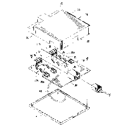
Figure 1 is a perspective view of a surge protector
module, constructed in accordance with the principles of the
present invention;
CA 02247671 1998-09-18
-8- CASE 7242 CIP
Figure 2 is a view similar to Figure 1, but with the
housing cover and base removed;
Figure 3 is an exploded perspective view of the
surge protector module of Figure 1;
Figure 4 is a detailed schematic circuit diagram of
one of the circuit surge protector devices of the present
invention;
Figure 5 is a top plan view of the printed circuit
board with the electrical components removed,
illustrating the layout of certain ones of the conductive
traces;
Figure 6 is a bottom plan view of the printed
circuit board, illustrating the layout of certain other
ones of the conductive traces;
Figure 7 is a top plan view of the printed circuit
board, illustrating the combined layout of the conductor
traces of Figures 5 and 6;
Figure 8 is a view similar to Figure 2, illustrating
a second embodiment of the present invention;
CA 02247671 1998-09-18
-9- CASE 7242 CIP
Figure 9 is a view similar to Figure 2 , illustrating
a third embodiment of the present invention;
Figure 10 is a detailed schematic circuit diagram of
a second embodiment of a circuit surge protector device
of the present invention; and
Figure 11 is a detailed schematic circuit diagram of
a third embodiment of a circuit surge protector device of
the present invention.
s
DESCRIPTION OF THE PREFERRED EMBODIMENTS
It is to be distinctly understood at the outset that
the present invention shown in the drawings and described
in detail in conjunction with the preferred embodiments
is not intended to serve as a limitation upon the scope
or teachings thereof, but is to be considered merely an
exemplification of the principles of the present
invention.
Referring now in detail to the various views of the
drawings and in particular to Figures 1-3, there is
illustrated a surge protector module of the present
CA 02247671 1998-09-18
-10- CASE 7242 CIP
invention which is designated generally by reference
numeral 10 for protecting telecommunications equipment
from power and transient surges occurring on tip and/or
ring conductors of transmission lines connected thereto.
The surge protector module 10 is utilized to protect
sensitive communications equipment up to 4-pair of wires
(8 conductors) from transient power impulses for each
pair of wires. The surge protector module has been
uniquely designed so as to meet the maximum allowable
transmission loss due to internal wiring of a building
a
and connectors according to TIA specification for
Category 5 (specification #568A for connectors).
The surge protector module 10 has a substantially
box-like configuration, although other-shaped construc-
tions can be likewise utilized. The surge protector
module includes a molded housing 12 made of a suitable
plastic material, such as non-polycarbonate and the like
which is comprised of a co-mating base member 14 and a
cover member 16. The cover member 16 can be suitably
secured to the base member 14 in any number of conven-
tional means known in the art.
CA 02247671 1998-09-18
-11- CASE 7242 CIP
The base member 14 has a generally rectangular
configuration and has a flat surface which is adapted to
mount a printed circuit boaid sub-assembly 18. The cover
member 16 is provided with opposed side walls 20 and
opposed end walls 22, respectively. The side and end
walls 20 and 22 define a cavity 24 for receiving and
enclosing the printed circuit board sub-assembly 18
mounted on the base member 14.
The printed circuit board sub-assembly 18 includes
a printed circuit board 26, a plurality (4) of circuit
surge protector devices 28a-28d, an input connector means
30, an output connector means 32, and a ground shield 34.
The input conductor means 30 is preferably disposed
adjacent the top end of the printed circuit board 26, and
the output connector means 32 is preferably disposed
adjacent the bottom end of the printed circuit board 26.
The input connector means can be any number of com-
mercially available connectors well known in the art.
For example, for telecommunication equipment the input
connector means is comprised preferably of a pair of
AT&T 110 terminal connectors 36 each having a 4-position
so that they can together accommodate up to 4-pairs of
CA 02247671 1998-09-18
-12- CASE 7242 CIP
incoming telephone lines of a telephone trunk cable (not
shown) from either a central office outside the service
area or from a distribution panel within the building.
Similarly, the output connector means can be a
number of different types and is preferably a stan-
dardized modular jack 38 referred to as an 8-position RJ-
45 jack for terminating 4 wire-pair telephone line cord.
The modular jack 38 is adapted to receive a standardized
modular plug connectible to individual telephone
equipment. The input and output connector means provide
for quick and easy mechanical connections to the four
sets of circuit surge protector devices 28a-28d located
on the printed circuit board 26.
In order to facilitate the functioning of the
circuit surge protector devices 28a-28d disposed on the
printed circuit board 26 as well as to provide a dis-
charge path to earth ground for the power and transient
surges, a ground wire 40 has its one end operatively
connected to the protector devices and its other end
connectible to an external common grounded bus (not
shown): The ground wire 40 is preferably disposed so as
CA 02247671 1998-09-18
-13- CASE 7242 CIP
to extend through one of the side walls 20 of the housing
12 .
The present invention relates to the structure of
the surge protector module 10 containing the four (4)
sets of circuit surge protector devices 28a-28d mounted
on the printed circuit board 26 in conjunction with the
method of fabricating the plurality of conductive traces
on the printed circuit board in order to meet the TIA
specification for Category 5. A detailed schematic
circuit diagram of one set of the circuit surge protector
devices 28a-28d is illustrated in Figure 4 of the
drawings. Since each set of the protector devices is
identical in its construction, it is believed sufficient
to describe in detail only one of them.
As can be seen from Figure 4, the circuit surge
protector device 28a is comprised of four banks 42, 44,
46 and 48 of rectifier diodes and a pair of voltage
suppressors 50, 52. The input side of the protector
device 28a is connectable between two wires of incoming
telephone transmission lines applied across an input tip
terminal 54 and an input ring terminal 56 defining an
unprotected side. The output side of the protector
CA 02247671 1998-09-18
-14- CASE 7242 CIP
device 28a is connectible between two wires of individual
telephone equipment to be protected applied across an
output tip terminal. 58 and an output ring terminal 60
defining a protected side.
Each of the four banks 42-48 of diodes is comprised
of three (3) low capacitance diodes connected in
parallel. The first bank 42 is formed of three diodes D1
connected in parallel with their common cathodes
connected together at node A and further joined to a
first conductor lead. The first conductor lead in the
present invention takes the physical form of a tip or
first conductive trace 62. The common anodes of the
diodes Dl are also connected together B and further
joined to a second conductor lead. The second conductor
lead takes the physical form of a second conductive trace
63. The second bank 44 is formed of three diodes D2
connected in parallel with their common cathodes con-
nected together at node C and further joined to a third
conductor lead. In the present invention, the third
conductor lead takes the physical form of a third or ring
conductive trace 64. The common anodes of the diodes D2
are also connected together at the node B and to the
second~conductive trace 63.
CA 02247671 1998-09-18
-15- CASE 7242 CIP
Similarly, the third bank 46 is formed of three
diodes D3 connected in parallel with their common anodes
connected together at node D and further joined to the
first conductive trace 62. The common cathodes of the
diodes D3 are also connected together at node E and
further joined to a fourth conductor lead. The fourth
conductor lead takes the physical form of a fourth
conductive trace 65. The fourth bank 48 is formed of
three diodes D4 connected in parallel with their common
anodes connected together at node F and further j oined to
t
the third conductive trace 64. The common cathodes of
the diodes D4 are also connected together at the node E
and to the fourth conductive trace 65. Each of the
diodes D1-D4 in the respective banks 42-48 can be similar
to the types 1N5408 or CSS02003 which have a low capaci-
tance.
The first voltage suppressor 50 has its one end
connected to the second conductive trace 63 and its other
end connected to a ground source GND via a ground
conductor lead. In the present invention, the ground
conductor lead takes the physical form of enlarged
common-ground conductive area 66. Similarly, the second
voltage suppressor 52 has its one end connected to the
fourth conductive trace 65 and its other end connected
CA 02247671 1998-09-18
-16- CASE 7242 CIP
also to the enlarged common-ground conductive area 66.
Each of the voltage suppressors 50 and 52 may be formed
of a silicon avalanche suppressor (SAS), sidactor, gas
tube, or Zener diode. In the preferred embodiment, the
voltage suppressors 50, 52 are silicon avalanche
suppressors similar to type 1.5KE.
The fabrication technique for the conductive traces
62-65 on the printed circuit board for mounting the surge
protector device 28a is best understood by reference to
Figures 5-7 of the drawings. In order to meet the TIA
specification for Category 5, the inventors have
determined that the loop (series) impedance of the surge
protector device must be made to be as small as possible
so as to extend the bandwidth of the transmission line
connected thereto and to minimize the attenuation. In
other words, the series resistance and inductive
reactance in the tip or first conductive trace 62 and in
the ring or third conductive trace 64 must be made very
small. It has been found that this can be achieved by
increasing the width of the conductive traces 62 and 64,
by maintaining the length of these traces to be as short
as possible, and by maintaining the conductive traces to
be relatively straight.
CA 02247671 1998-09-18
-17- CASE 7242 CIP
Further, it has been determined by the inventors
that the line-to-line (parallel) impedance must be made
as large as possible in order to likewise extends the
bandwidth of the transmission lines connected thereto.
In other words, the line-to-line capacitance between the
tip conductive trace 62 and the ring conductive trace 64
must be made to be very small. This can be accomplished
by adding low capacitance diodes (i.e., D1, D4) in series
with the capacitance due to the voltage suppressors 50,
52. While each bank of diodes is shown to contain three
t
diodes, they may have any number of diodes dependent upon
the amount of capacitance to be added as well as the
amount of surge current to be experienced.
As can best be seen from Figures 5-7, the tip
conductive trace 62 has been located on the top side 68
of the printed circuit board 26 and that the ring
conductive trace 64 has been located on the bottom side
70 of the printed circuit board. The conductive traces
62 and 64 are preferably positioned to be as close as
possible to each other, but not so they overlap each
other. If the distance between the traces 62 and 64 is
too far apart, there will be produced an excessive amount
of inductive reactance. If the conductive traces 62 and
64 tend to overlap each other, there will be produced an
CA 02247671 1998-09-18
-18- CASE 7242 CIP
excessive amount of capacitive reactance. In each
instance, the bandwidth of the protector will be lowered.
It should be apparent to those skilled in the art
that the criteria set forth above with respect to the
conductive traces 62 and 64 for the first set of surge
protector devices 28a applies equally as well to the
corresponding traces for the second, third and fourth
surge protector devices 28b-28d. Accordingly, the
pattern of conductive traces 62 and 64 for each set of
the surge protector devices is formed on the printed
circuit board 26 as illustrated in Figures 5-7 so as to
cooperate with the electrical components mounted thereon
in order to meet the TIA specification for Category 5.
In addition, it has been determined by the inventors
that in order to meet the crosstalk criteria (NEXT) for
Category 5 the pair-to-pair impedance must be increased.
In other words, the capacitance between the adjacent
pairs of conductive traces 62, 64 for each set of surge
protector devices must be decreased to a small value.
This was found to be accomplished by increasing the
distance between adjacent pairs. Further, by providing
the ground shield 34 between the second and third pairs
CA 02247671 1998-09-18
-19- CASE 7242 CIP
of conductive traces, this was found to improve the
crosstalk therebetween.
In Figure 8, there is shown a second alternate
embodiment for the printed circuit board sub-assembly.
It can be seen that the printed circuit board sub-
assembly 118 is substantially identical to the printed
circuit board sub-assembly 18 of Figure 2, except that
there are two additional ground shields provided. A
a
second ground shield 34a is disposed between the first
and second adjacent pair of conductive traces. A third
ground shield 34b is disposed between the third and
fourth pair of conductive traces.
In Figure 9, there is shown a third alternate
embodiment for the printed circuit board sub-assembly.
It can be seen that the printed circuit board sub-
assembly 218 is substantially identical again to the
printed circuit board sub-assembly 18 of Figure 2 , except
that the ground shield 34 has been replaced by an
elongated slot 34d defining an air gap introduced between
the second and third adjacent pairs of conductive traces.
Since 'air has a lower dielectric constant than the
material used to form the printed circuit board, the
CA 02247671 1998-09-18
-20- CASE 7242 CIP
dielectric constant between the second and third pairs of
conductive traces will be decreased and thus the
capacitance will also be decreased, thereby improving the
crosstalk therebetween.
S From the foregoing detailed description, it can thus
be seen that the present invention provides a surge
protector module for protecting telecommunication
equipment and the like from power surges which includes
a two-piece interfitting housing which receives a printed
circuit board for mounting four sets of circuit surge
protector devices, an input connector means connected to
an exposed side and an output connector connected to a
protected side. The surge protector module is charac-
terised by a small series impedance and a large line-to-
line impedance. The printed circuit board has a unique
pattern of conductive traces for mounting the electrical
components of the protector devices so as to meet the TIA
specification for Category 5.
In Figure 10, there is illustrated a second
embodiment of a circuit surge protector device 28b
defining a hybrid circuit of the present invention. All
of the circuit elements in the second embodiment of
CA 02247671 1998-09-18
-21- CASE 7242 CIP
Figure 10 are identical to the ones used in the protector
device of Figure 4 with the additon of a second voltage
suppressor consisting of two series-connected gas tubes
GT1 and GT2. In particular, the two series-connected gas
tubes GT1 and GT2 are also connected between the incoming
telephone transmission lines applied across the input tip
terminal 54 and the input ring terminal 56. Further, the
gas tubes are connected in parallel with the four banks
42-48 of the rectifier diodes D1-D4 and the pair of
voltage suppressors 50,52. The junction of the gas tubes
are joined to a ground potential GND.
In operation, upon the occurrence of a power and
transient surge across the tip and ring terminals 54 and
56 the first voltage supressors 50,52 will initially
clamp the surge to ground within a few nanoseconds.
Then, the second voltage supressors formed of the gas
tubes GT1,GT2 will subsequently fire and divert the
balance of the surge to ground. As a result, when the
protector device 28b is used in conjunction with the
fabrication technique for the conductive traces 62-65 on
the printed circuit board 26 it will meet the TIA 568A
specification for Category 5 and will produce a very fast
response time of a few nanoseconds along with the
capability of handling higher energy surges.
CA 02247671 1998-09-18
-22- CASE 7242 CIP
In Figure 11, there is illustrated a third
embodiment of a circuit surge protector 28c defining a
Category 5 gas tube protector. The surge protector 28c
consists of two series-connected gas tubes GT3 and GT4.
One end of the gas tubes is connected to both the input
tip terminal 54 and the output tip terminal 58. The
other end of the gas tubes is connected to both the input
ring terminal 56 and the output ring terminal 60. The
junction of the gas tubes is connected to the ground
potential GND. Since the capacitance of the gas tubes
are relatively low in the range of 1-2 nanofarads, there
has beem eliminated the need of the diode banks 42-48 in
order to further the capacitance. As a consequence, when
the protector device 28c is used in conjunction with the
fabrication technique for the conductive traces 62,64 on
the printed circuit board 26 it will still meet the TIA
568A specification for Category 5, but will produce a
slower response time (e.g. a few microseconds) than the
first voltage suppressors 50,52.
While there has been illustrated and described what
are at present considered to be preferred embodiments of
the present invention, it will be understood by those
skilled in the art that various changes and modifications
CA 02247671 1998-09-18
-23- CASE 7242 CIP
may be made, and equivalents may be substituted for
elements thereof without departing from the true scope,nf
the invention. In addition, many modifications may be
made to adapt a particular situation or material to the
teachings of the invention without departing from the
central scope thereof. Therefore, it is intended that
this invention not be limited to the particular embodi-
ments disclosed as the best modes contemplated for
carrying out the invention, but that the invention will
include all embodiments falling within the scope of the
appended claims.