Note: Descriptions are shown in the official language in which they were submitted.
CA 02247744 1998-09-21
ID 0679
KC Byron 71
WRITING BRAGG REFLECTION GRATINGS IN OPTICAL
WAVEGUIDES
BACKGROUND OF THE INVENTION
This invention relates to the writing of Bragg reflection gratings in
optical waveguides by exercise of the photorefractive effect in
materials, such as germania doped silica. An early method of writing
such gratings is described in United States Patent No. 4 474 427, this
method involving directing intense ultra-violet light into one end of a
length of optical waveguide having a reflector at the far end so that a
standing wave is set up within the waveguide. Subsequently, a lateral
method of writing such a grating was disclosed in United States Patent
No. 4 725 110 in which a beam-splitter is used to divide a beam of
ultra-violet light into two beams which are reflected in two mirrors to
form and interference fringe pattern in the waveguide. This writing
mçthod is sometimes known as the holographic.method. A further
alternative method, sometimes known as the grating method, involves
~ 15 creating an equivalent fringe pattern close behind a-diffraction grating
illuminated with normally incident ultra-violet light, this method being
described for instance in United States Patent No. 5 351 321.
Typically a phase grating is employed for this purpose, and the depth
of the grating elements chosen for suppression of the zero order
diffraction. The waveguide is located close behind the diffraction
grating because it is here that the required fringe pattern, which is
generated by interference between the +1 and -1 diffraction orders, is
least disrupted by power diffracted into higher order modes.
CA 02247744 1998-09-21
An exception to this close proximity arrangement of diffraction grating
and waveguide is described in the paper by J R Armitage entitled,
'Fibre Bragg Reflectors written at 262nm Using a Frequency
Quadrupled Diode-Pumped Nd3+:YLF Laser', Electronics Letters, 24th
S June 1993 Vol. 29, No. 13, pages 1181 - 3. In this instance the +1
and -1 diffraction orders are arranged to be incident upon a fused
silica block. After reflection in the side walls of this block, the two
beams emerge from the far end of the block and form an interference
fringe pattern in the core of an optical fibre waveguide located behind
10 the block. One advantage of this greater separation between the
diffraction grating and the waveguide is that it enables a zero order
beam stop to be located on the fused silica block to prevent any zero
order light from reaching the fringe pattern generated by the
interference between the +1 and -1 diffraction orders and thereby
15 reducing the visibility of that fringe pattern.
SUMMARY OF THE INVENTION
It is an object of the present invention to provide a method of writing a
Bragg reflection grating in an optical waveguide using a diffraction
20 grating !ocated at a sufficient distance from the waveguide as to make
it readily possible to include aperture defining means to control the
illumination of the waveguide so as to provide a high visibility fringe
pattern, and at the same time to use~ separated portions of the
diffraction grating -for the generation of that fringe pattern.
Particularly in the case of the writing of long Bragg reflection gratings,
- ~such use of two separated zones-of illumination of the diffra~tion -
grating has the advantage of reducing the deleterious effects in the
optical performance of the resulting Bragg reflection grating caused by
30 the presence of random stitch errors in the diffraction grating used to
write that Bragg reflection grating.
According to a first aspect of the present invention there is provided a
method of writing a Bragg grating in a photosensitive optical waveguide by
35 irradiating the waveguide with an interference fringe pattern generated by
the passage of electromagnetic radiation in two spatially separated zones
CA 02247744 1998-09-21
via a diffraction grating oriented to have diffracting elements of the
diffraction grating extending at an angle to the waveguide axis.
According to a second aspect of the present invention there is
5 provided a method of writing a Bragg grating in a photosensitive
optical waveguide by irradiating the waveguide with an interference
fringe pattern generated by the passage of electromagnetic radiation
via a diffraction grating oriented to have diffracting elements of the
diffraction grating extending at an angle to the waveguide axis,
10 wherein a beam of light is divided into two spatially separated
components arranged to be incident upon the diffraction grating in two
spatially separated zones, and the fringe pattern is generated by
interference between one diffracted order of one of the two
components and one diffracted order of the other component.
Other advantages and features of the invention will be readily
apparent from the following description of the preferred embodiments,
the drawings and the claims.
20 BRIEF DESCRIPTION OF THE DRAWINGS
.
Figure 1 is a schematic diagram of apparatus used in a prior art method
: - . of writing a Bragg reflecti~n grating,
Figure 2 is a schematic-diagram of apparatus used-in a method of
writing a Bragg reflection grating embodying the present
invention in a preferred form, and
Figure 3 is a schematic diagram of an alternative form of apparatus
used in a method of writing a Bragg reflection grating
embodying the present invention in a preferred form.
- 30
DESCRIPTION OF THE PREFERRED EMBODIMENTS
Before proceeding with the specific description of preferred
embodiments of the present invention, further reference will be made
to the prior art writing method that involves close proximity between a
CA 02247744 1998-09-21
diffraction grating and the waveguide in which the Bragg reflection
grating is to be written. This description refers to Figure 1, and is
concerned with explaining how that configuration leads to impairment
of the contrast ratio in the fringe pattern in comparison with that which
5 is attainable using the. method of the present invention.
Referring to Figure 1, a beam of intense ultra-violet light 10 is incident
normally upon a diffraction grating 11 which is typically a phase
grating whose depth is chosen to suppress the zero order diffraction of
10 normally incident light. Close behind the phase grating is located an
optical fibre waveguide 12 whose axis extends transversely with
respect to the direction of extent of the grating elements of the grating
11. The waveguide 12 is typically provided with a plastics protective
coating 1 2a, a portion of which is removed to expose the bare fibre 12
15 in the region in which the Bragg reflection grating is to be written. At
the centre of the optical fibre is its optical core 12b, the surface of
which provides the waveguiding interface of the fibre. Typically the
light of beam 10 is concentrated upon this core by means of a
cylindrical lens 13. When the light is incident upon the diffraction
20 grating is divided into a number of beams of different diffraction order.
~ Ir~ Figure. 1 just three of.those beams are depicted,. namely the ~
order diffraction beam 10a, the zero order diffraction beam 10b, and
~ the +1 order diffraction beam-10c. Within the triangular area defined
~ by the right-hand edge of the +1 order diffraction beam, the left-hand
25 edge of the -1 order diffraction beam, and the diffraction grating itself
there is complete overlap of the light of these two diffraction orders
that thereby give rise to the potential of maximum fringe contrast.
However this is diluted by any light propagating in the zero order
(which is fringeless) if such zero order light has not been completely
30 suppressed by the choice of appropriate profile of the grating
elements of grating 11. Additionally there are regions of the fibre core
12 immediately to the left of, and immediately to the right of, the
triangular region of complete overlap, where the core is exposed to
CA 02247744 1998-09-21
light of one of the first diffraction orders, but not to that of the other.
To the extent that these regions of light are devoid of the requisite
fringe pattern, they create undesirable pedestals in the refractive index
changes induced in the core by the photorefractive effect of the
5 exposure to the ultra-violet light.
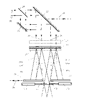
Attention is now turned to the writing of a Bragg reflective grating in
the core of optical fibre waveguide using the apparatus of Figure 2
and embodying the present invention in a preferred form. The light of
10 beam 10 is divided into two substantially equal amplitude components
10l and 10ll by means of a beam-splitter 20, these two components
being incident, after reflection in mirrors 21 and 22, and optionally
after passage through a cylindrical lens 23, normally upon the
diffraction grating 11 in two spaced apart regions. This grating may be
15 a uniform pitch grating or a chirped on. For the writing of a uniform
pitch Bragg reflection grating it will be a uniform pitch grating. In the
same way that beam 10 of Figure 1 is divided into a number of beams
of different diffraction order as the result of being incident normally
upon the diffraction grating 11, the normally incident light of
20 - component beams 10l and 10ll is similarly divided. In Figure 2 also, just
three of those beams are depicted for each component beam 10l and
10ll, namely the -1 order diffraction beams 10la and 10lla, the zero
- order diffraction beam 10lb and 10llb, and the ~1 order diffraction
beams 10lC and 10llc. A field stop 24 is placed to intercept all the
25 diffracted orders except for diffracted beams 10lC and 10lla, which pass
through this field stop. The fibre 12 is located behind the field stop at
the position where its core 12b lies where there is complete
overlapping of the diffracted beams 10lC and 10lla.. The cylindrical
lens 23, if used, is employed to focus the light on to the core 12b of
30 the fibre 12, and so performs an equivalent function to that performed
by its counterpart lens 13 of Figure 1.
CA 02247744 1998-09-21
In the course of time, the profiled surface of the phase grating 1 is
liable to contamination leading to impairment of its performance. It is
possible to remove this contamination by a special cleaning process,
5 but this is rather time-consuming. It may be preferred therefore, since
the fibre 12 is at some distance from this grating, to provide it with a
silica cover slip 25 in order to protect its profiled surface from
contamination, the exposed surface of the cover slip being capable of
being cleaned much more readily and quickly.
The apparatus of Figure 2 may be used for the writing of Bragg
reflection gratings on a static basis, in which case further masking (not
shown) may be employed for apodisation of the extremities of the
written grating. Alternatively, particularly for the writing of longer
15 Bragg reflection gratings, the apparatus may be used for writing in a
scanning mode, in which case there is ganged movement of the mirror
22 and the field stop 24 in the direction of axial extent of the fibre 12,
such ganged movement being indicated by arrows 26.
20 - One of the problems liable to be encountered in the writing of long
Bragg reflection gratings is the degradation of spectral performance
introduced by the presence of stitch errors in the spacing of the
diffracting elements of the diffraction grating employed to write that
Bragg grating. These stitch errors are particularly liable to arise when
25 the diffracting elements of the diffraction grating are themselves
written in batches on a step-and-~repeat basis for instance using
E-beam lithographic techniques. Imperfections in the stepping process
are liable to produce 'phase errors' of random magnitude between
nearest neighbour diffraction elements of adjacent batches of
30 elements. With the close proximity arrangement of diffraction grating
and optical waveguide of Figure 1, such phase errors are translated
CA 02247744 1998-09-21
-7-
with little modification from the diffraction grating to tha Bragg
reflection grating because relatively few diffraction elements of the
diffraction grating contribute significantly to the writing of any individual
element of the Bragg reflection grating. This contrasts with the
5 situation pertaining in the case of the spaced arrangement of Figure 2.
In particular it will be appreciated that, because the magnitudes of the
individual phase errors are random, there is liable to be no correlation
between a phase error present in that part of the diffraction grating
illuminated by beam 10l and one present in that part illuminated by
10 beam 10ll. This means that stitch errors in present in the diffraction
grating 11 have less deleterious effect upon the spectral performance
of Bragg reflectors written using the apparatus of Figure 2 than upon
those written using the apparatus of Figure 1.
15 It may be noted that the particular arrangement of beam-splitter 20,
and mirrors 21 and 22 of Figure 2 provides a noticeably unequal
optical path difference in respect of the two pathways from the beam-
splitter to the fibre core 12b. This can be a problem if the source of
ultra-violet light providing beam 10 has a short optical coherence
20 length. Figure 3 shows a modified arrangement in which,-in order to
- equalise the optical path length, the single mirror 22 has been
replaced by a pair of mirrors 32a and 32b and the beam-sp!itter 20
and mirror 21 have been - reoriented. In all oth-er respects the
components of the apparatus of Figure 3 are in essence identical with
25 their counterparts in the apparatus of Figure 2.