Note: Descriptions are shown in the official language in which they were submitted.
CA 02247794 1998-09-25
GRAY-SCALE DRIVER FOR FIXED-INTENSITY ELECTRONIC DISPLAY
1. Field of the Invention:
This invention relates to a method and driver for
driving fixed-intensity electronic displays in such a way
as to produce multiple levels of intensity (gray-scale)
on a per-pixel basis. It applies in particular, but not
exclusively, to built-in driver vacuum fluorescent
display (BDVFD) products.
2. Description of the Prior Art:
Some electronic displays are only available with
fixed-intensity electronic drive circuitry, i.e. the
pixels can only be driven in one of two states (bi-
stable). A good analogy for the pixels of these displays
would be a lamp that only has a simple on-off switch,
while a lamp controlled by a dimmer would not fill that
category since it can directly provide intermediate
brightness levels. It should be noted that the word
"pixel" refers to a picture element which is the smallest
addressable component of the display.
This is the case, for example, of the BDVFD products
manufactured by the Japanese company Noritake, which
constitute an improvement on the previous generation of
vacuum fluorescent display (VFD) devices by integrating
within the glass display package the electronic driver
circuits. VFDs act as a classic triode vacuum tube, with
a cathode filament emitting electrons when heated, an
anode at a relatively high voltage (around 55 volts) and
a grid between the anode and cathode. In Noritake~s VFDs,
-1-
CA 02247794 1998-09-25
the triode is used only in two discrete states, fully ON
or fully OFF, because logic circuits are used to control
them. In the OFF state, the grid is driven at a voltage
below that of the cathode to stop the electron flow from
cathode to anode. In the ON state, the grid switches to a
higher voltage than the cathode: the electrons are drawn
toward the anode, hit the phosphor coating which emits
the light. The phosphor used by Noritake emits a
blue-green light when excited. Since the built-in driver
circuit either switches the grid fully ON or fully OFF,
it has no provision for varying the intensity of light on
a per-pixel basis.
The standard circuit recommended by Noritake for
controlling their BDVFD devices includes sections for
power supply and logic waveform generation. The power
supply must provide different voltages for the anodes
(approximately 55 volts, Direct Current) and cathodes
(approximately 4 volt RMS of Alternating Current,
centered around the 6 volt DC level, to heat the
filaments). The built-in driver inside the Noritake
display receives logic data from the control inputs as a
stream of serially shifted 0's and 1's, for two columns
of pixels on the screen, then switches ON the grids for
these columns while the data for the next two columns is
shifted in. Eventually, all the pixels get addressed this
way, to be turned on briefly if their corresponding data
was a 1. The required refresh rate for the display (the
addressing of all of its pixels) should be at a minimum
-2-
CA 02247794 1998-09-25
of one hundred times per second to prevent flicker.
OBJECTS AND SUMMARY OF THE INVENTION
It is an object of the present invention to improve
upon present fixed-intensity electronic displays by
providing multiple levels of intensity or gray-scale
therefor, thus allowing for display of shades in such
devices.
Another object is to achieve intermediate intensity
levels in BDVFD products.
Other objects and advantages of the present
invention will be apparent from the following description
thereof .
The invention basically relies on inertia inherent
to either the human vision neurosystem (referred simply
as the eye hereafter) or the display technology used. The
inertia of the eye is defined as the maximum speed at
which changes in light intensity can be perceived. The
peripheral vision is more sensitive to fast, small
changes in light intensity and is used to measure the
maximum rate of detectable changes in light intensity. If
a point in the field of view changes states faster than
this limit, the eye perceives a light intensity that is
an intermediate value between the two states. The inertia
of the display relates to some property, either
mechanical, chemical or physical, that causes the pixels
to resist abrupt changes in their state. Fluorescent
lamps have negligible inertia compared to that of the
human eye because luminosity ceases as soon as the
-3-
CA 02247794 1998-09-25
excitation is removed, while phosphorescent materials
(such as those used in the cathode ray tube of a TV or
computer monitor) exhibit a decaying light output, called
persistence, after the excitation stops.
The perceived light value from a point is the sum of
all contributing emitted, reflected or refracted light
sources. If two light sources vary their intensities at
rates A and B, both above the rate detectable by the
human eye, they could still exhibit a beating effect at a
rate ~A - B~ that could be below the detectable rate, and
therefore be observable; this is the principle behind
stroboscope tachometers. This beating effect can be
observed with computer monitors that have a refresh rate
below 85 Hz in offices lit by fluorescent lamps (which
have a frequency of 60 Hz in North America); this
undesirable effect is called screen flicker and is most
perceptible with a large white screen background.
The essence of the present invention is to have a
much faster screen refresh rate and alternate between the
ON and OFF states for each pixel according to the
intermediate intensity level desired. The persistence of
both the phosphor and human eye have an integrating (or
averaging) effect on the intensity of the light emitted
by the pixel and perceived by the observer. The perceived
light intensity is directly controlled by the proportion
of the time that the pixel is ON.
By sequencing several fields in which the pixels may
have different states, at a rate that is at least double
-4-
CA 02247794 1998-09-25
and preferably several times the normal minimum refresh
rate, there is obtained the desired averaging effect and
the perception of different intensities (or shades of
blue-green) for each pixels. The number of fields defines
the number of intensities perceived (plus one for the
all-off, or black, intensity). Also, by spreading the ON
states as much as possible over time, the chances of
perceptible flicker are minimized.
BRIEF DESCRIPTION OF THE DRAWINGS
A non-limitative embodiment of the present invention
will now be described with reference to the appended
drawings, in which:
Fig. 1 shows a timing diagram that illustrates pixel
state to field for each of 8 equally spaced brightness
levels; and
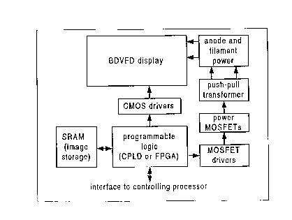
Fig. 2 shows a block diagram of a BDVFD module
provided with the improved features of the present
invention.
DETAILED DESCRIPTION OF THE INVENTION
The timing diagram of Fig. 1 illustrates one
embodiment of the method of relating pixel state to
field, for each of 8 equally spaced brightness levels
from 0% (black) to 100% (full intensity). The ON states
are deliberately spread over the repetitive period (the
full sequence of fields) to minimize flicker. There could
be some flicker remaining for the 14% intensity since it
has only one ON state per repetitive period. The effect
-5-
CA 02247794 1998-09-25
of this artifact is minimized since it occurs for the
lowest intensity above the black level.
The block diagram of Fig. 2 illustrates one
embodiment of the circuit that the applicant has
implemented to validate the above described concept. It
works off a single regulated 5V DC power supply. The
included power circuitry uses a push-pull transformer
drive whose duty cycle (and thus output levels) can be
varied under software control for overall intensity
control of the display.
The implementation described herein uses 4 bits of
memory for each pixel. The controlling processor writes
and reads the display memory while the display refresh
circuitry only reads it. The logic allows synchronized
accesses to the memory by both the processor and refresh
circuitry.
For each pixel, one bit of memory is used to control
blinking (turning the pixel ON and OFF at a slow rate)
while the other three define which of the 8 possible
shades is displayed (OOOb for black, lllb for maximum
intensity).
In the diagram of Fig. 2, the various acronyms have
the following meanings:
BDVFD - built-in driver vacuum fluorescent display
CMOS - complimentary metal oxide semiconductor
SRAM - static random access memory
MOSFET - metal-oxide-semiconductor field effect
transistor
CPLD - complex programmable logic device
FPGA - field programmable gate array.
-6-
CA 02247794 1998-09-25
The above terms are generally known in the art.
The circuit illustrated in Fig. 2 has a refresh
circuitry (consisting of SRAM, programmable logic and
CMOS drivers) that enables much faster refresh rate and
alternating between ON and OFF states than was previously
proposed for fixed intensity electronic displays. Thus,
the rate can be at least 200 times per second for 3
intensities, at least 300 times per second for 4
intensities and at least 400 times per second for 8
intensities with minimal flicker as illustrated in Fig.
1. It has been found, however, that for the BDVFD display
arrangement shown in Fig. 2, the maximum field refresh
rate is 420 times per second (Hz) which for seven fields
(eight intensities) produces 60 full image refresh
(screens) per second.
It should be noted that the invention is not limited
to the specific embodiments described above, but that
various obvious modifications can be made by those
skilled in the art without departing from the invention
and the scope of the following claims.