Note: Descriptions are shown in the official language in which they were submitted.
CA 02248066 1998-09-23
ELECTROMAGNETIC RADIATION SHIELD MATERIAL AND PANEL
AND METHODS OF PRODUCING THE SAME
8ACKGROUND OF THE INVENTION
Field of the Invention
This invention relates to a transparent
electromagnetic radiation shield material and a transparent
electromagnetic radiation shield panel for placement in
front of a display device or other such source of
electromagnetic radiation to shield the viewer from
electromagnetic radiation, and to methods of producing the
material and panel. It particularly relates to a panel
suitable for a large plasma display.
Description of the Background Art
An electromagnetic radiation shield panel for
placement in front of a display device or other source of
electromagnetic radiation is required to have not only
excellent electromagnetic radiation shielding capability
but also excellent transparency (optical transmittance),
good clarity (degree of coating blackness etc.), wide
viewing angle and the like. Japanese Patent Application
Laid-Open No. 9-298384 teaches an electromagnetic radiation
shield panel meeting these requirements to some extent.
Specifically, this laid-open patent application teaches a
method wherein "a step of providing a black dyed layer on
a transparent base material, a step of providing a metallic
layer on the black dyed layer, a step of providing a
27076-13
CA 02248066 1998-09-23
patterned resist layer on the metallic layer and a step of
removing portions of the metallic layer not covered by the
resist layer by etching with an etching solution are
conducted in succession, portions of the black dyed layer
not covered by the patterned metallic layer being decolored
in the etching step."
Generally, however, a sufficient degree of
coating blackness and good clarity are hard to obtain when
a black dye is used in a black resin layer. The dye
content and/or the resin layer thickness therefore has to
be increased.
Moreover, when the etching solution for the
metallic layer is used to decolor and extract the black
dye, the metallic layer comes to be over-etched owing to
the long time needed for the decoloration.
SUMMARY OF THE INVENTION
For overcoming the aforesaid drawbacks of the
prior art, this invention provides:
An electromagnetic radiation shield material
comprising at least a mesh-like metallic foil layer, a
black resin portion of identical mesh-like pattern to the
metallic foil layer and in aligned contact therewith, and
a transparent base material;
An electromagnetic radiation shield panel
comprising a laminated composite of an electromagnetic
radiation shield material and a display panel or a
-- 2
CA 02248066 1998-09-23
transparent base material, a metallic foil of the
electromagnetic radiation shield material being disposed on
the side intended to face a source of electromagnetic
radiation and a black resin portion being disposed outward
of the metallic foil;
A method of producing an electromagnetic
radiation shield material comprising a step of providing in
order on a transparent base material a black resin layer
including a black pigment, a metallic foil layer, and a
mesh-like resist layer, a step of etching metallic foil
portions not protected by the resist layer to impart the
metallic foil with a mesh-like pattern like the resist, and
a step of extracting and removing black pigment from a
portion of the black resin layer not in contact with the
mesh-like metallic foil layer to form a black resin
portion, and;
A method of producing an electromagnetic
radiation shield material comprising a step of providing in
order on a transparent base material an adhesive layer, a
black resin layer including a black pigment, a metallic
foil layer, and a mesh-like resist layer, a step of etching
metallic foil portions not protected by the resist layer to
impart the metallic foil with a mesh-like pattern like the
resist, and a step of extracting and removing black pigment
from a portion of the black resin layer not in contact with
the mesh-like metallic foil layer to form a black resin
portion.
CA 02248066 1998-09-23
When the transparent base material is a
continuous web (roll) of film, sheets of different sizes
can be cut from the obtained transparent electromagnetic
radiation shield film while avoiding inclusion of defective
portions, whereafter the cut sheets can be easily laminated
to display panels or transparent base plates. By this, the
invention can achieve high yield and low cost. Since the
roll film can be produced by a continuous process, its
productivity is higher than when the transparent base
material is plate-like. Owing to its flexibility,
moreover, the film can also be used to produce curved
shields.
In accordance with another aspect- of the
invention, a transparent electromagnetic radiation shield
panel is produced by laminating a transparent
electromagnetic radiation shield film to a display panel or
a transparent base plate by an intervening adhesive layer
on the surface of the electromagnetic radiation shield
layer.
BRIEF EXPLANATION OF THE DRAWING
Figure 1 is partial sectional view of one example
of an electromagnetic radiation shield material according
to the invention.
CA 02248066 1998-09-23
DETAILED DESCRIPTION OF THE PREFERRED EMBODIMENTS
The base material used in this invention is
required to be transparent. It is selected according to
intended use from among various materials including, for
5 example, glass plate, plastic film, plastic sheet and
plastic plate. The shape of the base material is not
particularly limited.
A plastic used as the base material is preferably
a resin with high transparency. Preferable examples
10 include acrylic resins, polycarbonate, polyethylene, AS
resins, vinyl acetate resin, polystyrene, polypropylene,
polyester, polysulfone, polyethersulfone,
polyvinylchloride, olefine-maleimide copolymer, and
norbornene resins. Among these, olefine-maleimide
15 copolymer and norbornene resins are particularly preferable
owing to their high heat resistance.
The plastic should preferably have a thermal-
deformation temperature of 140-360 ~C, a coefficient of
thermal linear expansion of not greater than
20 6. 2xlO-5cm/cm- ~C, a pencil hardness of not less than 2H, a
bending strength of 1,200-2,000 kgf/cm2, a modulus of
elasticity in bending of 30, 000-50, 000 kgf/cm2, and a
tensile strength of 700-1,200 kgf/cm2. A plastic with these
properties is resistant to high-temperature warping and
25 scratching, and can therefore be used in a wide range of
environments .
CA 02248066 1998-09-23
The plastic preferably has an optical
transmittance of not less than 90 %, an Abbe's number of
S0-70 and a photoelasticity constant (glass region) of an
absolute value of not greater than lOxlO~13cm2/dyne. A
plastic with these properties exhibits high transparency
(is bright) and little birefringence (is not likely to
produce a double image), and therefore does not degrade the
image quality, brightness etc. of the display.
The metallic foil used in this invention is not
particularly limited regarding type or thickness insofar it
has electromagnetic radiation shielding capability and can
be etched. Preferable examples include copper, nickel,
iron, stainless steel, titanium, aluminum and gold. Among
these, copper foil is particularly preferable from the
points of shielding property (resistivity) and etchability.
A thicker metallic foil is generally better in shielding
performance and a thinner one better in etchability. In
the case of a copper foil, since the shielding performance
does not change substantially at thicknesses above 5 ~m,
one of a thickness of 5-35 ~m, preferably 9-18 ~m, is
ordinarily used in consideration of handling ease and cost
per unit area (18 ~m copper foil currently being cheapest).
The pattern and aperture ratio of the metallic
foil are not particularly limited insofar as they are
within ranges ensuring sufficient electromagnetic radiation
shielding performance and optical transmittance. Even a
parallel line pattern, for example, provides shielding
CA 02248066 1998-09-23
effect (exhibiting directionality in the near field).
Since the effect is insufficient, however, a mesh pattern
is ordinarily used. Various basic mesh patterns are
available, including grid (tetragonal), triangular,
polygonal, circular and elliptical.
The aperture ratio (the ratio of the non-metallic
foil portion area relative to the repeated pattern unit
area) is determined by the line width and interval (opening
width) of the metallic foil pattern. Different patterns
with the same aperture ratio have the same optical
transmittance. Since the electromagnetic radiation
shielding performance increases with decreasing opening
width, however, a narrower opening width is ordinarily
preferable. Nonetheless, the opening width is finally
decided to fall within the range that does not cause
occurrence of Moiré fringes when the electromagnetic
radiation shielding is disposed on the front of the display
panel.
The resin in the resin solution containing the
black pigment (the black coating liquid) applied to the
metallic foil is not particularly limited by type insofar
as it is transparent and is capable of efficiently
dispersing or dissolving the black pigment.
Since the black pigment in the black coating is
extracted and removed chiefly in aqueous solution, the
resin used is preferably a hydrophilic transparent resin.
Preferable hydrophilic transparent resins include vinyl
CA 02248066 1998-09-23
acetal resins, vinyl alcohol resins, acrylic resins,
cellulose resins and the like. Among these, vinyl acetal
resins such as polyvinyl butyral and cellulose resins such
as cellulose acetate butylate are particularly preferred.
The black pigment used in this invention consists
of reduced metal particles or metal oxide particles. The
reduced metal particles are colloid particles contained in
a reduced metal colloid dispersion or reduced metal powder
particles obtained from the metal colloid dispersion. They
are not particularly limited as regards type of metal or
grain size insofar as they are uniformly dispersable in the
coating liquid (coating) and do not impair the coating
transparency after extraction and removal. For easy
extraction, however, the grain size of the reducing metal
particles is preferably not greater than 1 ~m. They
preferably have high stability with respect to the
atmosphere and moisture.
Specific examples of usable reduced metal
particles include particles of metals belonging to Group Ib
or Group VIII of the Periodic Table of the Elements (Cu,
Ni, Co, Rh, Pd etc.), with reduced Pd colloid particles and
reduced Pd powder obtained therefrom being particularly
preferable. The reduced metal colloid particles can be
produced by the methods described in Japanese Patent
Application Laid-Open No. 1-315334. Specifically, a
colloid dispersion can be obtained by reducing a salt of
-- 8
CA 02248066 1998-09-23
the metal in a mixed solution consisting of a lower alcohol
and an aprotic polar compound.
The metal oxide particles are not particularly
limited as regards type of metal or grain size insofar as
they are uniformly dispersable in the coating liquid
(coating) and do not impair the coating transparency after
extraction and removal. For easy extraction, however,
their grain size is preferably not greater than 1 ~m. The
metal oxide particles should best remain stably dispersed
in the coating liquid (coating). Preferable examples
include particles of oxides of metals belonging to Group Ib
or Group VIII of the Periodic Table of the Elements such as
iron, copper, nickel, cobalt and palladium.
The amount of these black pigments included is
preferably in the range of 1-lO0 PHR (parts by weight based
on 100 parts by weight of resin), more preferably 5-50 PHR.
When the amount used is less than 1 PHR, the degree of
coating blackness is low. An amount exceeding 100 PHR
degrades the coating property.
The solvent for the resin solution in this
invention can be of any type insofar it can dissolve or be
used to prepare a dispersion of the resin and the black
pigment.
Preferable solvents include one or a mixture of
two or more of, for example, water, methanol, ethanol,
chloroform, methylene chloride, trichloroethylene,
tetrachloroethylene, benzene, toluene, xylene, acetone,
CA 02248066 1998-09-23
ethyl acetate, dlmethylformamlde, dlmethylsulfoxlde,
dlmethylacetamlde and N-methylpyrrolldone. A solvent
approprlate for the comblnatlon of resln and black plgment ls
selected.
The amount of solvent used ls selected so as to
obtaln an approprlate vlscoslty and fluldlty and to make the
dlsperslon approprlate for appllcatlon to the base materlal.
The dlsperslon of the resln and black pigment (black
coatlng llquld) ls applled to the metalllc foll and drled to
form a coatlng contalnlng the black plgment. The appllcatlon
of the dlsperslon can be carrled out by brush coatlng,
spraylng, dlpplng, roller coatlng, calender coatlng, spln
coatlng, bar coatlng or other conventlonal method selected ln
vlew of the shape of the metalllc foll.
The condltlons (temperature, tlme etc.) for coatlng
formatlon are determlned based on the type and concentratlon
of the resln, the coatlng thlckness and the llke. The
nonvolatlle content of the solutlon ls normally 0.05-20 wt%.
The thlckness of the drled coatlng ls not partlcularly
crltlcal and ls generally 0.5-50 ~m, preferably 1-25 ~m.
Blackness may be observed only scarcely and the clarlty may
become poor at a thlckness of less than 0.5 ~m. Extractlon of
the unnecessary portlon may be more dlfflcult at a thlckness
exceedlng 50 ~m.
A lamlnated artlcle ls formed by adherlng the coated
slde of the metalllc foll formed wlth the black coatlng to a
transparent base materlal elther dlrectly or
-- 10 --
27076-13
CA 02248066 1998-09-23
via an intervening transparent adhesive. Usable
transparent adhesives include polyvinylacetate, acrylic,
polyester, epoxy and cellulose type adhesives. The
thickness of the adhesive layer is generally not less than
S 1 ~m, preferably about 5-500 ~m.
As viewed from the side of the transparent base
material (thickness: 2 mm, refractive index: 1.49, optical
transmittance: 93 %, average roughness Ra: 40 ~) of the
laminated article, the coating preferably has a degree of
blackness, expressed as optical density, of not less than
2.9 (angle of incidence of 7 ~; assuming no specular
component). When the optical density is less than 2.9,
clarity of the final transparent electromagnetic radiation
shield material is poor owing to the low blackness of the
coating. (The intensity of plating glare increases with
decreasing optical density.) When the optical density is
2.9 or greater, the blackness of the coating is adequate
and clarity excellent (definition high). Clarity as
perceived by the naked eye does not improve substantially
above an optical density of 4Ø
Next, a resist portion patterned identically to
the desired pattern of the metallic foil layer of the
electromagnetic radiation shield material is formed on the
metallic foil of the laminated article. The resist portion
can be formed by a generally known method such as printing
or photolithography. The resist portion can be either
transparent or colored.
CA 02248066 1998-09-23
Unnecessary portions of the metallic foil where
no resist is present are removed with an etching solution.
Removal of black pigment from the coating is preferably
effected by soaking in the same etching solution or a
separate acidic or alkaline treatment liquid at a
temperature of around 10-30~C for around 1-10 min. Removal
can be effected by solution spraying rather than soaking.
The removal can be promoted by application of ultrasonic
waves.
As a result, the coating is formed under the
patterned metallic foil layer with a black portion of the
same pattern. The portions where the metallic foil layer
and the black pigment in the coating have been removed is
transparent. The resist portions are then removed by
soaking in or spraying with an exfoliating solution such as
an aqueous alkali solution or other such solution capable
of dissolving the resist.
Methods that can be used to remove the black
pigment include not only the aforesaid extracting but also
laser working, sand blasting and the like.
The foregoing processes enable the fabrication of
a transparent electromagnetic radiation shield material
having a metallic foil layer formed in a desired pattern.
The transparent electromagnetic radiation shield
material preferably has an optical transmittance of not
less than 65 ~ and a shielding performance of not less than
40 dB in the range of 30 to 1000 MHz. An optical
CA 02248066 1998-09-23
transmittance of less than 65 ~ is too dark and a shielding
performance of less than 40 dB is not sufficient for
practical applications.
The etching solution is selected as appropriate
for the type of metal of the metallic foil layer. In the
case of copper foil, for example, ferric chloride or the
like can be used as the etching solution.
When the foregoing production method is applied
to a transparent film to fabricate a transparent
electromagnetic radiation shield film, the transparent
electromagnetic radiation shield film is thereafter
laminated to a display panel or a transparent base plate,
using an intervening transparent adhesive if necessary, to
fabricate a transparent electromagnetic radiation shield
panel. The transparent film is preferably one constituted
as a continuous web that can be continuously processed into
a roll. Such films include plastic films having a
thickness in the approximate range of 5-300 ~m made of
polyethylene terephthalate (PET), polyimide (PI),
polyethersulfone (PES), polyether-etherketone (PEEK),
polycarbonate (PC), polypropylene (PP), polyamide, acrylic
resin, cellulose propionate (CP), and cellulose acetate
(CA).
An example of a transparent electromagnetic
radiation shield material provided by the invention will
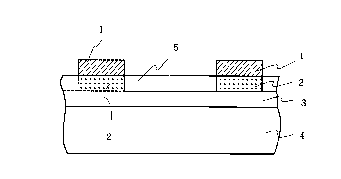
now be explained with reference to Figure 1. Figure 1 is
a sectional view showing the laminated structure of the
CA 02248066 1998-09-23
shield material, which comprises a mesh-like metallic foil
layer 1 and a transparent base material 4 sandwiching a
black resin portion 2 containing black pigment.
The transparent base material 4 and the black
resin portion 2 are adhered to each other by an intervening
transparent adhesive layer 3.
The transparent base material and the black resin
portion can instead be directly adhered without use of an
adhesive. This can be achieved, for example, by rolling,
spraying or otherwise applying molten or dissolved black
resin on the transparent base material and then drying the
applied coating.
Transparent resin 5 removed of the black pigment
by extraction is present at interstices in the black resin
portion.
Example 1.
A black coating liquid was prepared by uniformly
dispersing black pigment [A] (cupric oxide fine powder,
product of Nihon Kagaku Sangyo Co., Ltd.) in an alcohol
(ethanol) solution of polyvinylbutyral (PVB) (#6000-C,
product of Denki Kagaku Kogyo, Co., Ltd.). (Coating
solution composition: cupric oxide/PVB/ethanol
50/100/1850.)
The coating liquid was applied to one surface of
12 ~m electrolytic copper foil (CF T9 SV, product of Fukuda
Metal Foil and Powder Co., Ltd.) and dried to obtain a
- 14 -
CA 02248066 1998-09-23
black coating (25 ~m). The coated surface was laminated to
an acrylic plate (Delaglas K, product of Asahi Chemical
Industry Co., Ltd.) using an acrylic adhesive to obtain a
laminated article.
The copper foil side of the laminated article was
coated with a positive etching photoresist (PMER P-DF40S,
product of Tokyo Ohka Kogyo Co., Ltd.), prebaked, exposed,
developed and post-baked to form a resist pattern.
The resist-patterned article was soaked in
etching solution (aqueous solution of 20 % ferric chloride
and 1.75 % hydrochloric acid) to dissolve and remove the
copper foil layer at the non-resist portions, the cupric
oxide powder in the portions of the black coating exposed
by removal of the copper foil was further extracted and
removed in the same etching solution (extraction solution),
and the resist was then peeled off to produce an
electromagnetic radiation shield material.
The electromagnetic radiation shield material
exhibited shielding performance of 40-80 dB (30-1000 MHz)
and transparency (optical transmittance) of 65 %, as well
as excellent clarity (degree of coating blackness), copper
foil adherence, and base plate flatness.
Example 2.
An electromagnetic radiation sh1eld material was
fabricated in the same manner as in Example 1 except that
the cupric oxide fine powder used to prepare the black
coating liquid was replaced with black pigment (iron oxide
*
Trade-mark
27076-13
CA 02248066 1998-09-23
fine powder; Tetsuguro PO023, product of Daido Chemical
Industry Co., Ltd.) and that a 5 % aqueous hydrochloric
acid solution was used as the extraction solution for the
black pigment in the coating.
The electromagnetic radiation shield material
exhibited excellent performance characteristics similar to
those of that obtained in Example 1. It was particularly
excellent in clarity (degree of coating blackness).
Example 3.
An N-methyl-2-pyrrolidone (NMP)/ethanol solution
of palladium acetate and an ethanol solution of PVB were
mixed under stirring (and heating as required) to prepare
a reduced palladium colloid base black coating liquid.
(Coating liquid composition: palladium acetate/PVB/NMP/-
ethanol = 25/100/1250/2625.)
This coating liquid was used to fabricate an
electromagnetic radiation shield material under the same
conditions as in Example 1 except that the coating
thickness was made 10 ~m.
The electromagnetic radiation shield material
exhibited excellent performance characteristics similar to
those of that obtained in Example 1. It was particularly
excellent in clarity (transmittance: 70 %).
Example 4.
An N-methyl-2-pyrrolidone (NMP)/ethanol solution
of palladium acetate and an ethanol solution of PVB were
mixed under stirring (and heating as required) to prepare
Trade-mark
- 16 -
27076-13
CA 02248066 1998-09-23
a reduced palladium colloid base black coating liquid.
(Coating liquid composition: palladium acetate/PVB/NMP/-
ethanol = 25/100/1250/2625.)
The coating liquid was applied to one surface of
12 ~m electrolytic copper foil (CF T9 SV, product of Fukuda
Metal Foil and Powder Co., Ltd.) and dried to obtain a
black coating t10 ~m). The coated surface was laminated to
polyethylene terephthalate (PET) film using an acrylic
adhesive to obtain a laminated film.
10The copper foil surface of the laminated film was
coated with a positive etching photoresist (PMER P-DF40S,
product of Tokyo Ohka Kogyo Co., Ltd.), prebaked, exposed,
developed and post-baked to form a resist pattern. The
resist-patterned film was soaked in etching solution
15(aqueous solution of 20 % ferric chloride and 1.75 %
hydrochloric acid) to dissolve and remove the copper foil
layer at the non-resist portions, the reduced palladium
colloid particles in the portions of the coating exposed by
removal of the copper foil were further extracted and
removed in the same etching solution (extraction solution),
and the resist was then peeled off to produce an
electromagnetic radiation shield material.
A 10 ~m transparent acrylic adhesive layer was
formed on the film side of the electromagnetic radiation
shield film and the electromagnetic radiation shield film
was laminated to a glass plate (thickness: 4 mm) by the
Trade-mark
- 17 -
27076-13
CA 02248066 1998-09-23
adhesive layer to fabricate a transparent electromagnetic
radiation shield panel.
The electromagnetic radiation shield panel
exhibited shielding performance of 40-80 dB (30-1000 MHz)
and transparency (optical transmittance) of 70 %, as well
as excellent clarity (degree of coating blackness), copper
foil adherence, and base panel flatness.
ExamPle 5.
The transparent electromagnetic radiation shield
film of Example 4 was applied on its copper foil pattern
side with a transparent adhesive layer as in Example 4 and
thereafter laminated to a plasma display panel (PDP) by the
adhesive layer to fabricate a transparent electromagnetic
radiation shield panel. The electromagnetic radiation
shield panel exhibited excellent performance
characteristics similar to those of that obtained in
Example 4.
Example 6.
A transparent electromagnetic radiation shield
film was produced in the manner of Example 4 except that
the PET film of Example 4 was replaced with a triacetyl
cellulose (TAC) film laminate obtained by laminating a
protective film to TAC film via a transparent acrylic
adhesive layer.
The protective film was peeled off the
electromagnetic radiation shield film and the
electromagnetic radiation shield film was laminated to an
- 18 -
CA 02248066 1998-09-23
acrylic resin plate to fabricate a transparent
electromagnetic radiation shield panel. The
electromagnetic radiation shield panel exhibited excellent
performance characteristics similar to those of that
obtained in Example 4.
ExamPle 7.
A transparent electromagnetic radiation shield
film was produced in the manner of Example 4 except that
the PET film of Example 4 was replaced with a near infrared
(NIR) cut film.
The electromagnetic radiation shield film (the
copper foil pattern side thereof) was laminated to a glass
plate formed with a transparent adhesive layer to fabricate
a transparent electromagnetic radiation shield panel. The
electromagnetic radiation shield panel exhibited excellent
performance characteristics similar to those of that
obtained in Example 4.
Example 8.
Electromagnetic radiation shield panels were
fabricated as in Example 4 except that the acrylic plate
used as the transparent base material in Example 4 was
replaced with transparent heat-resistant plastic plates
made of olefine-maleimide copolymer (TI-160, product of
Tosoh Corporation) and norbornene resin (Arton, product of
Japan Synthetic Rubber Co., Ltd.).
The electromagnetic radiation shield panels
exhibited excellent performance characteristics similar to
Trade-mark
- 19 -
27076-13
CA 02248066 1998-09-23
those of that obtained in Example 4. They were superior to
the electromagnetic radiation shield panel of Example 4 in
base panel flatness (noticeably less warp for a base panel
of the same thickness and area).
When an electromagnetic radiation shield panel
utilizing a plastic base panel low in heat resistance and
rigidity is disposed in front of a (plasma) display,
pronounced warping of the base panel owing to heat from the
display frequently causes the display to crack or produce
Moiré fringes. The electromagnetic radiation shield panels
obtained in this Example were totally free of these
problems.
Example 9.
A transparent electromagnetic radiation shield
material was produced in the manner of Example 1 except
that the copper foil was replaced with 15 ~m aluminum foil
(product of Toyo Aluminium Foil Products K.K.).
The electromagnetic radiation shield material
exhibited excellent performance characteristics similar to
those of that obtained in Example 1. Use of aluminum foil
enables production of light and inexpensive electromagnetic
radiation shield materials.
Comparative Example 1.
A coating liquid was prepared in the manner of
the black coating liquid of Example 1 except that the
cupric oxide fine powder was replaced with black metal-
containing acid dye (LC2951 LY BLACK BG EX CC, product of
- 20 -
CA 02248066 1998-09-23
Sumika Dyestuffs Technology Co., Ltd.). However, owing to
the occurrence of a precipitate (thought to be Glauber's
salt Na2SO4), the coating liquid was filtered and the
filtrate (slightly reddish black) was used as the final
coating liquid.
An attempt was made to use the coating liquid to
fabricate a transparent electromagnetic radiation shield
material in the same manner as in Example 1 except for
forming the coating to a thickness of 50 ~m. However,
difficulty was encountered in effecting discoloration
(extraction and removal) with the etching solution. An
attempt was therefore made to effect discoloration with the
discoloring solution (extraction solution) changed to
ethanol. Since a considerable amount of resin dissolved
out in conjunction with this discoloration, the treated
resin coating exhibited a rough surface and low
transparency.
Although the electromagnetic radiation shield
material provided about the same shielding performance as
that of the Example 1, it was extremely poor in clarity.
Specifically, the blackness of the black pattern (degree of
coating blackness) was low (the coating thickness was
double that in Example 1) and the resolution was poor.
Transparency (optical transmittance) was a low 40 %.
- 21 -
CA 02248066 1998-09-23
Comparative Example 2.
A coating liquid was prepared in the manner of
the black coating liquid of Example l except that the
cupric oxide fine powder was omitted.
The coating liquid was used to form a coating on
the copper foil as in Example l, but to a thickness of
50 ~m.
The copper foil formed with the coating was
soaked for l hr in the same black dye aqueous solution as
that of Comparative Example l (a somewhat bluish black
solution). The blackness (degree of coating blackness) was
deficient to the point that is was obvious that any
electromagnetic radiation shield material fabricated would
have bad clarity. The processing was therefore
discontinued.
CA 02248066 1998-09-23
O O O O
~ X
~ 5 a ~ ~
o ~ ~ ~
x ~ x ~ o ~ x
~ u. ~ u
-~ U ~ 1 U
~ ~ o ~ ~ a ~ o
o u
~ u
:~ ~a
c o @ O G O O O
.,, ,.,, ~
~a o~
- ~ Q
O O @ @ @ @ @
l ~.) O
UJ ~-~ UJ
a
O S~
I
o~ O O O O O O O
a~
s
u. Q~ ~
u~ ~ s~ ~ a) - - - C)
a) Q) Q)
t~ ~ UJ ~ h ~ H ~ H IY; ~
L~ t5 0 H ,~ ¢ ~~ H ~--1
R ~ ~ ~ ~ ~ ~ ~ Z
.,/ ~
I O
t~
O ,~
a ~,1 _
_I
m m
a, ~ :~
m
UJ ~ U~
a) ~ c ~ Q) ~5 Q)
--~ ~ 4 C~ t~ , C ~ ~ Q ~ Q~
r4 ~~ r, Q) ~ Qi t a, ~ ~j o ,~ o _
Q)c ~ ~ F-~ ~ I C. Q) ~ -- H ~) 5 H ~
5 _ ~ Ul ~ ~ O t~ O ~ ~ ~ O
_ O r~ Ql -~ ~ ~ h-~l O ~ ' O ~a ~I Q O ~ H
E~
r
~ Q\
X _I
CA 02248066 1998-09-23
~~ ~ O Q
~ C h
o a) o ~ ~ o
J a~ c -~ r~ av ~
ran ~ a~ ~ s c ~ ~ ~5 - h
av c ~ av ~ h o , O
~ r1 ~ ~ O O h ~ Q
~ ~ a x 3 1 - ~ ~ a
C I rn a) ~; h r~~ h
av s ~ ~ O
rn rn ~ X ~ a ~a) ~ c -~ av C~ O _s
av a) a) ~ ~ ,~ r av~ a) o r~ J r~)
S h h ~ ~ r~ ~ a) ~ ~ -
rn ~ : a
~ _ n~ ~ ~ ~\~ C -
O o ~ q) ~~ CX X _ ~ ~ V ~
h ~ ~ ~ I ~ .. ~ O
~a v ~ ~ r~
~ ~ ~ ~ X -. C
-~ ~J a"a rn
N ~ n ~ h
av c ~ r~ c
~ ~ a o ~
O ~ x I O Ql n rJ~ ~ v
C ~) ~ C ~ ~ ,, ~ C O o
o O
~ ~ r ~ I ~ ~ h
~ 1 o\~ ~ h
~ m-- a~~
C I c 0 ' h
r ~4 a
o O ~ oh_O I a) ~ ~ '" t~
a) ~ a) a) ~ c .. O u~
h C C ~ ~ ~ ~V ~1 Al Q'
h a) _ a) C~ I
v ~v ~ 3 ~ ~ h ~ ~
I J~ 1 1 a) ~ - 0\o c
a) rn C 5~r~l a) I ~ h a) ~ a
c ~ a) a) ~ O ~ o ,~ v a
-I V ~ h ra ~ ,~ h ~ O
P' ~ ~ Q E-~ Q.R ,_~ Q ~ ~ 3 Al
C ~ s
O ~ ~ _ rn ~ O~O h ~O
~ a) . ~ a) -
â ~ ~ ~ Sn ~ o C - ~~ ~c rt u ~ ~ a
m Co~ ~ 5
a) m
O ~ 5 m C à) ~ ~ ~~ N r ~ r
U ~ rnX :~ rn ~ ~ ~ rn ~ r _
a) ~ ~ a) ~ - a) ~ -~ c ~ - ~ ~ a
c ~ h C~X I - ~5 c ~ rn ~ ~ h S ~ _~ ~
-/ ~]i ~L 4 ~ r~ C ~ X ~1 h O E~ rn o 1. ~ m
- ~ ~ h ~ rJ ~ t~
--~-- ~ h o ~ 3 U~ ~ rn ~ ~ o
R o ~~ r- O m a) a) O ~ ~ ~
E-~P O Q~--U _-- ~ r~--h ~ r~ ~ -- ~,
h
a) I
~ ~ ~
~ ~ ~ a)
0~ X~
U
CA 02248066 1998-09-23
The present invention provides the following
advantageous effects:
(1) Pattern design is subject to little restriction.
(2) The degree of blackness and the resolution of the
black pattern on the transparent base material side are
high, providing outstanding clarity. The long-term
stability of these properties is excellent.
(3) An earth lead line can be easily connected.
(4) Conductivity is high owing to the use of metallic
foil, giving a high shielding effect, and high optical
transmittance can be obtained since the aperture ratio can
be set high. The long-term stability of these properties
is excellent.
(5) Since no plating is necessary, the problem of
decreased adhesiveness between the coating and the base
material and between the plating and the coating that
occurs during plating does not exist.
(6) Material and production costs are markedly lower than
by the plating method.
(7) The viewing angle is wide.
(8) Yield is good because the sheets to be laminated to
transparent base plates can be cut to different sizes from
a web (roll) of the transparent electromagnetic radiation
shield film while avoiding inclusion of defective portions.
(9) Curved shields can also be produced.