Note: Descriptions are shown in the official language in which they were submitted.
CA 02248888 1998-10-15
CLASS A/F AMPLIFIER
HAVING SECOND AND THIRD ORDER HARMONIC INPUT AND OUTPUT
FILTERING
AND SELF BIAS DISTORTION CORRECTION
BACKGROUND OF THE INVENTION
Field Of The Invention
The present invention relates generally to amplifiers;
and more particularly, to amplifiers for mobile communication
systems using radio frequency multiple access signals.
Description Of The Prior Art
In the prior art, class A and F amplifiers for amplifying
a radio frequency signal in a base station of a mobile radio
communication system are known in the art. However, with
today's high peak to average power signals, neither a class A
nor a class F amplifier provides adequate harmonic filtering
of the radio frequency signal. Because of this, one
disadvantage of the prior art class A and F amplifiers is that
the harmonics in the radio frequency signal cause power
interference between adjacent channels, resulting in degraded
mobile communication service, including more dropped calls and
a reduced calling range.
For example, the class A amplifier has appreciable power
gain, produces a magnified replica of the input signal voltage
or current wave, and is typically used in multimode or multi-
signal transmitters where accurate reproduction of both the
envelope and the phase of the signal is required. Tuned
-1-
CA 02248888 1998-10-15
circuits or low-pass filters are not integral components of
class A amplifiers, although they may be included to improve
harmonic suppression. An example of the class A amplifier is
shown and described on pages 352-355 (see Figure 12-3) of H.L.
Krauss, Solid State Radio Engineering, John Wiley and Sons,
New York, 1980.
The nonlinearity in class A amplifiers produces two types
of unwanted signals, called harmonics and intermodulation
distortion (IMD) products. The IMD products (identified as
third, fifth, seventh order products) are prominent near the
carrier frequency. They cause distortion in the received
signal and/or adjacent channel interference. In a typical
radio frequency power amplifier, the unwanted harmonics may be
removed by filters, but the unwanted IMD products generally
cannot be removed. Current code division multiple access
(CDMA) amplifiers have a 15 dB peak to average ratio which
greatly increases the IMD and harmonics.
The class A amplifier also dissipates large amounts of
power to amplify a signal due to the biasing operation in the
center of a typical power amplifier load line. Thus the class
A amplifier is not an efficient amplifier. Furthermore, the
class A amplifier cannot suppress IMD products due to a lack
of harmonic traps.
Furthermore, the class A amplifier under large signal
conditions tends to self bias. This self bias moves toward
shutting the device off, generating further harmonics and
intermodulation products. A large signal condition is defined
-2-
CA 02248888 1998-10-15
as an input signal that is strong enough to distort the output
signal beyond the IS97 specification.
In comparison, the class F amplifier is characterized by
a load network that has resonances at one or more harmonic
frequencies as well as the carrier frequency. The class F
amplifier has a transistor that usually operates as a current
source or a saturating current source, similar in operation to
a classical class C power amplifier. A third-harmonic peaking
amplifier provides an example of the operation of the class F
amplifier. The transistor acts as a current source, producing
the same half-sine-wave similar in operation to a class B
amplifier. The fundamental-frequency tune circuit bypasses
the harmonics, producing a sinusoidal output voltage.
Generally, the third-harmonic resonator makes possible a
third-harmonic component in the collector voltage, which
flattens the collector voltage. An example of a class F
amplifier is shown and described on pages 454-458 (See Figure
14-9) of H.L. Krauss, Solid State Radio Engineering, John
Wiley and Sons, New York, 1980.
But the class F amplifier does not amplify a signal
linearly. The class F amplifier is essentially biased off,
and strongly flattens the signal which introduces large
amounts of IMD distortion. Thus the class F amplifier is not
linear. Furthermore, the class F amplifier will not amplify
low power signals. Thus if a signal is 10 dB below normal,
then the class F amplifier will not amplify it. For example,
CDMA signals with peak to average power ratios of 15 dB cannot
-3-
CA 02248888 1998-10-15
be amplified linearly. The class F amplifier also has a radio
frequency choke (RFC) which allows undesirable radio frequency
harmonics to travel unfiltered through the amplifier.
In view of the above, there is a real need in the prior
art for an amplifier that effectively filters harmonics from
the radio frequency signal and also suppresses IMD products.
SUMMARY OF THE INVENTION
The invention provides a new kind of amplifier, known
herein as a class A/F amplifier, that has an filtering and
l0 matching input circuit, a summing junction, an amplifying
circuit, a filtering and feedback biasing circuit, and an
output filtering and matching circuit.
The filtering and matching input circuit responds to a
radio frequency access input signal, for providing a filtered
and matched radio frequency access input signal. The summing
junction responds to the filtered and matched radio frequency
access input signal, and further responds to a filtering and
feedback biasing signal, for providing a summed, filtered,
matched and feedback radio frequency access input signal. The
amplifying circuit responds to the summed, filtered, matched
and feedback radio frequency access input signal, for
providing an amplified, summed, filtered, matched and feedback
radio frequency access input signal. The feedback and
filtering biasing circuit responds to the amplified, summed,
filtered, matched and feedback radio frequency access input
signal, for providing the feedback and filtering biasing
CA 02248888 1999-07-13
signal. The output filtering and matching circuit responds
to the amplified, summed, filtered, matched and feedback
radio frequency access input signal, for providing an
amplified, summed, filtered, matched and feedback radio
frequency access output signal.
The input and output filtering may include a
combination of one or more circuits for distortion
shunting, impedance matching or harmonic filtering. The
unique filtering and feedback biasing circuit provides for
a set range of bias conditions over a large range of input
signals. Over this range of bias conditions the bias
network maintains adequate bias and linearity.
Additionally, the gate capacitor in and drain capacitor out
are part of the feedback network, and adjust the amount and
frequency of the feedback by their respective capacitance
to minimize bias induced distortion.
In particular, the class A/F amplifier is used in
the mobile radio base station that receives the radio
frequency access input signal from the mobile phone. The
radio frequency access input signal may be either a
frequency division multiple access (FDMA) signal, a time
division multiple access (TDMA) signal, or a code division
multiple access (CDMA) signal. the class A/F amplifier of
the present invention effectively suppresses IMD products
for use in spread spectrum or multi-tone power
amplification.
According to the present invention, there is
provided an amplifier comprising:
an input harmonic filtering and matching circuit,
responsive to a radio frequency access input signal, for
5
CA 02248888 1999-07-13
providing a harmonically filtered and matched radio
frequency access input signal;
a summing junction, responsive to the
harmonically filtered and matched radio frequency access
input signal, and further responds to a feedback and
filtering biasing signal, for providing a summed,
harmonically filtered, matched and feedback radio frequency
access input signal;
an amplifying circuit, responsive to the summed,
harmonically filtered, matched and feedback radio frequency
access input signal, for providing an amplified, summed
harmonically filtered, matched and feedback radio frequency
access input signal;
a feedback and filtering biasing circuit,
responsive to the amplified, summed, harmonically filtered,
matched and feedback radio frequency access input signal,
for providing the feedback and filtering biasing signal;
and
an output harmonic filtering and matching
circuit, responsive to the amplified, summed, harmonically
filtered, matched and feedback radio frequency access input
signal, for providing an amplified, summed, harmonically
filtered, matched and feedback radio frequency access
output signal.
According to the present invention, there is also
provided an amplifier comprising:
an input harmonic filtering circuit, responsive
to a radio frequency access input signal, for providing a
harmonically filtered radio frequency access input signal;
a summing junction, responsive to the
harmonically filtered radio frequency access input signal,
5a
CA 02248888 1999-07-13
and further responds to a feedback and filtering biasing
signal, for providing a summed, harmonically filtered and
feedback radio frequency access input signal;
an amplifying circuit, responsive to the summed,
harmonically filtered and feedback radio frequency access
input signal, for providing an amplified, summed,
harmonically filtered and feedback radio frequency access
input signal;
a feedback and filtering biasing circuit,
responsive to the amplified, summed, harmonically filtered
and feedback radio frequency access input signal, for
providing the feedback and filtering biasing signal; and
an output harmonic filtering circuit, responsive
to the amplified, summed, harmonically filtered and
feedback radio frequency access input signal, for providing
an amplified, summed, harmonically filtered and feedback
radio frequency access output signal.
One important advantage of the amplifier of the
present invention is that there are substantially reduced
harmonics in the amplified filter radio frequency access
output signal to
5b
CA 02248888 1998-10-15
cause power interference between adjacent channels, resulting
in greatly improved mobile communication service having much
fewer dropped calls and a greatly improved calling range.
Other objects of the invention will in part be obvious
and will in part appear hereinafter.
Accordingly, the invention comprises the features of
construction, combination of elements, and arrangement of
parts which will be exemplified in the construction
hereinafter set forth, and the scope of the invention will be
indicated in the claims.
BRIEF DESCRIPTION OF THE DRAWINGS
For a fuller understanding of the nature of the
invention, reference should be made to the following detailed
descriptions taken in connection with the accompanying
drawings, not drawn to scale, in which:
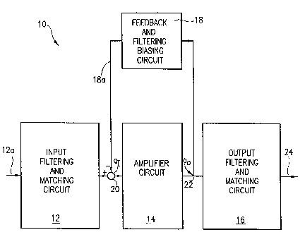
Figure 1 shows a block diagram of a class A/F amplifier
that is the subject matter of the present invention.
Figure 2 shows a more detailed block diagram of the class
A/F amplifier in Figure 1.
Figure 3 is a schematic of the class A/F amplifier shown
in Figures 1 and 2.
Figure 4 is a graph of spectral regrowth of a 5.5 watt
CDMA amplifier at 7 dB output power back-off.
-6-
CA 02248888 1998-10-15
REST MODE FOR CARRYING OUT THE INVENTION
Figure 1 shows an embodiment of an amp~ifier, which will
be referred to hereinafter as a class A/F amplifier, generally
indicated as l0.
The class A/F amplifier 10 has an input filtering and
matching circuit generally indicated as 12, an amplifier
circuit generally indicated as 14, an output filtering and
matching circuit generally indicated as 16, a feedback and
filtering biasing circuit generally indicated as 18, and a
first summing junction 20.
The input filtering and matching circuit 12 responds to a
radio frequency access signal along line 12a, for providing a
filtered and matched radio frequency access input signal. A
summing junction 20 responds to the filtered and matched radio
frequency access input signal, and further responds to a
feedback and filtered biasing signal along line 18a, for
providing a summed filtered, matched and feedback radio
frequency access input signal. The amplifying circuit 14
responds to the summed filtered, matched and feedback radio
frequency access input signal, for providing an amplified
filtered, matched and feedback radio frequency access input
signal to node 22. The feedback and filtering biasing circuit
17 responds to the amplified harmonically filtered radio
frequency input signal at node 20, for providing the feedback
and filtered biasing signal indicated as 18a. The output
filtering and matching circuit 16 responds to the amplified
filtered radio frequency access input signal indicated as 22,
CA 02248888 1998-10-15
for providing an amplified filtered and matched radio
frequency access output signal generally indicated as 24 to an
output circuit (not shown). The input and output filtering
may include a combination of one or more circuits for
distortion shunting, impedance matching or harmonic filtering,
all of which will be discussed in greater detail below.
The class A/F amplifier 10 is used in a mobile radio base
station (not shown) that receives the radio frequency access
input signal 18 from a mobile phone (not shown). The radio
frequency access input signal 18 may be either a frequency
division multiple access (FDMA) signal, a time division
multiple access (TDMA) signal, or a code division multiple
access (CDMA) signal.
Figure 2 shows a more detailed block diagram of the class
A/F amplifier in Figure 1. On the input side of the
amplifying circuit 14, the class A/F amplifier in Figure 2
includes the following: input distortion shunting circuits 38,
an input impedance matching circuit 40 and an input harmonic
filtering circuit 42. On the output side of the amplifying
circuit 14, the class A/F amplifier 10 in Figure 2 includes
the following: an output harmonic filtering circuit 44, an
output impedance matching circuit 46 and an output distortion
shunting circuit 48. The scope of the invention is not
intended to be limited to any particular kind of distortion
shunting, impedance matching or harmonic filtering circuits,
all of which will be discussed in greater detail below.
_g_
CA 02248888 1998-10-15
One important feature of the present invention is that
the radio frequency access input signal 18 is harmonically
filtered on both the input and output sides of the amplifying
circuit 14. The class A/F amplifier 10 in Figure 2 also has
an amplifier RF and DC bias filtering and feedback circuit 50
connecting the input side to the output side of the amplifying
circuit 14. The amplifier RF and DC bias filtering and
feedback circuit 50 corresponds to the filtering and feedback
biasing circuit 17 in Figure 1. The scope of the invention is
not intended to be limited to any particular kind of
amplifying, filtering or feedback circuit. The amplifying
circuit 14 will be discussed in greater detail below with
respect to Figure 3.
Figure 3 is a schematic of the class A/F amplifier 10 in
Figure 2. For the readers convenience, the summing junction
is shown as an amplifier input point ai in Figures 1 and 3
and the amplifier output point ao are also indicated in
Figures 1 and 3. In Figure 2, the input distortion shunting
and output distortion shunting circuits 38, 48 provide a low
20 pass harmonic short function to the input and output signals
of the class A/F amplifier 10. The input distortion shunting
circuit 38 and the output distortion shunting circuit 48 of
Figure 2 are respectively indicated as STUBIN plus gate CAPIN
and STUBOUT plus drain CAPOUT shown in Figure 3. The circuits
STUBIN and STUBOUT in Figure 3 include an inductor and a
capacitor connected in parallel to ground, not shown. The
scope of the invention is not intended to be limited to any
-9-
CA 02248888 1998-10-15
particular circuit design for the circuits STUBIN and STUBOUT
in Figure 3. For example, the inductor may be removed and the
cap replaced with an open stub.
The input and output impedance matching circuits 40, 46
in Figure 2 provide impedance matching for the class A/F
amplifier 10 with an input or output circuit connected thereto
(not shown). The input and output impedance matching circuit
40, 46 are generally indicated as INPTMCH and OUTPTMCH in
Figure 3. The impedance matching circuits INPTMCH and
OUTPTMCH include an inductor and a capacitor connected in
parallel, not shown, and coupled to the amplifying circuit 14.
The scope of the invention is not intended to be limited to
any particular circuit design for the impedance matching
circuits INPTMCH and OUTPTMCH in Figure 3.
The amplifying circuit 14 in Figure 2 includes a field
effect transistor (FET) generally indicated as TRANS in Figure
3, having a gate connection G, a drain connection D and a
source connection S. The scope of the invention is note
intended to be limited to any particular type of amplifying
circuit, transistor or FET transistor.
The input and output harmonic filtering circuits 42, 44
in Figure 2 provide input and output harmonic filtering of the
radio frequency access input signal before and after
amplification by the amplifier circuit 14. The input harmonic
filtering circuit 42 in Figure 2 includes a second order input
harmonic filtering circuit generally indicated as 2HARFLTIN in
Figure 3, and also includes a third order input harmonic
-10-
CA 02248888 1998-10-15
filtering circuit generally indicated as 3HARFLTIN also in
Figure 3. The second order input harmonic filtering circuit
2HARFLTIN in Figure 3 filters even harmonics from the radio
frequency access input signal. The third order input harmonic
filtering circuit 3HARFLTIN filters odd harmonics from the
radio frequency access input signal. In Figure 3, the second
order input harmonic filtering circuit 2HARFLTIN and the third
order input harmonic filtering circuit 3HARFLTIN may include a
bandstop filter that is tuned to eliminate the harmonics from
the radio frequency access input signal. The bandstop filter
also includes respective transmission lines, each having a
length of about 1/8 of the operating frequency wavelength or
an odd multiple thereof such as 3/8, 5/8 etc. and 1/12 of the
operating frequency wave or a multiple thereof such as 3/6,
5/8 etc., not generally including any multiple of 1/4 of the
operating frequency wavelength. Each field effect transistor
(FET) will have distinct 2nd and 3rd harmonic load impedances
required for best IMD supression. The load is tuned by
slightly changing the lengths of these lines. The lines are
also tuned to resonate out the even and odd has harmonies by
grounding them. The bandstop filter may include an inductor
and a capacitor connected in series (not shown) and coupled
between the gate G of the transistor TRANS to ground.
Similarly, the output harmonic filtering circuit 44 in
Figure 2 includes a second order input harmonic filtering
circuit generally indicated as 2HARFLTOUT in Figure 3, and
also includes a third order input harmonic filtering circuit
-11-
CA 02248888 1998-10-15
generally indicated as 3HARFLTOUT also in Figure 3. The
second order input harmonic filtering circuit 2HAR~LTOUT in
Figure 3 filters even harmonics from the amplified radio
frequency access input signal. The third order input harmonic
filtering circuit 3HARFLTOUT in Figure 3 filters odd harmonics
from the amplified radio frequency access input signal. In
Figure 3, the second order input harmonic filtering circuit
2HARFLTOUT and the third order input harmonic filtering
circuit 3HARFLTOUT may include a bandstop filter that is tuned
to eliminate the harmonics from the radio frequency access
input signal. The bandstop filter also has transmission lines
respectively having a length of about 1/8 of the operating
frequency wavelength or an odd multiple thereof such as 3/8,
5/8 etc. and 1/12 of the operating frequency wave or a
multiple thereof such as 3/6, 5/8 etc., not generally
including any multiple of 1/4 of the operating frequency
wavelength. As discussed above, each FET will have distinct
2nd and 3rd harmonic load impedances required for best IMD
supression. The is load is tuned by slightly changing the
lengths of these lines. The lines are tuned to resonate out
the even and odd has harmonies by grounding them. The
bandstop filter may include an inductor and a capacitor (not
shown) coupled between the drain D of the transistor TRAMS to
ground.
The input and output harmonic filtering circuits 42, 44
in Figure 2 may include a bias or harmonic filter cap circuit.
The filter cap circuit includes one or more capacitors
-12-
CA 02248888 1998-10-15
generally indicated as C1-C4 and C8-C11, one or more inductors
generally indicated as L1-L4 or one or more resistors R1
coupled to ground, all shown in Figure 3. These components in
the prior art functioned as bias caps. In the present
invention, these components perform optional filtering to
reduce IMD distortion in the input harmonic filtering network.
For example, in Figure 3 a capacitor C3 provides a filtering
cap for the second order input harmonic filtering circuit
2HARFLTIN, a capacitor C4 provides a filtering cap for the
third order input harmonic filtering circuit 3HARFLTIN, a
capacitor C9 provides a filtering cap for the second order
input harmonic filtering circuit 2HARFLTOUT, and a shuntstub
generally indicated as SHNTSTB, and capacitors C8, C8A provide
a filtering cap for the third order input harmonic filtering
circuit 3HARFLTOUT. In the third order input harmonic
filtering circuit 3HARFLTOUT, the shuntstub circuit SHNTSTB
and the capacitors C8, C8A when used together have produced
enhanced performance for the amplifier as a whole. The
shuntstub circuit SHNTSTB includes an inductor and a capacitor
connected in parallel to the output impedance matching circuit
46.
In Figure 3, capacitors generally indicated as CIN, COUT
provide a DC bypassing function on the input and output sides
of the class A/F amplifier 10.
As shown, the field effect transistor TRANS has the
feedback circuit or connection 50 between the drain D and the
gate 6 for suppressing oscillations in the class A/F
-13-
CA 02248888 1998-10-15
amplifier, that also includes a DC feedback resistor R2 to
minimize the effect of DC changes during ageing, a RF feedback
resistor R3 to minimize the effect of RF changes during
ageing, and a feedback bypass capacitor C6. The feedback is
adjusted to minimize self bias generated distortion, which
works in depletion mode devices. The scope of the invention
is not intended to be limited to embodiments having such a
feedback circuit or connection 50.
General Discussion of the Operation of the Amplifier
In operation, the class A/F amplifier of the present
invention encompasses the advantages of both the class A and
class F amplifiers combined and eliminates the disadvantages
thereof. Specifically, the class A/F amplifier of the present
invention uses a bias point halfway between the class A and F
amplifiers. Thus the class A/F amplifier is more efficient
than class A, and more linear than class F. The class A/F
amplifier has the high power gain of the class A amplifier and
also amplifies reduced power signals, while having the
harmonic filters of the class F amplifier, thus suppressing
IMD signals.
The most significant advantage of the present invention
is that the class A/F amplifier filters, when operated at a
class A bias, significantly reduce the intermodulation
distortion (IMD), which the class A amplifier normally cannot
suppress. The class A/F amplifier suppresses the IMD while
maximizing linear efficiency.
-14-
CA 02248888 1998-10-15
In a particular application for a mobile communication
system, such as a Personal Communication Service system, the
class A/F amplifier having the aforementioned novel matching
network has been shown to increase the CDMA power and linear
efficiency when compared to a class A amplifier. The simple,
inexpensive class F amplifier structure suppresses the 3rd and
5th order products more than 10 dB over the class A amplifier.
A 6.5 watt CDMA PCS class A/F amplifier demonstrated 20%
linear efficiency: a threefold improvement in linear
efficiency over typical PCS base station having the class A
amplifier. The 6.5 watt amplifier demonstrated a 2.7 times
improvement in linear power over a similar class A amplifier
(power matched but without the class F traps). The class A/F
amplifier improves linear power when compared to the class A
amplifier, by using a series of harmonic traps and filters,
while maintaining intersymbol interference levels through an
intrinsic cosine filter. Linearity is not degraded by unequal
power tones as in the class A/B amplifiers.
In effect, the class A/F amplifier of the present
invention uses four similar filters on the input and the
output as well, as shown in Figure 3. The filter next to the
transistor TRAMS is a single pole shunt capacitor, which is
labeled gate capacitor CAPIN on the input and drain capacitor
CAPOUT on the output. The capacitors gate CAPIN and drain
CAPOUT plus the intrinsic inductance of the transistor TRAMS
act as low pass filters, and slightly round the output from
pulse to pulse which suppresses the spectral regrowth. These
-15-
CA 02248888 1998-10-15
capacitors also are used with the feedback to adjust the
amount of self biasing. The next filter is a pair of series
tanks to ground, which consist of a short piece of
transmission line ended with a cap shorted to ground. One
series filter resonates (minimizes) the even harmonics which
is labeled 2HARFLTIN (input), and 2HARFLTOUT (output) and the
other filter resonates (minimizes) the odd harmonics which are
labeled 3HARFLTIN (input), and 3HARFLTOUT (output). As
discussed above, if the harmonics are suppressed then the
intermodulation components will also be suppressed. The last
and final filter/matching network is a series quarter-wave-
line at the third harmonic followed by open stubs, which are
labeled STUBIN and STUBOUT. The final filter/matching network
acts as a third harmonic short.
One selection criteria for the transistor is to pick one
that has the highest linear efficiency. This can be
accomplished by load pulling transistors under two-tone drive
conditions to determine which has the greatest linear
efficiency. In practice, a number of transistors were tested
and Lateral Drain Metal Oxide Semiconductor (LDMOS)
transistors were selected and measured. Bipolar Junction
Transistors (BJT) achieve around 5% efficiency at 40 dB
carrier to IM3 ratios (i.e. 3rd Order Intermodulation
Products). In comparison, LDMOS transistors, when operating
the class A/F amplifier, achieve nearly 20% efficiency at
similar IMD ratios.
-16-
CA 02248888 1998-10-15
A single stage LDMOS class A/F amplifier was tested.
While operating with the class F components removed and with
power matching, the single stage LDMOS class A/F amplifier
operated at IS-97 linearity levels of 2.4 watts. When
operating with the class F network attached, the single stage
LDMOS class A/F amplifier produced 5.5 watts of linear IS-97
power levels as shown in Figure 8. Noise levels (CDMA spec
levels) of the amplifiers were compared. The class A/F
amplifier did not increase the noise floor. Both amplifiers
were operated at the same bias power of 37 watts. Therefore,
the class A efficiency was 6.4%, while the class A/F
efficiency was 17.3%.
In summary, the class A/F amplification provides improved
linear efficiency when compared to class A and class AB
amplifiers. A three fold improvement in linear efficiency was
found, which was accomplished by reducing the second and third
harmonics through use of class F traps.
The class A/F amplifier of the present invention is also
an important contribution to the state of the art for other
reasons: It has been shown that CDMA (a common spread
spectrum signal) is a noise-like signal immune at a minimum of
dB to spurious non spread-spectrum signals. The CDMA is
also susceptible to its own spectral regrowth interference,
which limits the system capacity. Thus, for PCS CDMA systems
25 to operate most cost effectively, inexpensive linear power
amplifiers are required. Power amplifier linearity is
determined by transistor performance and signal parameters.
-17-
CA 02248888 1998-10-15
First, transistor performance parameters such as gate
rectification or nonlinear variation of transistor charge are
significant causes of nonlinearity. Second, CDMA signals have
reduced linearity for multiple reasons: Commercial PCS systems
operate under wideband-width BPSK-DS-SS modulation at a high
modulation rate with a two sigma statistical peak of 6 dB peak
to average ratio. Then if one analyzes the harmonics of
multitone signals to determine the power coefficients, i.e.
using the MacLaurin case of the Taylor series, one sees that
the harmonics and their associated intermodulation components
can be quite strong which results in intersymbol interference
and the associated BER degradation limiting the capacity of
the PCS CDMA wireless system.
In addition to linearity, power added efficiency is a
critical parameter because of the heat generation. In the
past heat generation was not a problem. However, more
recently the public is increasingly resisting the addition of
large tower sites. This forces more creative placement of PCS
base stations. This space restriction resulted in
requirements for less heat generation. This heat also affects
reliability. Hot amplifiers have low reliability.
Background Analysis of the Overall Performance
Background analysis of the overall performance of the
class A/F of the present invention is briefly discussed below:
One can mathematically analyze the significance of the
harmonics through use of a Taylor series of two tones.
-18-
CA 02248888 1998-10-15
Through measurements we found that the harmonic and
intermodulation products from a saturated amplifier
approximately followed a tanh function. To calculate these
products one calculates the first to third order derivatives
of the tanh function. It was found the Taylor series
coefficients to be 0 for the DC term, 1 for the fl term, 0 for
the f2 term and -1/3 for the f3 term by solving the equation:
y~~ _ { [A(sin(wlt) + sin(wzt) ) - .33A3{1 - cos(2Wlt) ) /2 +
(1-cos(2WZt) ) /2 + [cos(w,-w2)t -
to cos (w1+w2) t} {sin (w,t) + sin (wZt) } ]2} /50
The powers (summed Taylor coefficients) of each carrier
are determined to be (A2)/50 and each of the third order
products are determined to be (((A3)/4)2)/50. These
coefficients (and further measurements) show that at saturated
output power the third order distortion products will be 12 dB
down below the carrier. Shorting out the harmonic
mathematically removes the 2f2-fi term and the 2f1-f2 term.
Measurements show that the terms are reduced more than 20 dB.
When implemented these networks allow the transistor to be
operated much closer to saturation than a non-class F
transistor. The CDMA amplifiers have a 15 dB peak to average
ratio. To obtain the needed linearity the amplifiers output
power was backed-off 7 dB, when compared to the typically
required il dB back-off from a bipolar junction transistor.
Thus the class A/F amplifier is backed off only 7 dB while
-19-
CA 02248888 1998-10-15
operated at the bias of a class A amplifier backed off 11 dB.
Therefore, the class A/F amplifier has 4 dB more output power
than the class A amplifier at the same linearity, with an
associated improvement in efficiency.
To remove the harmonics, the class F amplifier is used.
A class F amplifier is a class B amplifier which has
additional harmonic-suppression-networks for development of a
squarer wave form which improves efficiency, as shown in
Figure 4. The class A/F amplifier when operated at its most
efficient point is not very linear. But when backed off the
class A/F amplifier is more linear and efficient than the
class A amplifier. The industry custom is to use a class A/B
amplifier to amplify the signal. When one biases the class
A/B amplifier, it is more linear and efficient with a pair of
equal tones than the class A amplifier. But, when the tones
are not of equal strength, the class A/B amplifier is self
biased by the higher of the two tones which suppresses and
distorts the lower of the two tones. The class A/B amplifier
acts like a limited filter which distorts lower power signals
and in the process generates higher noise power. A recent
measurement found the noise floor of the class A/B amplifier
increased by 6 dB. This increased noise power acts as an
interference which significantly reduces the wireless systems
range and capacity. Thus the class A/B amplifier increased
the amplifier efficiency at the cost of link efficiency.
-20-
CA 02248888 1998-10-15
Components List For Schematic Figure 3
Component Function
CIN, COUT DC bypassing capacitors
C1-C4, C8-C11
Filter capacitors
CAPIN Gate capacitor for gain adjust, self bias
control, harmonic supression
CAPOUT Drain capacitor for gain adjust, self bias
control, harmonic supression
C6 Feedback bypassing capacitor
R2 DC feedback resistor that minimizes device DC
changes during aging and sets device self-bias
for maximizing linearity
R3 RF feedback resistor that minimizes device RF
changes during aging and minimizes Rf generated
self biasing
TRANS Motorola LDMOS transistor (although approach
will work with any field effect transistor)
STUBIN Class A/F lowpass filter odd harmonic short
STUBOUT Class A/F lowpass filter odd harmonic short
2HARFLTIN Class A/F bandstop filter even harmonics in
3HARFLTIN Class A/F bandstop filter odd harmonics in
2HARFLTOUT Class A/F bandstop filter even harmonics out
3HARFLTOUT Class A/F bandstop filter odd harmonics out
-21-
CA 02248888 1998-10-15
General Reference Guide
Some other general references in the field include: T.S.
Rappaport, Wireless Communications Principles & Practice,
Prentice Hall PTR, Upper Saddle River, New Jersey, 1996; L.W.
Couch II, Analog and Digital Communication Systems, Macmillin
Pub. Company, New York, 1987; Wu et al., "Linear RF Power
Amplifier Design for CDMA Signals", IEEE MTT-S Digest, 1996,
Page 851; and R. S. Brozovich, D. R. Helms et al. "Highly-
Linear Highly-Efficient HBT for Communications Circuits." GaAs
IC, 1994, page 291.
Scope of the Invention
Although the present invention has been described and
discussed herein with respect to at least one embodiment,
other arrangements or configurations may also be used that do
not depart from the spirit and scope of the invention.
For example, the scope of the invention is not intended
to be limited to any particular capacitance, inductance or
resistance shown in Figure 3.
Moreover, the scope of the invention is not intended to
be limited to an amplifier for amplifying only a radio
frequency access input signal, like the frequency division
multiple access (FDMA) signal, the time division multiple
access (TDMA) signal, or the code division multiple access
(CDMA) signal. The thrust of the invention relates to
harmonic filtering of any signal before and after
amplification. For instance, embodiments are envisioned
-22-
CA 02248888 1998-10-15
wherein the amplifier is a class A/F amplifier having a
harmonic filtering circuit that responds to any input signal,
for providing a harmonically filtered input signal, and
further responds to an amplified harmonically filtered input
signal, for providing any amplified harmonically filtered
output signal.
The class A/F amplifier has an amplifying circuit that
responds to the harmonically filtered input signal, for
providing the amplified harmonically filtered input signal.
The harmonic filtering circuit also has an input harmonic
filtering circuit for filtering harmonics from the input
signal, and output harmonic filtering circuit for filtering
harmonics from the amplified harmonically filtered input
signal. (The input filtering removes transistor generated
distortion.)
The input harmonic filtering circuit has a second order
input harmonic filtering circuit for filtering even harmonics
from the input signal, and a third order input harmonic
filtering circuit for filtering odd harmonics from the input
signal.
The output harmonic filtering circuit has a second order
output harmonic filtering circuit for filtering even harmonics
from the amplified harmonically filtered input signal, and a
third order output harmonic filtering circuit for filtering
odd harmonics from the amplified harmonically filtered input
signal.
-23-