Language selection

Search

Patent 2249398 Summary

Third-party information liability

Some of the information on this Web page has been provided by external sources. The Government of Canada is not responsible for the accuracy, reliability or currency of the information supplied by external sources. Users wishing to rely upon this information should consult directly with the source of the information. Content provided by external sources is not subject to official languages, privacy and accessibility requirements.

Claims and Abstract availability

Any discrepancies in the text and image of the Claims and Abstract are due to differing posting times. Text of the Claims and Abstract are posted:

  • At the time the application is open to public inspection;
  • At the time of issue of the patent (grant).
(12) Patent: (11) CA 2249398
(54) English Title: METHOD FOR THE MANUFACTURE OF LASERS WITH TAPERED GUIDE REGION
(54) French Title: PROCEDE DE FABRICATION DE LASERS A GUIDE EN BISEAU
Status: Expired and beyond the Period of Reversal
Bibliographic Data
(51) International Patent Classification (IPC):
  • G02B 6/12 (2006.01)
  • G02B 6/122 (2006.01)
(72) Inventors :
  • FANG, RUIYU (Italy)
(73) Owners :
  • AVAGO TECHNOLOGIES GENERAL IP (SINGAPORE) PTE. LTD.
(71) Applicants :
  • AVAGO TECHNOLOGIES GENERAL IP (SINGAPORE) PTE. LTD. (Singapore)
(74) Agent: SMART & BIGGAR LP
(74) Associate agent:
(45) Issued: 2001-06-12
(86) PCT Filing Date: 1997-03-19
(87) Open to Public Inspection: 1997-10-02
Examination requested: 1998-09-21
Availability of licence: N/A
Dedicated to the Public: N/A
(25) Language of filing: English

Patent Cooperation Treaty (PCT): Yes
(86) PCT Filing Number: PCT/EP1997/001385
(87) International Publication Number: WO 1997036353
(85) National Entry: 1998-09-21

(30) Application Priority Data:
Application No. Country/Territory Date
TO96A000219 (Italy) 1996-03-22

Abstracts

English Abstract


The laterally tapered active region (3, 3a) is obtained by means of
photolithography techniques, in two successive steps, by overlaying the images
of a first and a second mask (5, 6) each presenting a chamfer whose
inclination corresponds to the inclination of one of the sides of the tapered
region (3a).


French Abstract

On obtient une région active biseautée (3, 3a) à l'aide de techniques de photolithographie, en deux étapes successives, en superposant les images d'un premier et d'un second masque (5, 6) dont chacune présente un chanfrein dont l'inclinaison correspond à celle de l'un des côtés de la partie en biseau (3a).

Claims

Note: Claims are shown in the official language in which they were submitted.

Claim
Method for the manufacture of solid state lasers comprising an active region
(3) ending in a laterally tapered region (3a), characterised in that said tapered region
(3a) is obtained by means of photolithography techniques, in two successive steps,
by images respectively of a first and of a second mask (5, 6) each with a chamfer
whose inclination corresponds with the inclination of one of the sides of the tapered
region (3a), and in that in the second step the second mask (6) is partially overlaid
on the image (9) of the first mask (5), so that the second image overlaps the first in
an area whose shape and size correspond with those of the tapered region (3a).

Description

Note: Descriptions are shown in the official language in which they were submitted.


CA 02249398 1998-09-21
WO 97/36353 PCTIEP97/01385
-
U!ETHOD FOR THE MANUFACTURE OF LASERS WITH TAPERED GUIDE REGION
The invention described herein relates lo components for optical communications
systems and in particular it conc~.~-s a method for the manufacture of a solid state laser with
laterally tapered guide region.
In oDtical cornmunicatiOns systems it is often nec~.y to couple a solid state laser
with an optical w 1,~ jV 'e One of the ~ E..ls encountered in this cou,~ .y is given by the
limited gOG~ tli-, t~l ..nces allowed for co"~ctly positioni..g the laser er..ission region with
respect to the guide, bec?n~~ of the reduced size of the regions i~olv_d. On the contrary,
1() a wide positior.ins~ tolerance is an .n~ollal~t prere~uisite for the future ar~lic~ ions of
integrated o,oto ele_lr..nic devices in optical commu..i: ,t ~ns systems.
In order to reach this goal, it has recently been ~uyosed to taper the active layer of the
laser: such laper;--g makes the effective refractive index of the active layer become close to
that of the material making up the ad~ac~ril layers and this guarantees increased power
1~ t.ansfer to the fibre. Fxamples of tapered lasers are described, for i.. stance, in the papers
"L~erally Tapered InP-lnGaAsP Waveguides for Low-Loss Chip-to-Fiber Butt Coupling: A
Comparison of Different Configurations" by R. Zengerle et al., IEEE Photonics Technology
Letters, Vol. 7, No. 5, May 1995, and "InGaAsP/lnP tapered active layer multiquantum well
laser with 1.8 dB coupling loss to cleaved single mode fibre", by l.F. Lealman et al., Elec-
2n tronics Letters, 29 September 1994, Vol. 30, No. 20.
A problem encountered in manufacturing tapered guides is that, to obtain -s~ to,y
p~ . f.n,.ance, the narrow end of the taPered region must have a very small width, on the order
of 0.1 - 0.2 ~m. To obtain sizes of this order of magnitude, manufacturers employ eleclron
beam writing techniques, as indicated in particular in the article by R. Zengerle mentioned
above.
The use of this type of techni~ue has several J, ~ Lac,ks. First, the operation is long
and the equipment required is very ex~ensive, and this makes finished devices very expensi-
ve. Moreover, since electrically charged particles are used, the techri~ e can be emploved

CA 02249398 1998-09-21
W O 97/36353 PCT~EP97101385
without difficulties onty to make ~uides on materials with a certain degree of electrical
conductivity, such as semiconductors. It can be employed with many difficulties when the
auides are realised on films made of insulating materials ~such as SiN~), which are em-
ployed for the manufacture of certain co~ G,-ents: in this case, an accumulation of
charges would quickly build u~, thus preventing the successful cor,~plEtion of the
operation.
According to the present invention, a method is instead provided wherein the
ta~-ered region of the active layer is obtained without the use of costly equipment and
without employing electrically charged pal licles, so that the method can also be used
lf) without any problem for insulating materials as well.
The method is characterised in that the active layer is ta~ered by means of
photolill,oy.aphy techni~ues, in two successive steps, by fGr---i.-g images respective-
ly of a tirst and of a second mask each presenting a cha,..fer with an inclination
co~,espG,-ding to the irlclilldtion of one of the sides of the ta,oered region, and in that
1~ in the second step the second mask is partially overlaid on the image of the first
mask, so that the second image overlaps the first in an area whose shape and size
correspond with those of the tapered region.
For the sake of better clar~ty, lefere.-ce is made to the enclosed drawings,
wherein:
~1 - Figures 1, 2 are a perspective and a cross-section schematic represe"talion of a
laser with tapered active region;
- Figure 3 is a top view of the active region;
- Figures 4, 5 show an enlarge.ne.~t of the masks to be used to form the tapered region; and
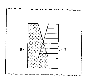
- Figure 6 is a top view pertaining to a step of the process to form the tapered region.
As can be seen in Figures 1 - 3, a semiconductor laser with tapered guide
region comprises a substrate 1 made of a suitable material (for inst,..)ce InP~ on
which a buffer layer 2 (made of InP with n-type doping), active layer 3 ~made of an
:~!! InGaAsP quaternary alloy) and cover layer 4, ag~in made of InP, are deposited. The
actlve layer is in the form of a stri~ with a tapered end portion 3a, as can clearly be
seen in Figure 3.
-~ It should be specified that the tapered guide could be made either directly on
the semiconductor material, or on a film of insulating material such as SiN4, asrequired for other laser structures.

CA 02249398 l998-09-2l
W O 97/36353 PCTAEP97/01385
According to the invention, the tapered region is obtained through a photo-
lithography process in two steps, and one side of the taper is realised during each
step. In the two steps, the masks depicted in Figures 4 and 5 are respectively used.
The masks, formed for example on glass, have each two opaque regions 5,
ô and respectively 7, 8.
The first region 5 (Figure 4) or respectively 7 (Figure 5) is shaped essentiallylike a rectangular trapezoid (or has at least an end part sha"ed like a rectangular
l,apezoid), whose oblique side has the profile and inclination corresponding with
those desired for active region taper- In general, the profile of taper 3a (Figure 3) will
be rectilinear, although also curvilinea~ tapers could be formed. Regions 5 and 7 on
the two masks esse.-lially mirror each other. Note that, though for the sake of
simplicity the oblique side of the lra;~ezoidal regions cf the masks is depicted as a
continuous profile, in reality it will comprise a series of steps, of extremely small
pitch, as the techniques for the realisation of the masks do not allow forming
l~ continuous profiles. Typical sizes for the two sides of the trapezoidal region shall be
on the order of 1-1.5 micron for the minor base and 3 micron for the major base. The
length of the oblique side will depend on the required taper angle.
The second region 6 (Figure 4) or respectively 8 ~Figure 5) is an essentially
rectangular region co,,stilLIting a conventional r~ference or marker for the correct
positioning of the mask during the fal~rication ~rocess.
To fal,ricate the laser, the various layers are formed in a wholly conventional
manner. Atter forming the active layer essentially on the entire buffer layer, the
images of region 5 (indicated by 9 in Figure 6) and of marker 6 are formed with
con~erlional ~hotolithography techniques. The same o~,erdtions are then repeatedwith the second mask, by overlaying region 7 to image 9, so that the overlap area
reproduces the shape o~ ~uide 3, as can be seen in Figure 6. At the end of the
second step, after the ~.I,otose.-sili~/e material is removed, the active layer is actually
reduced to just tapered layer guide 3. The laser is then completed in a wholly
conve.,lional manner.
~n It is evident that, thanks to the manufacture of the guide in two steps, and
~herefore to the use of two masks, pr~L,lem~s stemming from the small size of the tip
Gf the guide are eliminated: the tip is actually obtained as the intersection af the
~ edges of two images and the definition currently achievable with photolithography
techniques allows obtainin~ the sizes mentioned above without any problems.
To obtain the tapered guide, accurate mask positioning is important. for this

CA 02249398 1998-09-21
W O 97/36353 PCT~EP97/0138~ -
purpose, as has been stated above, the masks are provided with a reference marker
6 or respectively 8, placed at a ple-set distance from a longitudinal axis of the
~rapezoidal region (e.g. an axis dividing the minor base in half). Note that develop-
ment results in an image whose size is slightly reduced with respect to those of the
mask, to an extent depending on the particular photo-resist and on the photo-
lilhog~d~ y co-.ditiu--s employed: lher~f~-e, both region 7 and marker 8 in the second
mask shall have slightly smaller sizes than those of the first mask. Moreover, it will
be necessary to take care that the side of marker 8 closer to region 7 is actually at
the pre-set distance from the aforesaid longitudinal axis.
n ~t is evident that what has been described a~ove is ,. -ovicJed purely by way
of non-limiting example and that variations and modifications are possible without
departing from the scope of the invention.

Representative Drawing
A single figure which represents the drawing illustrating the invention.
Administrative Status

2024-08-01:As part of the Next Generation Patents (NGP) transition, the Canadian Patents Database (CPD) now contains a more detailed Event History, which replicates the Event Log of our new back-office solution.

Please note that "Inactive:" events refers to events no longer in use in our new back-office solution.

For a clearer understanding of the status of the application/patent presented on this page, the site Disclaimer , as well as the definitions for Patent , Event History , Maintenance Fee  and Payment History  should be consulted.

Event History

Description Date
Inactive: IPC deactivated 2011-07-29
Time Limit for Reversal Expired 2009-03-19
Letter Sent 2008-03-19
Letter Sent 2007-09-20
Inactive: IPC from MCD 2006-03-12
Inactive: First IPC derived 2006-03-12
Inactive: IPC from MCD 2006-03-12
Grant by Issuance 2001-06-12
Inactive: Cover page published 2001-06-11
Letter Sent 2001-06-07
Inactive: Final fee received 2001-03-12
Pre-grant 2001-03-12
Letter Sent 2001-01-02
Notice of Allowance is Issued 2001-01-02
Inactive: Approved for allowance (AFA) 2000-12-07
Letter Sent 2000-05-12
Inactive: Multiple transfers 2000-04-11
Inactive: IPC assigned 1998-12-01
Classification Modified 1998-12-01
Inactive: First IPC assigned 1998-12-01
Inactive: Acknowledgment of national entry - RFE 1998-11-17
Application Received - PCT 1998-11-13
All Requirements for Examination Determined Compliant 1998-09-21
Request for Examination Requirements Determined Compliant 1998-09-21
Application Published (Open to Public Inspection) 1997-10-02

Abandonment History

There is no abandonment history.

Maintenance Fee

The last payment was received on 2001-03-05

Note : If the full payment has not been received on or before the date indicated, a further fee may be required which may be one of the following

  • the reinstatement fee;
  • the late payment fee; or
  • additional fee to reverse deemed expiry.

Please refer to the CIPO Patent Fees web page to see all current fee amounts.

Owners on Record

Note: Records showing the ownership history in alphabetical order.

Current Owners on Record
AVAGO TECHNOLOGIES GENERAL IP (SINGAPORE) PTE. LTD.
Past Owners on Record
RUIYU FANG
Past Owners that do not appear in the "Owners on Record" listing will appear in other documentation within the application.
Documents

To view selected files, please enter reCAPTCHA code :


To view images, click a link in the Document Description column. To download the documents, select one or more checkboxes in the first column and then click the "Download Selected in PDF format (Zip Archive)" or the "Download Selected as Single PDF" button.

List of published and non-published patent-specific documents on the CPD .

If you have any difficulty accessing content, you can call the Client Service Centre at 1-866-997-1936 or send them an e-mail at CIPO Client Service Centre.


Document
Description 
Date
(yyyy-mm-dd) 
Number of pages   Size of Image (KB) 
Abstract 1998-09-21 1 40
Description 1998-09-21 4 180
Claims 1998-09-21 1 17
Drawings 1998-09-21 2 29
Cover Page 1998-12-07 1 32
Cover Page 2001-05-10 1 26
Representative drawing 1998-12-07 1 5
Representative drawing 2001-05-10 1 6
Reminder of maintenance fee due 1998-11-23 1 110
Notice of National Entry 1998-11-17 1 201
Courtesy - Certificate of registration (related document(s)) 1998-11-17 1 114
Commissioner's Notice - Application Found Allowable 2001-01-02 1 165
Maintenance Fee Notice 2008-04-30 1 172
PCT 1998-09-21 11 313
Correspondence 2000-05-12 1 23
Correspondence 2001-03-12 1 46
Fees 2001-03-05 1 31
Fees 1999-02-24 1 27
Fees 2000-02-16 1 30