Note: Descriptions are shown in the official language in which they were submitted.
CA 022~0020 1998-09-24
Method and Device for the electrochemical Treatment with Treatment Liquid of
an Item to be treated.
Specification
The invention relates to a method for the electrochemical treatment of an item to be
treated with treatment liquid and also to a device for carrying out the procedure.
In order to produce circuit boards, conductive structures, the conductor lines, must
be formed on their surfaces. The latter represent mutually insulated islands which
can be treated selectively.
The structures on the item to be treated, for example on circuit boards, must have,
however, an electrically conductive connection respectively to the bath current
source during treatment since electrochemical treatment of an item to be treatedfundamentally presupposes that the surfaces to be treated are electrically
conductive. In known electrochemical methods for treating structures on circuit
boards therefore, a completely electroplated and, if necessary, through hole plated
circuit board which is electrolytically reinforced with copper is assumed. The
structures are deposited onto the circuit boards, which are so prepared, by printing
or in a photographic manner, for example, with a negative image of the structure.
Subsequently, the non-masked, electrically conductive surfaces are treated
electrochemically in a selective manner. As a rule, several procedural steps arerequired here. Finally, the electrically conductive layer between the structures must
be completely removed by etching. The etching process is performed preferably inchemical baths using splashing and spraying techniques.
A disadvantage in this procedure is that the item to be treated must be placed twice
into a wet-chemical treatment production line: firstly, the circuit boards are through
hole plated. Then, the boards are printed with the structure image outwith the wet
area and subsequently they are inserted once again into a wet-chemical treatmentproduction line for treating the structures. Corresponding rinsing and drying
processes are necessary. Furthermore, it is disadvantageous that the conductive
base layer between the structures cannot be removed until the conductor lines have
been manufactured. For this purpose, the surfaces of the conductor lines must be
CA 022~0020 1998-09-24
provided with additional protection so that they are not damaged during the etching
process.
The same is true for the production of inner layers of multi-layer courses. In order to
prevent two-fold insertion into the wet-chemical treatment production lines
(electrochemical all-over treatment of the surface, removal, printing and
subsequently further treatment with wet-chemical methods), the untreated holohedral
copper surfaces can also be printed first. Then the etching process and the further
selective surface treatment can be carried out in a chemical manner. The remaining
copper surfaces, which represent electrically insulated islands after etching, are
oxidised brown or black in order to improve the adhesion while pressing several
inner layers of this type by known methods onto the surfaces. Subsequently, the
surfaces are chemically reduced to improve the corrosion properties. These
chemical processes are time-consuming and very expensive as a consequence of a
continual high consumption of chemicals and the disposal of large amounts of spent
chemicals. In contrast, the electrochemical processes for oxidisation or reduction of
the copper surfaces have considerable advantages when compared to purely
chemical treatment.
In the publication DE 43 37 988 A1, a method for producing multi-layer inner layers
is described. It is suggested here, that the oxidised copper surfaces be
electrochemically reduced in a horizontal through-put unit. A salt solution, forexample, should be used as an electrolyte. The oxidised surfaces are electrically
contacted with cathodic polarity via one or two pairs of rollers per multi-layer layer,
while the structures are joined electrically to the bath current source via the rollers.
The anodes are arranged in such a way that the item to be treated can be directed
through between the latter. By means of electrolysis, hydrogen in atomic form,
which reduces the copper oxide, appears at the cathodically polarised surfaces of
the item. The cost hereby is small in comparison to chemical reduction.
The disadvantage in this procedure is that the contact time on the rollers during the
through-put is very small. A conductor line or an insulated land for soldering with a
measurement of one millimetre is contacted in the direction of transportation of the
CA 022C70020 1998-09-24
_ .
circuit boards only for a very short spell of about 0.06 seconds at a transportation
speed of 1 m/min. This short time span is however far too small for electrochemical
treatment. Other conductor lines on the circuit membrane which are aligned parallel
to the direction of transportation have, in accordance with their length, an essentially
longer contact time. The result is that the effective treatment time is dependent upon
the alignment of the structures on the item to be treated. Furthermore, it is
disadvantageous that the contact rollers must be constructed very precisely to be
able to contact all the mutually insulated copper surfaces along the surface line and
hence to treat them. With a cathodic connection of the rollers furthermore, the latter
are inclined to collect impurities which adhere in part very firmly. Consequently, the
uniform contacting of the item to be treated is further hampered. If an electroplating
process is~the electrochemical procedure used here, the rollers are likewise very
strongly electroplated so that a continuous operation is not possible using thismethod.
The roller contact is then also fundamentally inappropriate if the structures are to be
only partially electrochemically treated. In this case, the surfaces which are not to be
treated are masked with a solder resist. Then, the deeper Iying surfaces to be
treated cannot be reached by the contact rollers.
Another method and a device suitable therefor is known from US-A 51 14 558. In
this publication a device is described for producing fine conductor lines on circuit
boards at a small spacing from one another. This device contains, in an
embodiment for contacting conductor lines, a multiplicity of brush fibres which are
arranged in two planes and which abut on both sides of the circuit boards at a
vertical orientation to the direction of transportation. These brushes are connected
to a current source and are polarised anodically during etching of the structures from
dead flat laminate. A counter-electrode is provided on the other side of the brush
arrangement, as seen from the plane of the circuit board, which is likewise
connected to a current source and cathodically polarised in the shown arrangement.
However, this device is not suited to performing an electrochemical treatment of the
electroplated surfaces on the circuit boards with sufficiently high currents since the
counter-electrode is completely screened by the brushes. It can even be supposed
~_ ... , .. ~ . . . ..
CA 022~0020 1998-09-24
..
that, with this arrangement, absolutely no electric current can be produced on the
circuit boards. It is rather the case that all the electrochemical processes take place
within a gap between the counter-electrodes and the brushes.
In the further publication, DE 41 23 985 C2, a device is presented for the electrolytic
treatment of circuit boards especially for the electrolytic treatment with copper. In
order to solve the problem described there that normally electrolytically deposited
metai is formed at the contact point to the circuit boards, it is likewise proposed that
brushes be used for contacting the circuit boards. These brushes are installed at the
edge of the circuit board surfaces to form an electrical contact between the current
source and the circuit board, which had been coated with dead-flat metal layers.Certainly, the possibility does not exist either with this device of contacting
electroplated areas of the circuit board surface, which are insulated from one another
electrically.
Therefore, the problem underlying the present invention is to avoid thedisadvantages of the state of the art and in particular to provide an appropriate
method and a device for the electrochemical treatment of areas, which are mutually
electrically insulated and electrically conductive, on an item to be treated, especially
on circuit boards by means of treatment liquid. Above all, the method and deviceshould be suited to treating circuit boards in through-put units in which the circuit
boards are maintained in a horizontal or vertical position and to making possible a
treatment of structures, which consist of very small insulated surfaces, and/or only a
partial treatment of electrically conductive structures. An essential aspect of the
invention concerns in addition the problem that, onto the contact elements in
electrolytic metal deposition, metal is also deposited on the contact elements so that
suitable measures need to be adopted to resolve this problem also.
These problems are resolved by the subject of Claims 1 and 10. Preferred
embodiments of the invention are presented in the sub-Claims.
With the method according to the invention and the device, an item to be treated can
be conveyed on a transportation track through the device by means of appropriate
CA 02250020 1998-09-24
.
transportation devices. Furthermore, further appropriate devices are provided for
guiding or containing the treatment liquid which are arranged in such a way that the
item, when being conveyed through the device, is brought into contact at least
temporarily with the treatment liquid, for example by submerging or soaking. All the
mutually electrically insulated and electrically conductive areas on the item to be
treated, for example the circuit boards, are brought into contact with stationary brush
electrodes, which are supplied from a current source via electrical connections, at
least one after another so that an electric potential abuts the areas while the areas
are in contact with the treatment liquid. Furthermore, counter-electrodes are
provided which are likewise arranged near the transportation track and which aresupplied from a current source via electrical connections with reversed polarity and
are arrang-ed in such a way that an electric current can flow between the areas and
the counter-electrodes. As a result, it is guaranteed that all electrically conductive
areas are treated electrochemically one after another with simultaneous contact with
the liquid treatment means. It is also possible with the method and device to treat
very small electrically conductive areas only partially. Furthermore, with the
electrochemical treatment on the brush electrodes, deposited metal can be cleared
again from settled metal.
A preferred application of the method according to the invention or a preferred
embodiment of the device consists in treating the circuit boards in a continuousmanner in a through-put unit. For this purpose, the boards are conveyed through the
unit in a horizontal direction of movement by means of appropriate transportation
devices, for example rollers or wheels and proceed thereby for example into a bath
of treatment liquid or are soaked or sprayed by appropriate devices. The circuitboards can thereby be orientated horizontally or vertically. The brush electrodes and
counter-electrodes for the electrochemical treatment are situated preferably on both
sides of the transportation track, i.e. for example, above and below the plane of
movement. The boards are therefore conveyed through between the electrodes. Of
course, the electrodes can also be arranged exclusively on one side of the circuit
boards. In order to achieve an optimal distribution of electrical field lines in the
space between the electrodes and the transportation track, the brush electrodes and
the counter-electrodes are arranged preferably alternately near the transportation
. , . . -- . ,
CA 022~0020 1998-09-24
track seen from the direction of transportation or another direction so that thecounter-electrodes are arranged between the brush electrodes which are arranged
adjacent to one another on one side of the item to be treated.
The brushes consist of fine-strand, electrically conductive fibres. They are arranged
preferably within the treatment liquid below the bath liquid level and are constructed
preferably in the form of rows which are aligned parallel to one another. These rows
can be arranged at an angle greater than zero to the direction of transportation of the
item to be treated, preferably perpendicular to the direction of transportation and
parallel to the transportation track which is constructed preferably in the form of a
plane of transportation.
i
For protection against chemical and electrochemical attacks the brushes consist of
resistant materials such as, for example, titanium, niobium, tantalum, noble metals or
special steel. The fibres of the brushes, for example with a fibre diameter of 0.01
mm are very elastic. They are very well suited to the surface to be treated. This
also makes possible the partial treatment of structures, which lie deeper than the
insulating layers near these areas (for example near a solder resist). The fibrebunches reach even the smallest surface regions between these insulations. The
fine-strand fibres do not cause any damage to the surfaces to be treated because of
their elasticity. In conjunction with a large number of fibres per brush, a long contact
time of the individual structures is achieved with a corresponding arrangement of
many brushes transversely to the direction of transportation of the item to be treated.
The electrochemical treatment is also correspondingly long. In electrochemical
processes, in which no metal is deposited, the contact time can be almost 100 per
cent because the counter-electrodes can be arranged right beside the brushes. This
implies that each insulated structure constantly remains in electrical contact with the
bath current source while proceeding through the electrochemical bath despite the
spacings of the brush electrodes from one another which is caused by the counter-
electrodes. Electrochemical processes of this type are for example electrolytic
cleaning, oxidisation, reduction and etching (engraving). Depending on the method
used, the brushes and, via the latter, the item to be treated are polarised anodically
or cathodically.
CA 022~0020 1998-09-24
The method according to the invention is also particularly suited to those
electrochemical processes in which metals are being deposited on the item to be
treated. Examples of this are the selective deposition of copper, gold, nickel, tin and
also tin/lead-, copper/tin- and copper/zinc alloys on structured circuit boards.Furthermore the method and device are also suited to the fully additive production of
circuit boards by electrochemical metal deposition, especially by copper deposition.
In electrolytic metal deposition, the brush electrodes are connected cathodically.
This means that the electrically non-insulated surface regions of the brushes, as well
as the item to be treated, become electroplated. Therefore, from time to time they
must be deplated. For the general avoidance of electroplating of the fibres, each
individual fibre can be provided with insulation like an insulated fine strand. In order
to maintain the elasticity of the fibre and because of the small measurements,
enamellings and resistant passive coatings of oxides of the used metals and alsocoatings applied by means of electrophoretic enamelling are particularly suitable.
Only the contact-making tip of the fibre is not covered by insulation in this case. In
the deposition process, both soluble and insoluble electrodes can be used as
anodes. Insoluble anodes have the advantage that they can be better
accommodated to the constructive conditions of the unit.
With methods in which metal is deposited onto the electrically conductive areas, the
brush electrodes must be cleared again of metal on a regular basis. In one
embodiment, the brushes are removed from the device and cleared of settled metalin a separate device by chemical or electrochemical etching. For this purpose, the
brush electrodes must be designed in such a way that they can be readily
exchanged. By means of cyclical exchange of the brushes for brushes which have
been cleared of metal and by means of deplating of the brushes to be regenerated in
separate baths, a continuous operation of the through-put unit can be maintained.
In another embodiment of the invention, the cathodically polarised brush electrodes
are electrochemically deplated in the electroplating bath itself. In this case, insoluble
anodes are used. At least two brush electrodes in the form of rows, preferably
arranged in parallel, are arranged transversely or at any angle to the direction of
transportation of the circuit boards. Preferably, these rows extend over the entire
~, . .... . ... . , . . . .. _
CA 022~0020 1998-09-24
.... ~ . .
width of the transportation track or the width taken up by the item to be treated or at
least over the width which is brushed over by the electrically conductive regions. For
deplating, individual brush electrodes or rows of brush electrodes are raised from the
circuit board surfaces by means of appropriate devices, thus producing a spacingbetween the electrodes and the transportation track so that they have no more
contact with the circuit boards. The brush electrodes thereby change polarity
electrically at least for a short while by means of further suitable devices. As a
result, a part of the brush electrodes for example operates during electroplating as a
cathodic contact for the circuit boards and the other part as insoluble anodes.
Furthermore, the brush electrodes which have changed polarity in this situation are
also anodically polarised relative to the other brushes. The raised brushes are
electrochemically deplated and the other brushes conduct the cathode potential to
the surfaces of the structures to be treated. These structures and the just mentioned
brushes are electroplated. After a predetermined time, the polarity conditions of the
brushes are changed. The electroplated brushes are switched to anodes and the
deplated brushes are switched to cathodes. Correspondingly, electroplating and
deplating take place. The described exchange cycle of the brushes can take placealternately with many rows of brushes in the unit, so that a long, effective, cathodic
contact time is achieved.
The quantity of metal deposited on the circuit board surfaces must be regenerated
continuously in the bath. This takes place with known means and methods, for
example by adding metallic salts.
In a further variant of the method, the brush electrodes can also be cleared of settled
metal by means of a deplating substrate, preferably in the form of a plate which is
transported through the unit on the transportation track just like the item to be
treated. Those brush electrodes or rows of brush electrodes, past which this plate is
transported, are raised individually from the plate surface by appropriate devices and
are connected anodically by reversing poles. In order to control this procedure a
further device is used with which the transportation of the substrate in the device can
be tracked. Depending upon the place respectively where the substrate is situated,
the devices are controlled for lifting the brush electrodes and reversing their polarity.
CA 022~0020 1998-09-24
.....
The plate itself is preferably cathodically connected. The metal, which is
electrolytically detached from the brushes, is deposited on said plate. While a
current source serves for electroplating the circuit boards and is connected to the
brush electrodes, which have electric contact to the circuit boards, a further current
source can be provided for deplating the brush electrodes which have been raisedfrom the circuit boards and have had their poles reversed. As a result, the current
for the deplating can be adjusted independently of the deplating current. In
particular, a higher current density can be set in the reversed-pole brush electrodes
than in the brush electrodes which are in contact with the circuit boards.
On the other hand, the brush electrodes do not have to be raised from the plane of
transportation if the deplating substrate is covered by a diaphragm which prevents
an electrical short circuit in the bath current source. In this case also, those brush
electrodes, which are preferably designed in the form of rows, are electrically reverse
polarised in order to remove settled metal from the item to be treated, especially
from circuit boards past which the deplating substrate is transported.
Preferably, the deplating substrate can be conveyed on a continuous track in thedevice. On one part of the track, the substrate serves for deplating the brush
electrodes in the given manner. On another part of the track, preferably on the way
back to the starting point of the first part of the track, the deplating substrate itself is
once again cleared of the deposited metal either chemically or electrochemically by
plunging into an appropriate deplating bath, if necessary, with further electrodes for
the electrochemical deplating.
The method and the device are explained with reference to the schematic Figures 1
to 3.
Figure 1 device with replaceable brush strip with intermediate counter-electrode;
Figure 2 device with movable brush electrode arrangement for electroplating
and deplating in the electroplating cell;
Figure 3 device with brush electrode arrangement and deplating plate.
CA 022~0020 1998-09-24
, _~
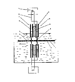
In Figure 1, there are situated on both sides of the circuit board 1 structures 2 which
are to be treated electrochemically, here electroplated. The structures are
electrically conductive. They can be created, for example, by etching and have no
electrical connection amongst themselves. Hence, contacting of the structures at
one single point on the circuit board, as is common with known methods for
producing circuit boards, is not possible. The metallic fibres 3 of the brushes 4 serve
in the present device for contacting the structures 2. The fibres 3 rest lightly on the
surfaces of the structures 2 to be treated. Together with the connection lines 6, they
thus produce the electrical connection of the surfaces to the bath current source 7
via the brushes 4. The other pole of the bath current source 7 is connected to the
counter-electrode 8. This electrode is situated, electrically insulated, between the
brushes 4.~ The active electrode surface 9 is situated near the electrically contacted
structures 2. In Figure 1, the bath current source is shown polarised in such a way
that the device is accommodated for example to the electrochemical deplating of the
circuit boards. From time to time, the counter-electrode 8 needs to be deplated.
This can take place by means of cyclical electrode exchange, the electrodes of the
device being removed and deplated in a separate device. During electrochemical
reduction without dissolved metal in the treatment solution, the exchange of brushes
is inapplicable since nothing is deposited on them.
In Figure 2, the brushes 10, 11, 12, 13 are arranged movably. Two brushes
respectively are held by one rocker 14. The preferably current-regulated bath
current source 7 is polarised here for the brushes 10 and 12 in such a way as is
necessary for electroplating. The brushes 10 and 12 thus have cathodic potential via
the reversing switch 15. The structures 2 on the circuit board are electrically
contacted via said brushes. The brushes 11 and 13, which are raised by the rocker
14, are polarised anodically via the reversing switch 15. They operate as anodes.
At the same time they are deplated if they were previously electroplated. In order to
focus the electroplating and deplating process on the circuit board and on the fibres
of the brushes, there is situated between two brushes respectively a dividing wall 16,
which has an electrically insulating effect so that a direct flow of current between the
differently polarised brush electrodes is generally prevented.
_ _ , . . . . . . .... .. . . .
CA 022~0020 1998-09-24
_ .
After completion of the deplating of the brushes 11 and 13, the latter are brought to
the circuit board surface by means of rockers 14 while, at the same time, brushes 10
and 12 are raised from the surface. The polarity of the brushes changes thereby in
accordance with the drawing. In practice, the brushes can be arranged preferably at
a smaller spacing than is shown in Figure 2. The raising and lowering of the brushes
can also be carried out by other mechanical means. It is not restricted to rockers.
The switching of polarities of the brushes can also be achieved with electronic
switches. The transportation rollers or wheels 17 which are known from through-put
units are shown only in Figure 2. Transportation elements of this type can also be
used in the devices in Figures 1 and 3 to convey the circuit boards through the
device along the direction of transportation which characterised by the arrow shown.
In addition; rollers can also be used to prevent the escape of treatment liquid
situated above the plane of transportation at the inlet to and the outlet from the
device.
In Figure 3, a further embodiment of the invention is shown. Anodes 20 and brushes
21 are arranged alternately in the through-put direction of the item to be treated.
They extend transversely to the direction of transportation, which is indicated by the
arrow 22, over the entire unit so that all the structures present on the circuit boards
are conveyed past the brushes and counter-electrodes. The brush electrodes 21 are
movable. They can be raised individually, by a drive not shown, from the circuitboard 23 to be treated or from a metallic deplating plate 24. The brushes 21 areraised above the plate 24 as it passes through. Fibres of the brushes resting on the
circuit board 23 produce the electric connection from the structures to be treated via
connection lines 25 to the reversing switch 26. Via the latter, the negative pole of the
bath current source 27 is connected momentarily to the electroplating brushes. The
electroplating current is set automatically in accordance with the selected current
density relative to the number of cathodically connected brushes respectively. For
this purpose, the item to be treated, the circuit board 23 or the circuit boards are
tracked by the control system of the through-put unit. Switching the brushes on and
off occurs individually in temporally correct sequence. The brushes can be
connected in a similar manner just as is described in the Patent document DE 39 39
681 C2 for connecting anodes in through-put units. With respect to the type and the
. . . ~ .
CA 022~0020 1998-09-24
12
conduct of this control system, reference is made to this publication.
The anodes 20 are preferably insoluble. The metal dissolved in the electrolyte is
deposited not only on the structures of the circuit board 23 but also on the fibres or
fibre points of the brushes. They must be deplated from time to time. In Figure 3,
the transition from electroplating to deplating is represented. For deplating, the
brushes 21 are raised and placed simultaneously via reverse switch 26 on an anodic
potential. The second current source 28, which can be set individually, serves for
deplating. The negative pole of the current source 28 is connected electrically to the
deplating plate 24. In order to contact the deplating plates 24 which are to be
transported like the circuit boards through the unit, sliding contacts 29 or clamps are
used as are known from horizontal electroplating through-put units.
The metal, which is located on the fibres of the brushes, is deposited down onto the
deplating plates 24. In practice, the brushes operate till the metal is completely
detached as soluble anodes which require a smaller bath voltage than the insoluble
anodes by about 0.8 volts to dissolve the metal. The result is that the insoluble
anodes 20 do not start up on account of the potential being too low for them and do
not conduct any electroplating current. After complete removal of the metal from the
fibres, the latter likewise represent insoluble anodes. The anode current then drops
to a value of approximately zero. This circumstance can be used for introducing the
reversal of the brushes. If soluble anodes 20 are used it is practical to separate the
latter electrically from the positive potential of the bar 30 by means of a switch not
shown if deplating is in progress in this region.
The deplating plate 24 and the sliding contacts 29 or clamps can be deplated
chemically or electrochemically in the run-back to the unit loader. The plates can be
delivered also to a metal recycling plant elsewhere.
In a particular development of the invention, the raising of the brushes 21 during
deplating can be omitted. In order to avoid a short circuit in the bath current source
28, the deplating plate 24 is covered on all sides by a thin electrically non-conductive
diaphragm. Apart from here, only the side regions are for contacting the plate.
.-- . ~ . .. .. .... . . . . . .. .. . ..
CA 022~0020 1998-09-24
._.
These regions are not touched by the brushes. The diaphragm may be a chemically
resistant cloth. A textile made of polypropylene for example is very suitable for this
purpose. The anodically connected brushes are deplated via the diaphragm. The
deplating process is highly effective on account of the particularly small
anode/cathode spacing. This permits the length of the momentary deplating section
to be kept short in comparison to the electroplating section. The deplating plates
which are covered by the diaphragm are likewise deplated right through the
diaphragm in a separate part of the transportation track. This deplating can
preferably be performed also electrochemically.
In order to treat the circuit boards on both sides, the device in Figure 3 can also be
built latera11y reversed.
.. . . .. _ _