Note: Descriptions are shown in the official language in which they were submitted.
CA 02250244 1998-09-28
SPECIFICATION
ELECTRIC POWER TRANSMISSION DEVICE AND ELECTRIC POWER TRANSMISSION
ME THOD
Technical Field
The present invention relates to an electric power
transmission device and an electric power transmission method, and
for example, is suitably applied to an electric power transmission
device and an electric power transmission method to be used as a
charger which charges electric power to a secondary battery built
in a portable compact electronic equipment via a noncontact
terminal.
Background Art
In recent years, there has been a sharp rise in demand for
portable compact electronic equipment, such as a small-sized
headphone stereo, combination camera/video tape recorder and
mobile communication terminal. These portable compact electronic
equipment are equipped with rechargeable and high capacity
secondary batteries as their power source and are charged by using
a prescribed charger.
One type of the charger devices is a contact type. This
contact type charger has such as a spring-loaded point of contact,
and by contacting a point of contact of the portable compact
1
CA 02250244 1998-09-28
electronic equipment side to the point of contact to electrically
connect them, and the charging current is supplied to the
secondary battery built in the portable compact electronic
equipment via thus formed electric path.
However, in these chargers, the point of contact may be
oxidized or contaminants may be build up on the point of contact
with time. These oxidation and contaminants cause the
disconnection on the part of these contact points and hinder the
supply of charging current to the secondary battery.
To avoid such problems, a charger using the noncontact type
charging system has been considered. As the noncontact type
charging system, a system of supplying the charging current from
the charger to the secondary battery by the electromagnetic
induction can be considered.
More specifically, a primary coil is provided on a terminal
of the charger side and a secondary coil is provided on a terminal
of the portable compact electronic equipment, and the primary coil
and the secondary coil are brought close. When an electric current
is fed to the primary coil under this condition, the primary coil
generates the magnetic flux. At this point, if the current to be
fed to the primary coil is turned ON or OFF at established
intervals, the magnetic flux to be generated by the current
induction varies with time. In the secondary coil side, an
inducted electromotive force is generated by the electromagnetic
induction due to the linkage of the magnetic flux which varies
2
CA 02250244 1998-09-28
with time. The primary coil generates alternating current of which
the direction of current is reversed according to the ON/OFF of
the primary coil side as inducted current with the inducted
electromotive force as a power supply. Thus, the noncontact type
charger conducts charging by supplying the inducted current to be
generated in the secondary coil to the secondary battery as the
charging current.
With this arrangement, by bringing the primary coil of the
charger side and the secondary coil of the portable compact
electronic equipment side close, the electric power will be
transmitted from the primary coil side to the secondary coil side
using the magnetic contact by the electromagnetic induction, and
thereby the noncontact type charger can be obtained.
In the charger constructed as described above, the primary
coil and the secondary coil are built in the charger side and the
electronic equipment side respectively, and by transmitting the
power by the electromagnetic induction from the primary coil to
the secondary coil, the noncontact power transmission can be
conducted.
However, in this case, as the distance between the primary
coil and the secondary coil is lengthened (in the case of magnetic
permeability of the air), a coupling coefficient between the
primary coil and the secondary coil becomes worse and the amount
of linkage of the magnetic flux generated in the primary coil to
the secondary coil decreases. Therefor, in the electric power
3
CA 02250244 1998-09-28
transmission device, it is difficult to increase the degree of
coupling between the primary coil and the secondary coil such as
the general transformer.
Accordingly, the electric power transmission device described
above has a problem that the efficiency in the power transmission
becomes low due to the power loss by weak coupling.
Disclosure of the Invention
The present invention has been done considering the above
point and is proposing an electric power transmission device and
an electric power transmission method which are capable of
improving the efficiency in electric power transmission from the
primary coil side to the secondary coil side.
To solve such problems, in the present invention, the
electric power transmission device for transmitting the electric
power between the primary coil and the secondary coil, comprises
signal generating means for generating and transmitting an
oscillation signal formed of a fixed frequency, current supplying
means for supplying the electric current to be conducted to the
primary coil, driving means for drive-controlling the conduction
and interception of the electric current to the primary coil based
on the frequency of the oscillation signal, a primary coil for
generating a magnetic flux which varies with time, based on the
frequency of oscillation signal by drive controlling the
conduction and interception of the electric current, and a
4
CA 02250244 1998-09-28
secondary coil to which a capacitance element is connected in
parallel, for generating an induced electromotive force according
to the linkage of the magnetic flux which varies with time and is
generated in the primary coil, and for performing resonant of the
induced electric current to be generated between the capacitance
element and the secondary coil based on the induced
electromagnetic force with the frequency higher than the frequency
of oscillation signal as the oscillation frequency, so that the
inducted electromotive force can be transmitted to the secondary
coil by the linkage of the magnetic flux which varies with time
and is generated in the primary coil.
Since the frequency higher than the frequency of oscillation
signal of the primary coil side is chosen as the resonant
frequency of the secondary coil side, the capacitance can be
reduced and the coupling coefficient between the primary coil and
the secondary coil can be apparently increased. Thus, the
efficiency in the power transmission from the primary coil side to
the secondary coil side can be improved.
Brief Description of the Drawings
Fig. 1 is a circuit diagram showing the construction of a
charger and an electronic equipment according to the first
embodiment of the present invention.
Fig. 2 is a circuit diagram showing an equivalent circuit of
an electromagnetic induction section.
CA 02250244 1998-09-28
Fig. 3 is a diagram explaining the relation between the
driving frequency of the primary coil and the resonant frequency
of the secondary coil.
Fig. 4 is a diagram explaining the driving voltage to be
given to the primary coil according to the driving frequency.
Fig. 5 is a diagram explaining the induction voltage to be
generated in the secondary coil.
Fig. 6 is a circuit diagram showing the construction of a
charger and an electronic equipment according to the second
embodiment of the present invention.
Fig. 7 is a diagram explaining the induction voltage to be
generated in the secondary coil.
Fig. 8 is a schematic diagram showing the construction of a
charger and an electronic equipment according to the third
embodiment of the present invention.
Fig. 9 is a block diagram showing the construction of a
charger and an electronic equipment according to the fourth
embodiment of the present invention.
Fig. 10 is a diagram explaining the induction voltage control
of the secondary coil side according to the frequency variation of
the primary coil side.
Fig. 11 is a diagram explaining the maintenance of the
induction voltage according to the embodiment.
Fig. 12 is a flow chart explaining the procedure of the
frequency control according to the voltage detection.
6
CA 02250244 1998-09-28
Fig. 13 is a block diagram showing the construction of a
charger and an electronic equipment according to the fifth
embodiment of the present invention.
Fig. 14 is a block diagram showing the construction of a
charger according to the sixth embodiment of the present invention.
Fig. 15 is a block diagram showing the construction of a
charger according to the other embodiment.
Fig. 16 is a block diagram showing the construction of a
charger according to the other embodiment.
Best Mode for Carrying Out the Invention
An embodiment of the present invention will be described in
detail with reference to the accompanying drawings.
(1) The First Embodiment
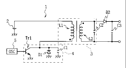
In Fig. 1, numeral 1 generally shows a charger, in which a
secondary battery is recharged by supplying the electric power
sent out from a power source 2 to the secondary battery which is
built in the prescribed electronic equipment via an
electromagnetic induction section 3. The electromagnetic induction
section 3 is comprised of a primary coil L1 placed in the charger
1 side and a secondary coil L2 provided in the electronic
equipment, and these primary coil L1 and the secondary coil LZ do
not have a point of contact with each other. One terminal of the
primary coil L1 is connected to the power source 2, and both
terminals of the secondary coil L2 are connected to the secondary
7
CA 02250244 1998-09-28
battery. The charger 1 is comprised of the primary coil L1 and the
secondary coil L2 which are winded around cores having the fixed
shapes respectively and these cores are placed facing each other
when charging.
In the charger 1, the other terminal of the primary coil L1
is connected to a driving circuit 4 and the driving circuit 4 is
connected to a driving frequency generating unit 5. The driving
frequency generating unit 5 generates an oscillation signal formed
of the prescribed frequency fosc and supplies this to the driving
circuit 4. The driving circuit 4 feeds the supplied oscillation
signal to a base electrode of a transistor Trl which is emitter
grounded. When the voltage level of the oscillation signal entered
into the base electrode is positive value, the transistor Trl
conducts the current between the emitter electrode and the
collector electrode. Thus, the current to be sent out from the
power source 2 flows into the primary coil L1.
Furthermore, in the case where the voltage level of the
oscillation signal to be entered into the base electrode of the
transistor Trl becomes the negative value, the transistor Trl cuts
off the conduction between the emitter electrode and the collector
electrode. Under this condition, the current to be transmitted
from the power source 2 does not flow into the primary coil Ll,
and an LC circuit formed by the primary coil L1 and a capacitor C1
of the driving circuit 4 forms a resonance circuit and an inverse
electromotive force is generated in the primary coil L1. The
B
CA 02250244 1998-09-28
current flows into the capacitor C1 to conduct the charging with
the voltage by this inverse electromotive force as an electric
source, and the current of the opposite direction flows into the
primary coil L1 when the capacitor C1' conducts discharging to the
primary coil L1. The current increases as the voltage of the
capacitor C1 drops, and when the voltage of the capacitor C1
becomes 0, the current becomes the maximum. Then, the capacitor C1
is charged by the voltage of the opposite direction. At the point
of time when the voltage exceeds the voltage of the power source 2,
a damper diode D1 in the driving circuit 4 is conducted and the LC
circuit becomes short-circuited condition and oscillation by the
LC circuit stops and the current flowing into the primary coil L1
decreases linearly. At the time when the current becomes 0, the
transistor Trl becomes ON state, and these operations are repeated
thereafter. In this way, the current flowing into the primary coil
L1 vibrates moving forward and backward alternately by the driving
circuit 4, and accordingly, the voltage to be produced in the
primary coil L1 becomes the form of horizontal pulse that changes
based on the driving frequency fosc to be transmitted from the
driving frequency generating unit 5.
The magnetic flux is generated in the primary coil L1 as the
current flows and the magnetic flux varies over time corresponding
to the oscillation of the current described above. Moreover, the
induced electromotive force is generated in the secondary coil L2
by the linkage of the magnetic flux which varies with time, to the
9
CA 02250244 1998-09-28
secondary coil L2. Thus, the current flows through the secondary
coil L2 by the induced electromotive force which reverses
according to the time-varying magnetic flux, and the resonant
occurs in the current by the secondary coil L2 and a capacitor C2
connected to the secondary coil L2 in parallel. Thus, the
alternating induced current generated in the secondary coil L2 is
sent out via the diode D2. The electronic equipment having the
secondary coil L2 rectifies the induced current to be generated
having the induced electromotive force as the power source, with
the diode D2 and supplies this to the secondary battery to charge.
The charger 1 transmits the electric power to be sent out from the
power source 2 by the electromagnetic induction, from the primary
coil L1 to the secondary coil L2 to charge.
In this connection, Fig. 2 shows an equivalent circuit of the
electromagnetic induction section 3 and LS2 shown in this Fig. is
leakage inductance of the secondary coil L2 side.
At this point, as shown in Fig. 3, in the charger 1, assuming
that the frequency of induction voltage to be generated in the
secondary coil L2 by the induced electromotive force to be
reversed, that is the resonant frequency, is fog, the resonant
frequency fog is set to become higher than the frequency to drive-
control the current flowing through the primary coil 1, that is
the driving frequency fas~. The resonant frequency fog with respect
to the driving frequency fos~ can be set by adjusting the number of
winds of the secondary coil L2 with respect to the number of winds
CA 02250244 2005-04-04
of the primary coil or by adjusting the capacity of the resonant
capacitor C2 connected to the secondary coil L2 in parallel.
As shown in Fig. 4, the current flows through the primary
coil L1 in the forward direction or in the backward direction in
accordance with the ON/OFF condition of the transistor Trl of the
driving circuit 4, and the voltage generated in the primary coil
L1 appears in the form of pulse wave formed of the driving
frequency fos~~ Here, el is a power element to be formed in the
primary coil L1 when the transistor Trl is in the OFF condition,
and eZ is a power element to be generated in the primary coil L1
when the transistor Trl is in the ON condition.
Furthermore, as shown in Fig. 5, induction voltage formed of
the resonant frequency fog is generated according to the temporal
changes of magnetic flux generated in the primary coil L1. Here,
e3 and e, show power elements based on the voltage and current,
which is produced in the secondary coil L2. The power element e3
corresponds to the pov~ter element el and is produced in the
secondary coil L2 when Trl is in the OFF condition. Moreover, the
power element e, corresponds to the power element e2 and is
produced in the secondary coil L2 when Trl is in the ON condition.
At this point, in the electronic equipment comprising the
secondary coil L2, the power is taken by rectifying the induced
current produced at the power element e3 part, and supplied to the
secondary battery. In this connection, since the winding direction
of the primary coil L1 and the winding direction of the secondary
11
CA 02250244 1998-09-28
coil L2 are opposite, the plus and minus of wave forms of the
driving frequency to be formed in the primary coil L1 and the
resonant frequency to be formed in the secondary coil L2 are
reversed.
According to the foregoing construction, the transistor Trl
of the driving circuit 4 becomes ON/OFF condition according to the
frequency of the oscillation signal to be formed in the driving
frequency generating unit 5, and when it is in the ON condition,
the current to be supplied from the power source 2 flows through
the primary coil L1. Moreover, when the transistor Trl is in the
OFF condition, an inverse electromotive force is generated in the
primary coil Ll and the capacitor C1 is charged. Thereafter, the
capacitor C1 is discharged, thereby the current flows in the
direction opposite to the time when the transistor Trl is in the
ON condition. Thus, the magnetic flux produced in the primary coil
L1 varies with time in accordance with the inversion of the
current direction.
An induced electromotive force is generated in the secondary
coil L2 by the linkage of magnetic flux produced in the primary
coil L1 and the direction of the induced electromotive force
changes according to the temporal changes of magnetic flux. Thus,
in the secondary coil L2, an induction voltage is generated by the
resonant frequency fog with respect to the driving frequency fos~ bY
the inversion of the induced electromotive force.
At this point, in the case where the resonant frequency fog
12
CA 02250244 1998-09-28
by the LC circuit of the secondary coil L2 side is set to become
the same frequency as the driving frequency fos~ of the primary coil
L1, the current level becomes maximum when the voltage level is
the largest since the current to be conducted into the primary
coil L1 is in phase with the voltage due to the resonance. When
the secondary coil L2 side is resonated with such frequency, the
power loss by the internal impedance on the LC circuit of the
secondary coil L2 side becomes large and the efficiency in the
power transmission cannot be improved.
Furthermore, in the case where the resonant frequency fog is
set to become lower than the driving frequency fas~ of the primary
coil L1, the current value of the induced current to be produced
in the secondary coil L2 side becomes small because it is
resonated with the frequency departed from the frequency of the
driving frequency fosc~ However, since the time required for
discharging the resonant capacitor C2 connected to the secondary
coil L2 in parallel becomes longer, the capacitance C equivalently
becomes large and the actual efficiency Q decreases, so that the
high output voltage cannot be obtained.
The induced current to be generated in the secondary coil L2
is formed of the alternating current as described above, and by
decreasing the induced current while increasing the induction
voltage, the power can be taken efficiently decreasing the power
loss due to the internal impedance. Therefor, the induction
voltage to be obtained in the secondary coil L2 side is required
13
CA 02250244 1998-09-28
as high as possible.
Accordingly, as described above, in the charger 1, since the
resonant frequency fog of the secondary coil L2 side is set to
become higher than the driving frequency fosc of the primary coil L1
side, the resonant current can be made into low current and the
capacitance C in the resonant circuit of the secondary coil L2 can
be equivalently made smaller and the actual efficiency Q can be
increased. Thus, in the charger 1, by increasing the apparent
coupling coefficient, the efficiency in the power transmission
from the primary coil L1 to the secondary coil L2 can be improved.
Furthermore, in the electronic equipment having the secondary
coil L2, the part of power element e3 at the time when the
transistor Trl is in the OFF condition is rectified, thereby the
power is taken from the induced current to be generated in the
secondary coil L2 responding to the direction inversion of the
current flowing through the primary coil L1. More specifically,
regarding the power elements e3 and e4 (Fig. 5), areas of these
elements are the same, and thus, the following relationship exists
in these power elements; the width of the current T2 of the power
element e4 is narrower than the width of the current T1 of the
power element e3, while the voltage value of the power element e4
is larger than the voltage value of the power element e3.
Accordingly, in the case where the electric power element e, part
is rectified and taken as the power, high output voltage can be
obtained. However, since the width of current T2 is narrower than
14
CA 02250244 1998-09-28
the width of current T1 of the power element e3, the conduction
angle of rectification is narrow and becomes an unstable output
source as compared with the case where the power element e3 is
rectified.
In the charger 1, since the electronic equipment having the
secondary coil L2 rectifies the induced current of the power
element e3 part and takes out the power, the conduction angle of
rectification can be made wider and a stable source power can be
obtained.
According to the foregoing construction, in the case of
transmitting the electric power from the primary coil L1 to the
secondary coil L2 by the electromagnetic induction between the
primary coil L1 and the secondary coil L2, since the resonant
frequency fag to be produced in the secondary coil L2 side is set
to become higher than the driving frequency fos~ of the primary coil
L1 and the resonant voltage of the power element e3 part at the
time when the transistor Trl is in the OFF condition is rectified
to take out the source power from the resonant voltage produced in
the secondary coil L2, the actual efficiency Q can be increased
and the apparent coupling coefficient can be increased and at the
same time, the power of the power source can be obtained from the
resonant voltage having the wide conduction angle of rectification.
Thus, the efficiency in power transmission can be increased and
the stable current power can be obtained.
(2) The Second Embodiment
CA 02250244 1998-09-28
In Fig. 6 in which the same reference numerals are applied to
parts corresponding to Fig. 1, numeral 10 shows a charger having a
source 2, an electromagnetic induction section 3, a driving
circuit 4 and a driving frequency generating unit 5, similar to
that of the battery device 1. The charger 10 has the primary coil
L1 which is winded around a core having the fixed shape as the
electromagnetic induction section 3 (Fig. 1), and when charging,
the secondary coil L2 winded around a core arranged in the
electronic equipment is placed at a position facing the core
winded by the primary coil L1.
The charger 10 drive-controls the conduction and interception
to the primary coil L1 by turning the transistor Trl of the
driving circuit 4 into the ON/OFF condition by the oscillation
signal to be formed in the driving frequency generating unit 5 in
order to flow the current through the primary coil L1 in the
forward direction and the backward direction alternately. Thus,
the time-varying magnetic flux is generated in the primary coil L1
by the current flowing in the forward direction and the backward
direction, and an induced electromotive force is produced in the
secondary coil L2 by the linkage of the magnetic flux, so that the
resonant current flows by the LC resonance circuit formed of the
secondary battery L2 and the capacitor C2 connected to the
secondary coil L2 in parallel. The charger 10 is arranged in order
that the resonant frequency of the secondary coil L2 becomes
higher than the driving frequency of the primary coil L1 as in the
16
CA 02250244 1998-09-28
case of the charger 1 (Fig. 3).
In addition, in the charger 10, the secondary coil L2 is
formed by connecting two coils which are winded around in the same
direction, while in the charger 1 in which the secondary coil L2
is formed with a single coil. More specifically, the charger 10
forms an electromagnetic induction section 3 by connecting coils
L2A and L2B in series as the secondary coil L2, and after
rectifying the voltage of the resonance circuit to be obtained by
the inducted electromotive force generated according to the
linkage of the magnetic flux, which is formed in the primary coil
L1, toward the secondary coil L2, with diodes D2 and D3
respectively, supplies this into the secondary battery as a power
source output.
Since the secondary coils L2A and L2B are winded around the
cores in the same direction, as shown in Fig. 7, in the polarity
of resonant frequency of the secondary coil L2 with respect to the
driving frequency of the primary coil L1, their phases shift each
other by 180(' ) observing from a standard point A on which the
secondary coils L2A and L2B are connected. In the electronic
equipment having the secondary coils L2A and L2B, the resonant
voltage generated based on the resonant frequency is rectified and
taken out by the diodes D2 and D3 as the power, and the taken
power is supplied to the secondary battery to charge.
At this point, in the case where the winding numbers of wires
winded around cores of the secondary coil L2A and L2B are the same,
17
CA 02250244 1998-09-28
the voltage of the power element e~" to be formed in the secondary
coil L2A when the transistor Trl is in the OFF condition is
smaller than the voltage of the power element e2H to be formed in
the secondary coil L2B when the transistor Trl is in the ON
condition. In the case where the power is taken out after
rectifying the resonant voltage of the power elements e2" and eze.
the difference between these voltages becomes the variable value
and unstable electric power. Accordingly, by adjusting the winding
numbers of the secondary coil L2A and L2B, about equal values of
voltage can be obtained in the secondary coil L2 side. More
specifically, the winding number of the secondary coil L2A is
arranged to become larger than the winding number of the secondary
coil L2B, and thus, the voltage values of resonant voltages to be
obtained in the secondary coil L2A and L2B become approximately
th a s ame .
According to the foregoing construction, as to the resonant
frequency to be generated in the secondary coil L2 side in
accordance with the driving frequency of the primary coil L1 side,
the resonant frequency of the secondary coil L2A and the resonant
frequency of the secondary coil L2B have phases shift each other
by 180 0 ), and the induced currents produced based on such
resonant frequencies are rectified respectively by the diodes D2
and D3 and sent out. At this point, the ratio of the winding
number of coil between the secondary coil L2A and L2B is adjusted
so that the winding number of coil of the secondary coil L2A is
18
CA 02250244 1998-09-28
larger than the winding number of coil of the secondary coil L2B
and the induction voltage to be generated in the secondary coil
L2A and the induction voltage to be generated in the secondary
coil L2B become approximately the same values.
Accordingly, upon rectifying the induced current of the
secondary coil L2A and the induced current of the secondary coil
L2B of which resonant frequencies have phases shifting each other
by 180 0 ) and outputting them, the induced current of the power
element eZA formed in the secondary coil L2A and the induced
current of the power element e2H formed in the secondary coil L2B
according to the time-varying of magnetic flux of the primary coil
L1 can be taken out as the electric power, and the electric power
can be taken out in either case where the transistor Trl is in the
ON or OFF condition.
Furthermore, by adjusting the ratio of winding number of the
secondary coils L2A and L2B, voltage values of the power elements
e2" and ezB are to become approximately the same, and accordingly,
the stable electric power of which the voltage variation is
controlled can be obtained.
According to the foregoing construction, since the resonant
frequency to be formed in the secondary coil L2 side is arranged
so as to become higher than the driving frequency of the primary
coil L1, and the secondary coils L2A and L2B having about equal
values of induction voltages which can be obtained by adjusting
the winding number of the secondary coil L2A becomes larger than
19
CA 02250244 1998-09-28
the winding number of the secondary coil L2B are connected and
placed in the electronic equipment and the resonant voltages to be
formed respectively are rectified and sent out. Thereby, the
apparent coupling coefficient can be increased by increasing the
efficiency factor Q and at the same time, the resonant voltages of
the power elements e2A and ezB to be produced in the secondary coils
L2A and L2B can be taken out as the source power. Thus, the
efficiency in power transmission from the primary coil L1 to the
secondary coil L2 can be improved and the stable power can be
obtained regardless of the current direction of the primary coil
L1.
(3) The Third Embodiment
In Fig. 8, in which the same reference numerals are applied
to parts corresponding to Fig. 1, numeral 20 shows a charger
comprised of a power source 2, an electromagnetic induction
section 3, a driving circuit 4 and a driving frequency generating
unit 5 which have the same construction as the charger 1. The
charging unit 20 has the primary coil L1 winded around a core of
the fixed shape as the electromagnetic induction section 3 (Fig.
1), and when charging, the core winded by the secondary coil L2
provided in the electronic equipment is placed on the position
facing the core winded by the primary coil Ll.
The charger 20 drive-controls the conduction and interception
to the primary coil L1 by turning the transistor Trl of the
driving circuit 4 ON or OFF by the oscillation signal generated in
CA 02250244 1998-09-28
the driving frequency generating unit 5 in order to supply the
current to the primary coil Ll in the forward direction and the
backward direction alternately. Thus, the time-varying magnetic
flux is generated in the primary coil L1 by the current flowing in
the forward direction and the backward direction, and an induced
electromotive force is formed in the secondary coil L2 by the
linkage of the magnetic flux, and resonant current flows by the LC
circuit of the secondary coil L2 and the capacitor C2 connected in
parallel to the secondary coil L2. In this connection, the charger
20 is so arranged that the resonant frequency of the secondary
coil L2 becomes higher than the driving frequency of the primary
coil L1 as in the case of charger 1.
As compared with the construction of the charger 1, the
charger 20 is different from the charger 1 on the loading
condition of the primary coil L1 and the secondary coil L2 and
sizes of cores winded by the coils. The cross sectional area of
the core winded by the secondary coil L2 is smaller than the cross
sectional area of the core winded by the primary coil L1, and when
charging, the core winded by the primary coil L1 and the core
winded by the secondary coil L2 are placed, in which their centers
shift each other.
More specifically, in the charger 20, the core of the primary
coil L1 side has the fixed ring shape and a part of the core is
cut off at the fixed position on the ring and separated by the
fixed distance. Moreover, when charging, the core winded by the
21
CA 02250244 2005-04-04
secondary coil L2 is inserted between the opposite cross sections
spaced and is placed facing each cross section. Furthermore, when
charging, the charger 20 places the secondary coil L2 in order
that the center of the core winded by the secondary coil L2 is
shifted from the center of the core winded by the primary coil L1
in the desired direction.
For example, as shown in Fig. 8, in the charger 20, by locating
the position of the outer region of the core winded by the
secondary coil L2 onto the position of one of the outer regions of
the core winded by the primary coil L1, the core of the secondary
coil L2 side is placed on the position shifted from the center of
the core of the primary coil side. In the charger,20, the resonant
frequency of the secondary coil L2 is set to become higher than
the driving frequency of the primary coil L1 according to such
arrangements.
According to the foregoing construction, the core winded by
the secondary coil L2 is inserted between the cross sections
separated of the core winded by the primary coil L1 and its center
of the core is placed on the position shifted from the center of
the core of. the primary coil L1 side. Moreover, in the secondary
coil 2 side, the resonant frequency is set to~become higher than
the driving frequency of the primary coil L1 side on the position.
The magnetic flux is generated between the cross sections of
each core of the primary coil L1 side, which are separated by the
fixed distance, by the current flowing through the primary coil L1,
22
CA 02250244 1998-09-28
and the driving circuit 4 reverses the direction of current
flowing through the primary coil L1 based on the frequency of the
oscillation signal to be transmitted from the driving frequency
generating unit 5 in order to change the magnetic flux to be
produced in the primary coil L1 over time. Thus, the induced
electromotive force which reverses in accordance with the time-
varying magnetic flux is generated in the secondary coil L2, and
the induced current can be obtained with the induced electromotive
force as an electric source.
However, in this case, magnetic energy of the magnetic flux
causes linkage between the other parts stored in the electronic
equipment having the secondary coil L2 and affects these parts and
there are cases where heat is generated or operation errors occur.
In the battery device 20, since the core winded by the
secondary coil L2 is placed on the position at least separate from
the center of the core of the primary coil L1, the effect of
magnetic flux to the other electronic parts in the electronic
equipment equipped with the secondary coil L2 is and thereby the
generation of heat caused by the magnetic field and operation
errors can be prevented.
Furthermore, since the cross sectional area of the core of
the secondary coil L2 side is made smaller than the cross
sectional area of the core of the primary coil L1 side, if the
cores are placed on positions shifted each other, scattering of
the magnetic field to be formed between the primary coil L1 and
23
CA 02250244 1998-09-28
the secondary coil L2 can be decreased. Furthermore, since the
cross sectional area of the core is made smaller, a storage
capacity of the secondary coil core in the electronic equipment
having the secondary coil L2 can be made smaller, thus, the
electronic equipment can be minimized.
Also in this case, since the resonant frequency is set to
become higher than the driving frequency under such arrangements,
the efficiency in power transmission from the primary coil L1 side
to the secondary coil L2 side can be improved.
According to the foregoing construction, since charging is
conducted under the condition in which the resonant frequency of
the secondary coil L2 side is higher than the driving frequency of
the primary coil L1 side, and as well as making the cross
sectional area of the secondary coil L2 side smaller than the
cross sectional area of the core of the primary coil L1 side, the
core winded by the secondary coil L1 is placed on the position
shifted from the center of the core winded by the primary coil L1,
the efficiency factor Q can be made higher and apparent coupling
coefficient can be made higher, the effect of the magnetic flux
produced in the primary coil L1 with respect to the electronic
equipment in the electronic equipment can be decreased. Thereby,
as well as the efficiency in electric power transmission from the
primary coil L1 to the secondary coil L2 can be improved, the
generation of heat or the operation error due to influence of the
magnetic field can be prevented and furthermore, miniaturization
24
CA 02250244 1998-09-28
of the electric equipment can be realized.
(4) The Fourth Embodiment
In Fig. 9 in which the same reference numerals are applied to
parts corresponding to Fig. 1, numeral 30 shows a charger
comprised of a source 2, an electromagnetic induction section 3
and a driving circuit 4 as the similar construction to the charger
1. The charger 30 is comprised of the primary coil L1 which winds
around the core having the fixed shape as an electromagnetic
induction section 3, and when charging, the core winded by the
secondary coil L2 placed in the electronic equipment is placed at
the position facing the core winded by the primary coil L1.
The charger 30 turns the transistor Trl of the driving
circuit 4 ON/OFF by an oscillation signal generated in the driving
frequency generating unit 5 to drive-control the conduction and
interception to the primary coil L1 and flows the current to the
primary coil L1 in the forward direction and the backward
direction alternately. Thus, by the current flowing in the forward
direction and the backward direction, a time-varying magnetic flux
is generated in the primary coil L1 and an induced electromotive
force is produced by the linkage of the magnetic flux and resonant
current flows and resonance occurs by the LC circuit. The charger
30 is arranged so that the resonant frequency of the secondary
coil L2 becomes higher than the driving frequency of the primary
coil L1 as in the case with the charger 1 (Fig. 3).
The charger 30 is constructed differently from the charger 1
CA 02250244 1998-09-28
with the added devices, comprising a variable frequency generating
unit 31 capable of varying the frequency of oscillation signal to
be generated in place of the driving frequency generating unit 5
(Fig. 1), a voltage detection unit 32, a oscillation frequency
control unit 33, and an input voltage control unit 34. The charger
30 controls the variable frequency generating unit 31 by the
oscillation frequency control unit 33 depending on the detection
result of the voltage by the voltage detection unit 32 and
simultaneously controls an input voltage to be supplied from the
power source 2 by the input voltage control unit 34. Thus, the
frequency and input voltage of the oscillation signal varies.
The variable frequency generating unit 31 supplies the
generated oscillation signal to the driving circuit 4. The driving
circuit drive-controls the current to be conducted to the primary
coil L1 in accordance with the voltage level of the oscillation
signal to flow the current in the forward direction and the
backward direction alternately. Accordingly, the magnetic flux
generated in the primary coil L1 varies with time. The secondary
coil L2 generates an induced electromotive force in accordance
with the linkage of the magnetic flux to be generated in the
primary coil L1 and obtains an induced current which reverse
according to the time-change of the magnetic flux with the induced
electromotive force as the power source.
At this point, if the secondary battery is connected to the
connection terminal of the electronic equipment having the
26
CA 02250244 1998-09-28
secondary coil LZ as a load, an output voltage V of the secondary
coil L2 side drops due to the load. Such output voltage drop
affects the primary coil L1 side causing drop in the voltage to be
generated in the primary coil L1. The charger 30 detects such
voltage drops caused by the load, by the voltage detection unit 32
connected to the primary coil L1 in parallel. Moreover, since the
case where the power source voltage rises by the power source 2
can be considered, the charger 30 also detects the voltage rise by
the voltage detection unit 32.
The reference voltage is set in advance in the voltage
detection unit 32 and at the time when the drop or rise of the
voltage is detected, a detection signal S1 is sent to the
oscillation frequency control unit 33 and the input voltage
control unit 39.
The oscillation frequency control unit 33 supplies a control
signal S2 to the variable frequency generating unit 31 in
accordance with the detection signal S1, and when the voltage drop
is detected, rises the frequency of oscillation signal formed by
the variable frequency generating unit 31, and when the voltage
rise is detected, drops the frequency of the oscillation signal
formed by the variable frequency generating unit 31. Furthermore,
the input voltage control unit 34 controls the input voltage
supplied from the power source 2, in accordance with the detection
signal S1, and when the voltage drop is detected, the input
voltage control unit 34, after rising the input voltage, sends it
27
CA 02250244 1998-09-28
out to the primary coil L1, and when the voltage rise is detected,
after dropping the input voltage, sends it out to the primary coil
L1.
The value of the induction voltage to be generated in the
secondary coil L2 side is set to become the maximum value at the
time when the resonant frequency fog, i.e., the induced current
produces resonance. The charger 30 adjusts the driving frequency
fosc within the fixed frequency range under the resonance frequency
fo"z, of the secondary coil L2 side by the variable frequency
generating unit 31. Thus, in the charger 30, the driving frequency
varies within the variable range by the variable frequency
generating unit 31, and by changing the resonance frequency in the
primary coil L1 side, the induction voltage to be generated in the
secondary coil L2 side is risen or dropped.
As shown in Fig. 10, for example, by rising the frequency of
oscillation signal, i.e., the driving frequency from fl by Ofl, the
induction voltage V2 to be generated in the secondary coil L2 can
be risen by ~V2.
Accordingly, as shown in Fig. 11, when the induction voltage
drops as shown by a solid line in Fig. because the load is
connected, the charger 30 detects the drop of the induction
voltage indirectly by the voltage detection unit 32, and as a
result of this detection, controlling the variable frequency
generating unit 31 by the oscillation frequency control unit 33,
rises the frequency of the oscillation signal, and simultaneously
28
CA 02250244 1998-09-28
rises the power source voltage to be supplied from the power
source 2 by the input voltage control unit 34 and supplying it to
the primary coil L1. Thereby, the induction voltage can be
increased by the voltage value dropped and the fixed voltage can
be maintained as shown by a broken line in Fig. In this connection,
when the voltage rises, controlling the frequency and the voltage
by the oscillation frequency control unit 33 and the input voltage
control unit 34, the fixed voltage is maintained.
The charger 30 performs maintenance of the induction voltage
to be generated in the secondary coil L2 side according to the
procedure shown in Fig. 12. More specifically, firstly the charger
30 starts the procedure at step SP1. After starting the procedure,
at step SP2, the charger 30 detects the voltage changes occurred
in the primary coil L1 by the voltage detection unit 32. The
charger 30 judges the detection result by using the detection
signal S1. If the voltage drop is recognized at step SP3, it
proceeds to step SP5. In addition, if the voltage drop is not
recognized as the detection result by the detection signal S1, it
proceeds to step SP4. The charger 30 judges the detection result
by using the detection signal S1 and if the voltage rise is
recognized at step SP4, proceeds to step SP6. Moreover, if the
voltage rise is not recognized as the detection result by the
detection signal S1, returns to step SP2.
When the voltage drop is recognized at step SP3, the charger
30 raises the frequency fl of the oscillation signal by ~ fl, at
29
CA 02250244 1998-09-28
step SP5, according to the control of the variable frequency
generating unit 31 by the oscillation frequency control unit 33,
and raises the input voltage Vl by ~V1 according to the control of
the input voltage by the input voltage control unit 34. Moreover,
if the voltage rise is recognized at step SP4, the charger 30, at
step SP6, lowers the frequency fl of the oscillation signal by D fl
according to the control of the variable frequency generating unit
31 by the oscillation frequency control unit 33, and also lowers
the input voltage V1 by OV1 according to the control of the input
voltage by the input voltage control unit 34.
With the above arrangement, after conducting the frequency
control and input voltage control, the charger 30 returns to step
SP2 and repeats the procedure till the voltage drop or rise are
not detected by the voltage detection, and by controlling the
driving frequency and input voltage, compensates for the amount of
voltage drop or rise of the induction voltage in the secondary
coil L2 side.
According to the foregoing construction, the charger 30
detects the voltage changes occurred in the primary coil L1 by the
voltage detection unit 32. When the voltage drop, i.e., the drop
of induction voltage to be generated in the secondary coil L2 side,
is detected by the detection, the charger 30 informs the detection
result to the oscillation frequency control unit 33 and the input
voltage control unit 34 by using the detection signal S1. The
oscillation frequency control unit 33 controls the variable
CA 02250244 1998-09-28
frequency generating unit 31 in accordance with the information
and raises the frequency of the oscillation signal. Moreover, the
input voltage control unit 34, after controlling and increasing
the power source voltage to be supplied from the power source 2,
transmits it to the primary coil L1.
Accordingly, the charger 30 can increase the induction
voltage of the secondary coil L2 side indirectly by controlling
the frequency and the input voltage of the oscillation signal. And
if the induction voltage drops by connecting the load in the
secondary coil L2 side, the charger 30 can increase the induction
voltage by controlling the driving frequency and the input voltage,
and maintain the induction voltage at the constant level to make
it stable. When the voltage rises, the charger 30 can decrease the
induction voltage in the same manner and thus, can maintain the
induction voltage at the constant level to make it stable.
Furthermore, the charger 30 is arranged to increase or
decrease the voltage by the control of the input voltage by the
input voltage control unit 34 as well as the control of the
driving frequency by the oscillation frequency control unit 33.
Thus, the induction voltage can be corrected accurately by using
the frequency control at the same time.
According to the foregoing construction, as well as
increasing the resonant frequency of the secondary coil LZ side as
compared with the driving frequency of the primary coil L1 side,
and providing the variable frequency generating unit 31, the
31
CA 02250244 1998-09-28
voltage detection unit 32, oscillation frequency control unit 33
and the input voltage control unit 34, if the voltage change is
detected by the voltage detection, the driving frequency and the
input voltage are controlled, thereby the driving frequency and
the input voltage can be controlled and the induction voltage can
be corrected indirectly at the time when the induction voltage
varies in the secondary coil L2 side. Thus, the efficiency in the
electric power transmission from the primary coil L1 to the
secondary coil L2 can be improved and the induction voltage can be
kept constant and stabilized.
(5) The Fifth Embodiment
In Fig. 13 in which the same reference numerals are applied
to parts corresponding to Fig. 9, numeral 40 generally shows a
charger and basically has a configuration similar to that of the
charger 30 (Fig. 8). More specifically, the charger 40 flows the
current to be supplied from the power source 2, to the primary
coil L1 based on the frequency of the oscillation signal to be
generated by the variable frequency generating unit 31, and
generates the induced electromotive force in the secondary coil L2
side by the electromagnetic induction according to the changes of
magnetic flux which is formed in the primary coil L1, and
transmits the electric power. Moreover, the charger 40 detects the
voltage changes by the voltage detection unit 32 and corrects the
voltage changed depending on the detection result. Note that, the
resonant frequency in the secondary coil L2 is set to become
32
CA 02250244 1998-09-28
higher than the driving frequency of the primary coil L1 (Fig. 3)
just as the charger 1 (Fig. 1).
The construction of the charger 40 differs from that of the
charger 30 in that a driving circuit 41 for flowing the current
periodically to the primary coil L1 in accordance with the
frequency of the oscillation signal is provided in place of the
driving circuit 4 which flows the current to the primary coil L1
in the forward and backward directions in accordance with the
frequency of the oscillation signal, a damper diode D4 is
connected to the primary coil L1 by another coil, and a pulse
width control unit 42 is provided between the variable frequency
generating unit 31 and the driving circuit 41 as well as
eliminating the voltage control unit 34 (Fig. 9).
In the charger 40, the driving circuit 41 is comprised of
only the transistor Trl and no capacitor is provided. In the
charger 30, the magnetic flux varies with time by oscillating the
current flowing through the primary coil L1 by the LC circuit
comprised of the primary coil L1 and the capacitor C1 provided in
the driving circuit 4 and turning the transistor Trl ON and OFF.
The driving circuit 41 inputs an oscillation signal to be
supplied from the variable frequency generating unit 31 via the
pulse width control unit 42 to the base electrode of the
transistor Trl. When the voltage level of the oscillation signal
entered to the base electrode is positive, the transistor Trl
conducts the current between the emitter electrode and the
33
CA 02250244 1998-09-28
collector electrode. Thus, the current to be transmitted from the
power source 2 flows through the primary coil L1.
Furthermore, in the case where the voltage level of the
oscillation signal to be entered to the base electrode of the
transistor Trl becomes the negative value, the transistor Trl
intercepts the conduction between the emitter electrode and the
collector electrode. Thus, the driving circuit 41 gives the pulse
voltage based on the driving frequency of the oscillation signal
to the primary coil L1 and periodically delivers the current to be
sent out from the power source 2 to the primary coil L1. The
magnetic flux to be generated in the primary coil L1 varies over
time when the current is flowing and not flowing, and the induced
electromotive force generated in the secondary coil L2 reverses
due to the linkage of the magnetic flux. Accordingly, the induced
current using the induced electromotive force as the power source
is resonated by the LC circuit comprised of the secondary coil LZ
and the capacitor C2 connected in parallel to the secondary coil
L2 .
The charger 40 supplies the pulse voltage to the primary coil
L1 on the basis of the driving frequency of the oscillation signal
and thus flowing the periodic current, generates an induced
current in the secondary coil L2 side.
Furthermore, the charger 40 detects the voltage change of the
primary coil L1 by the voltage detection unit 32. When the load is
connected to the connection terminal of the secondary coil L2, the
34
CA 02250244 1998-09-28
induction voltage varies due to the load and the voltage drops.
Such induction voltage drop affects the primary coil L1 and causes
the driving voltage drop. The charger 40, by detecting the voltage
change of the primary coil L1 by the voltage detection unit 32,
indirectly detects the voltage change in the induction voltage of
the secondary coil L2.
The predetermined reference voltage value is set in advance
in the voltage detection unit 32, and when the voltage change is
detected by comparing with the reference voltage value, the
detection result is notified by transmitting the detection signal
S1 to the frequency control unit 33 and the pulse width control
unit 42.
At the time when the voltage change is notified by the
detection signal S1, the frequency control unit 33 transmits a
control signal S2 to the variable frequency generating unit 31.
Then, the variable frequency generating unit 31 changes the
frequency of oscillation signal by the predetermined frequency in
accordance with the control signal S2 and transmits this. More
specifically, when the voltage drop is detected, the frequency
control unit 33 outputs the control signal S2 and increases the
frequency of oscillation signal which is transmitted by the
variable frequency generating unit 31, i.e., the driving frequency
by O fl. On the other hand, when the voltage rises, the frequency
of the oscillation signal drops by O fl. Accordingly, the induction
voltage in the secondary coil L2 side drops by ~VZ (Fig. 9).
CA 02250244 1998-09-28
Furthermore, the pulse width control unit 42, when the
voltage change is informed by the detection signal S1, changes the
pulse width of the oscillation signal to be transmitted from the
variable frequency generating unit 31, according to the pulse
width modulation processing to supply this to the driving circuit
41. Specifically, the pulse width control unit 42 narrows the
pulse interval by the fixed interval by modulating the pulse width
during the period in which the voltage level of the oscillation
signal is negative value. Accordingly, the charger 40, by
narrowing the pulse width of the period in which the voltage level
of the oscillation signal is negative value, shortens the cut-off
period of the current by the driving circuit 41.
The pulse width control unit 42, by narrowing the pulse width
of the period in which the voltage level of the oscillation signal
is negative value, can shorten the period in which the transistor
Trl is in the off condition. Since the period in which the
transistor Trl is in the off condition becomes shorter and the
induction period becomes longer, the input impedance is
equivalently decreased and thus, the pulse voltage to be given to
the primary coil L1 can be increased.
When the charger 40 indirectly detects the voltage change
according to the load of the secondary coil L2 side, it controls
the input voltage of the primary coil L1 by performing the
variable control of the driving frequency by the frequency control
unit 33 and the pulse width modulation control during the period
36
CA 02250244 1998-09-28
in which the voltage level of the oscillation signal is negative
by the pulse width control unit 42, and variable-controls and
corrects the induction voltage generated in the secondary coil L2.
According to the foregoing construction, the charger 40 sets
the resonant frequency to be generated in the secondary coil L2 to
become higher than the driving frequency just as in the case of
the charger 1, and simultaneously indirectly detects the voltage
changes caused by the load of the secondary coil L2 side, by
detecting the voltage change of the primary coil L1.
When the charger 40 detects the voltage drop, it increases
the frequency of the oscillation signal (driving frequency) to be
generated by the variable frequency generating unit 31 and
simultaneously, narrows the pulse width during the period in which
the voltage level of oscillation signal is negative. Moreover,
when the charger 40 detects the voltage rise, it widens the pulse
width during the period in which the voltage level of oscillation
signal is negative as well as lowering the frequency of
oscillation signal to be generated by the variable frequency
generating unit 31, that is, the driving frequency.
At the time when the voltage drop is detected, the induction
voltage to be generated in the secondary coil L2 is changed to
high voltage by increasing the driving frequency according to the
frequency control. Since the variable range of driving frequency
is set at the preceding part of the resonant frequency in which
the induction voltage becomes maximum, the induction voltage can
37
CA 02250244 1998-09-28
be increased by increasing the driving frequency.
Similarly, when the voltage drop is detected, by narrowing
the pulse width during the period in which the voltage level of
the oscillation signal is negative, the current conducting period
by the transistor Trl in the driving circuit 41 is made longer.
Thus, by equivalently decreasing the internal resistance of the
transistor Trl, the input voltage to the primary coil L1 can be
increased. Thus, the induction voltage to be generated in the
secondary coil L2 side can be increased indirectly.
In the case where the voltage drop occurs in the driving
voltage, the charger 40 raises the input voltage of the primary
coil L1 by performing the frequency control and the pulse width
modulation control, and thus indirectly raising and correcting the
induction voltage decreased in the secondary coil L2 side due to
the load connection, the voltage can be maintained at a constant
level.
According to the foregoing construction, when the voltage
change occurs in the secondary coil L2 side, by detecting the
voltage changes of the input voltage to be generated in the
primary coil L1 by the voltage detection unit 32, the voltage
change of the secondary coil L2 can be detected indirectly, and
also by raising or lowering the input voltage and driving
frequency of the primary coil L1 by controlling the frequency and
pulse width of the oscillation signal by the frequency control
unit 33 and the pulse width control unit 42, the induction voltage
38
CA 02250244 1998-09-28
to be generated in the secondary coil L2 side can be increased or
decreased indirectly. Accordingly, by detecting the voltage
changes due to the load connection of the secondary coil L2 side
to correct the changed voltage, the voltage can be maintained at a
constant level.
(6) The Sixth Embodiment
In Fig. 14 in which the same reference numerals are applied
to parts corresponding to Fig. 1, numeral 50 shows a charger
having the almost same construction as the charger 1. More
specifically, the charger 50 is comprised of a power source 2, an
electromagnetic induction section 3, a driving circuit 4 and a
driving frequency generating unit 5. The electromagnetic induction
section 3 is formed by the primary coil L1 and the secondary coil
L2 which are winded around the cores having the fixed shapes, and
when performing a charging, the core winded by the secondary coil
L2 arranged in the electronic equipment is placed on the position
facing the core winded by the primary coil L1. The charger 50
drive-controls the conduction and interruption to the primary coil
L1 by turning ON and OFF the transistor Trl of the driving circuit
4 by using the oscillation signal to be formed in the driving
frequency generating unit 5, and thus, it flows the current to the
primary coil L1 alternately in the forward and backward directions.
Because of the current flowing in the forward direction and the
reversed direction, the time-varying magnetic flux is generated;
and an induced electromotive force is generated in the secondary
39
CA 02250244 2005-04-04
coil L2 due to linkage of the magnetic flux and the current flows
and resonated by the LC circuit of the secondary coil L2 and the
capacitor C2 connected in parallel. Moreover, the charger 50 is
arranged so that the resonant frequency of the secondary coil L2
becomes high in comparison with the driving frequency of the
primary coil L1 just as in the case of the charger 1 (Fig. 3).
In addition to the construction of the charger l, the charger
50 is equipped with a periodic oscillation circuit 51, an
oscillation circuit 52, a current detection unit 53 and a periodic
ascillation control circuit 54.
The periodic oscillation circuit 51 periodically transmits
the driving signal S11 to the driving frequency generating unit 5
at fixed intervals based on the oscillation signal S10 having the
fixed frequency to be given from the oscillation circuit 52. The
driving frequency generating unit 5 sends out the oscillation
signal to the driving circuit 4 only at the time of receiving the
driving signal S11. Thus, the charger 50 outguts the oscillation
signal from the driving frequency generating unit 5 periodically
and feeds the current for the fixed period of time to the primary
coil L1. For example, in the case where the time at which the
voltage level of oscillation signal S10 is positive is taken to be
tl and the time at which the voltage level is negative is taken to
be t2, the periodic oscillation circuit 51 transmits the driving
signal S11 every time t2 and keeps the transistor Trl ON condition
by time tl. Note that, the condition to transmit the oscillation
CA 02250244 1998-09-28
signal periodically every fixed period from the driving frequency
generating unit 5 is called the periodic operation mode. Further,
the condition to transmit the oscillation signal continuously from
the driving frequency generating unit 5 is called the complete
operation mode.
Furthermore, the charger 50 detects the amount of current
flowing from the power source 2 to the primary coil Ll by the
current detection unit 53. The current detection unit 53 detects
the amount of current flowing from the power source 2 to the
primary coil L1 and transmits a detection signal S12 to the
periodic oscillation control unit 54 to inform the detection
result.
In the periodic oscillation control unit 54, the reference
current volume I1 corresponding to the periodic operation mode and
the reference current volume I2 corresponding to the complete
operation mode are set as threshold values. The periodic
oscillation control unit 54 compares the detection result given by
the detection signal S12 with the threshold value and transmits a
control signal S13 based on the comparison result to the periodic
oscillation circuit 51. Specifically, as a result of detection, if
the volume of current flowing into the primary coil L1 is the
threshold value I1 or more, the periodic oscillation control unit
54 transmits the control signal S13 which makes the periodic
oscillation circuit 51 the periodic operation mode. Moreover, if
the detection result shows that the current volume flowing through
41
CA 02250244 1998-09-28
the primary coil L1 is the threshold value I2 or less, the
periodic oscillation control unit 54 transmits the control signal
S13 which makes the periodic oscillation control unit 54 the
complete operation mode.
The periodic oscillation circuit 51 is actuated by the
control signal S13 with a periodic operation mode or complete
operation mode, and in the case of periodic operation mode, it
supplies the driving signal S11 to the driving frequency
generating unit 5 at fixed intervals based on the oscillation
signal S10, and in the case of complete operation mode, it
supplies the driving signal S11 continuously to the driving
frequency generating unit 5. For example, in the case of periodic
operation mode, it supplies the oscillation signal to the driving
frequency generating unit 5 and sends out the oscillation signal
only when the voltage level of oscillation signal S10 is positive,
and in the case of complete operation mode, it switches the
driving signal S11 to be supplied to the driving frequency
generating unit 5 into the one cramped to the positive voltage
from the oscillation signal 510.
The charger 50 switches between the periodic operation mode
and the complete operation mode in accordance with the volume of
current flowing through the primary coil L1. In the case where the
secondary coil L2 is not placed on the charging position, i.e.,
the position facing the primary coil L1, the load does not exist,
therefore, the amount of current flowing through the primary coil
42
CA 02250244 1998-09-28
L1 is maintained at the constant level. Here, in the case where
the secondary coil L2 is placed on the charging position, the
primary coil L1 and the secondary coil L2 are magnetically
connected, and the quantity of current flowing through the primary
coil L1 varies due to load connected to the secondary coil L2. The
charger 50 detects whether the secondary coil L2 is placed on the
charging position or not based on the changes of the quantity of
current, and if it detects that the secondary coil L2 is placed on
the charging position, it switches the periodic oscillation
circuit 51 which has been driven so far with the periodic
operation mode, into the complete operation mode and supplies the
current continuously to the primary coil L1.
According to the foregoing construction, the charger 50
switches between the periodic operation mode and the complete
operation mode in accordance with the quantity of current flowing
through the primary coil L1. In the case where the secondary coil
L2 is not placed on the charging position, the quantity of current
detected by the current detection unit 53 is the threshold value
I1 set in advance or more, and if such a detection result is
obtained, the periodic oscillation circuit 51 is driven by the
control signal S13 to be sent out from the periodic oscillation
control circuit 54 with the periodic operation mode. In the
periodic operation mode, the oscillation signal generated by the
driving frequency generating unit 5 is transmitted at the cycle of
oscillation signal S10 to be generated by the oscillation circuit
43
CA 02250244 1998-09-28
52, periodically only for the fixed period of time, and thus, the
current flows through the primary coil L1 at the cycle of the
oscillation signal S10 periodically only for the fixed period of
time. Accordingly, in a state where the secondary coil L2 is not
placed on the charging position, i.e., it is not in a charging
state, the current flowing through the primary coil L1 can be
flowed periodically for only the fixed period of time, and thereby
the consumption of electric power can be decreased.
Furthermore, in the case where the secondary coil L2 is
placed on the charging position when the periodic oscillation
circuit 51 is driving with the periodic operation mode, the
quantity of electric current flowing through the primary coil L1
decreases due to the load of the secondary coil L2 side. At this
point, the quantity of current to be detected by the current
detection circuit 53 becomes lower than the threshold value I2 set
in advance, and if such detection result is obtained, the periodic
oscillation circuit 51 is driven with the complete operation mode
by the control signal S13 to be transmitted from the periodic
oscillation control circuit 54. In the complete operation mode,
the oscillation signal to be generated by the driving frequency
generating unit 5 is continuously transmitted and thus, the
current flows through the primary coil L1 continuously.
The charger 50 detects by the change of the quantity of
current that the secondary coil L2 is arranged on the charging
position, and according to this detection, it can switch between
44
CA 02250244 1998-09-28
the periodic operation mode which flows the current to the primary
coil L1 at established intervals only for the fixed period of time
and the complete operation mode which flows the current to the
primary coil L1 continuously, and thus the consumption of electric
power under the condition in which the secondary coil L2 is not
placed on the charging position can be decreased.
According to the foregoing construction, since the quantity
of current flowing through the primary coil L1 is detected by the
current detection unit 53 arranged between the power source 2 and
the primary coil L1 and as a result of detection, the periodic
oscillation control circuit 54 switches the driving condition of
the periodic oscillation circuit 51 the between the periodic
operation mode and the complete operation mode, the current which
flows through the primary coil L1 can flow continuously in the
complete operation mode while in the periodic operation mode the
current can periodically flows at established intervals, depending
upon whether the secondary coil L2 is arranged on the charging
position or not. Thereby, the consumption of power in the case
where the secondary coil L2 is not arranged on the charging
position, i.e., is not in the charging condition, can be decreased.
(7) Other Embodiments
Note that, in the aforementioned first to sixth embodiments,
the resonant frequency fog of the secondary coil L2 side is
adjusted based on the number of windings of the primary coil L1
and the secondary coil L2 and the capacity of capacitor C2 forming
CA 02250244 1998-09-28
the LC circuit. However, the present invention is not limited
thereto and the secondary coil L2 is connected with a coil in
series and then the resonant frequency fog of the secondary coil L2
side can be adjusted by an external inductance to be obtained by
the coil. Accordingly, the present invention can cope with the
case where the degree of coupling between the primary coil and the
secondary coil is tight enough and the leakage inductance is low
and the case where the capacity of capacitor is kept low, and in
addition noise element can be reduced.
Furthermore, in the aforementioned first to fourth and the
sixth embodiments, so-called resonant type driving circuit 4 which
flows current to the primary coil L1 in the forward direction and
the backward direction alternately is provided. However, the
present invention is not limited thereto and the pulse type
driving circuit 4 which flows the current periodically to the
primary coil L1 can be provided.
Furthermore, the aforementioned first to sixth embodiments,
the bipolar type transistor Trl is provided in the driving circuit
4. However, the present invention is not limited thereto and a
magnetic field effective transistor can be provided instead of a
bipolar transistor.
Furthermore, the aforementioned second embodiment, voltage
values of the induction voltages of the secondary coils L2A and
L2B are set at almost equal voltage values by adjusting the ratio
of windings of the secondary coils L2A and L2B. However, the
46
CA 02250244 1998-09-28
present invention is not only limited thereto and the impedance
element is connected to the fore part of either one or both of
these diode D2 provided at the back stage of the secondary coil 2A
and diode D3 provided at the back stage of the secondary coil L2B,
thereby the voltage values of the induction voltages can be made
almost equal voltage values and the induced currents running from
the secondary coil L2A and L2B can be rectified.
Moreover, in the fourth and fifth embodiments, the input
voltage of the primary coil L1 is detected, and the driving
frequency and the input voltage or the pulse width of oscillation
signal are controlled at the time of detecting the voltage
variation, and the voltage variation of the induction voltage of
the secondary coil L2 side is corrected. However, the present
invention is not limited thereto and a current detection unit can
be provided in place of the voltage detection unit 32 and the
driving frequency and input voltage or the pulse width of
oscillation signal can be controlled according to the result of
current detection.
Furthermore, in the fifth embodiment, the voltage variation
of the induction voltage of the secondary coil L2 is corrected
side by controlling the driving frequency and the pulse width of
oscillation signal. However, the present invention is not limited
thereto and either one of these frequency control or pulse width
control can be used.
Moreover, in the fifth embodiment, the driving frequency and
47
CA 02250244 1998-09-28
the pulse width of oscillation signal after detecting the voltage
variation of input voltage of the primary coil L1. However, the
present invention is not limited thereto and the third coil is
provided in the electromagnetic induction section 3 in addition to
the primary coil L1, the voltage variation to be occurred in the
coil can be detected and the driving frequency and the pulse width
of oscillation signal can be controlled in accordance with the
detection result.
Furthermore, in the aforementioned sixth embodiment, the
driving signal S11 is supplied from the periodic oscillation
circuit 51 to the driving frequency generating unit 5 at the fixed
intervals based on the oscillation signal S10 generated by the
oscillation circuit 52, and during this period the oscillation
signal is sent out to flow the current to the primary coil L1.
However, the present invention is not limited thereto and
switching means is provided between the driving frequency
generating unit 5 and the driving circuit 4 and by transmitting a
switching signal from the periodic oscillation circuit 51 every
fixed cycle based on the oscillation signal S10 to be generated by
the oscillation circuit 52, the ON-OFF condition of the switching
means can be switched. More specifically, in the case of periodic
operation mode, the switching means is kept ON condition only
during the period of time when the voltage level of oscillation
signal S10 is positive value, and supplies the oscillation signal
to the driving circuit 4. Moreover, in the case of complete
48
CA 02250244 1998-09-28
operation mode, the switching means is left ON condition. Thus, as
in the case of this embodiment, the conducting condition of
current flowing through the primary coil L1 can be shifted by the
periodic operation mode and the- complete operation mode.
Furthermore, in the sixth embodiment, the quantity of current
flowing through the primary coil L1 is detected and the periodic
operation mode and the complete operation mode are switched.
However, the present invention is not limited thereto and as shown
in Fig. 15, a battery power source 60 can be provided in addition
to the AC power source 2 to connect to the primary coil L1 and
moreover, switching units S1 and S2 can be provided between the
power source 2 and the battery power source and the primary coil
L1 respectively. And moreover, a detection unit 61 for detecting
the amount of current flowing through the primary coil L1 and a
control unit 62 for controlling the switching units S1 and S2 can
be provided.
In this case, the detection unit 61 detects based on a
current detection whether or not the secondary coil L2 is placed
on the charging position, the control unit 62 controls ON-OFF
conditions of the switching units S1 and S2 in accordance with the
detection result; if a small quantity of current is enough to flow
through the primary coil L1 such as in the case where the primary
coil L2 is not at the charging position, the switch S2 is set to
the ON condition and the switch S1 is set to OFF condition in
order to supply the consuming current from the battery power
49
CA 02250244 1998-09-28
source 60, while in the case where the secondary coil L2 is placed
on the charging position, the switch S1 is turned to the ON
condition and the switch S2 is turned to the OFF condition to
supply the power source current to be transmitted from the power
source 2 to the primary coil L1. Thus, the current consumption at
the time when the secondary coil L2 is not at the charging
position can be reduced.
Moreover, in the sixth embodiment, the charger 50 switches
based on the detection of the quantity of current between the
periodic operation mode and the complete operation mode. However,
the present invention is not limited thereto and the periodic
operation mode and the complete operation mode can be switched by
detecting the frequency or voltage.
The secondary coil L2 is connected with the capacitor C2 in
parallel in order to produce resonance, and in the case where the
secondary coil L2 is placed at the charging position, frequency of
voltage which occurs in the primary coil L1, i.e., the driving
frequency, varies. Similarly, in the voltage value, the waveform
of the pulse voltage varies due to resonance between the primary
coil L1 and the secondary coil L2, such as overshoot occurs. If
the detection means for detecting the frequency variation, voltage
variation or the waveform variation of the pulse voltage is
provided in the charger 50 in place of the current detection unit
53, and the detection result is informed to the periodic
oscillation control unit 54 (Fig. 14), the same effect as those of
CA 02250244 1998-09-28
the embodiment can be obtained.
Furthermore, in the sixth embodiment, the quantity of current
flowing through the primary coil L1 is detected by the current
detection unit 53. However, the present invention is not limited
thereto and as shown in Fig. 16, by arranging a tertiary coil L3
on the position facing the charging position of the secondary coil
L2 and detecting the voltage variation of the tertiary coil L3,
the detection result can be informed to the periodic oscillation
control unit 54 (Fig. 14). When the secondary coil L2 is placed on
the charging position, the resonant voltage to be generated in the
tertiary coil L3 drops by the linkage of the magnetic flux
produced in the primary coil, and thus, the fact that the
secondary coil L2 is placed on the charging position can be
detected.
Moreover, in the sixth embodiment, the quantity of current
flowing through the primary coil L1 is detected by the current
detection unit 53. However, the present invention is not limited
thereto and a supplementary coil is provided in addition to the
primary coil L1 and to which electric current is supplied from the
battery power source having small power, a piece of metal or a
coil shaped metal may be placed at the position facing the
supplementary coil in the electronic equipment side. In the case
where the piece of metal or the coil-shaped metal is placed on the
position facing the supplementary coil, that is, the electronic
equipment is placed on the charging position, variation in the
51
CA 02250244 1998-09-28
current flowing through the supplementary coil occurs and by
detecting the variation, it can be judged that the electronic
equipment is placed at the charging position. In addition, if the
judgment result is informed to the periodic oscillation control
unit 54 (Fig. 14), the same effect as those of the embodiment can
be obtained.
Furthermore, the first to the sixth embodiments is applied to
the chargers 1, 10, 20, 30, 40 and 50 which conduct charging to
the secondary battery built in the electronic equipment. However,
the present invention is not limited thereto and it may be applied
to the case of using the electric power to be transmitted from the
primary coil side as a driving power directly in the electronic
equipment side having the secondary coil. Specifically, the
aforementioned embodiments are applicable to the electric power
transmission device which transmits the power by the
electromagnetic induction from the primary coil side to the
secondary coil side.
Industrial Applicability
The present invention can be utilized for a charger which
conducts charging to the secondary battery built in a portable
compact electronic equipment.
52