Note: Descriptions are shown in the official language in which they were submitted.
CA 02250292 1999-04-13
28235spe.doc 13/10/98
Flat Plate Antenna Arrays
Field Of The Invention
The present invention relates to flat plate antenna arrays and more
particularly but not
exclusively to flat plate antenna arrays for the transmission and reception of
directional microwave
communications.
Background Of The Invention
At microwave frequencies there is a range of antenna devices that can be used.
These include
slotted waveguide arrays, printed patch arrays, and reflector and lens
systems. Above about 20 GHz
slotted waveguide arrays require high tolerances and are thus expensive to
manufacture in large
quantities. For example at 20GHz a large slotted waveguide array may need
around 2000 slots,
each of which must be individually machined to precise dimensions.
The aperture coupled patch array has all of the active elements of the
antenna, radiating
elements, transmission lines, coupled slots etc., on different layers of PCB.
The elements are
placed on the PCB using the conventional techniques of photo-lithography. In
order for the device
to work the layers must be very carefully lined up and must be carefully
spaced apart. The tolerance
limit for alignment and spacing between the layers is very tight and thus
large arrays are difficult to
mass produce.
Printed patch array antennae suffer from inferior efficiency due to high
dissipative losses of
transmission lines, particularly at high frequencies and for large arrays. In
order to avoid radiation
losses from the lines it is necessary to keep the spacings within the order of
0.01 ~.. Furthermore the
restrictions on spacing mean that the transmission lines must be very thin. As
they are thin they
will have high losses and thus be inefficient for large arrays. Frequency
bandwidths for such
antennae are typically less than that which can be realized with slotted
planar arrays, that is to say
they are particularly narrow.
Reflector and lens arrays are generally employed in applications for which the
additional bulk
and weight of a reflector or lens system are deemed to be acceptable. The
absence of discrete
aperture excitation control in traditional reflector and lens antennae limit
their effectiveness in low
sidelobe and shaped beam applications.
CA 02250292 1999-04-13
Increasingly, as such antennae are becoming more widespread, and concern for
the quality of
the environment is growing, the use of lens or reflector systems is becoming
less and less publicly
acceptable. It is therefore desirable to provide a flat plate antenna array
having the advantages of a
lens or reflector but without the environmental impact.
Summary of the Invention
It is therefore an aim of the present invention to provide a flat plate
antennae for use in
various parts of the 0.5 - 40 GHz range that is relatively easy to manufacture
and has the qualities
generally considered necessary for directional microwave transmission.
According to a first aspect of the present invention there is provided an
antenna comprising at
least one printed circuit board, and having active elements including
radiating elements and
transmission lines, and at least one ground plane for the radiating elements
and at least one surface
serving as a ground plane for the transmission lines, arranged such that the
spacing between said
radiating elements and said at least one groundplane therefor is independent
of the spacing between
said transmission lines and said at least one surface serving as a groundplane
therefor.
In an embodiment the printed circuit board has a first face and a second,
opposing, face and
the active elements are located on both faces of said printed circuit board.
The transmission lines
of the first face may overlay the transmission lines of the second face.
In a preferred embodiment the transmission lines may extend outwardly from a
central feed
point. The radiating elements may extend from outward ends of the transmission
lines. The
electrical paths from the central feed point to each radiating element
respectively through said
transmission lines are preferably substantially the same, in terms of physical
length and/or in terms
of electrical impedance. Thus the antenna is electrically balanced. All the
radiating elements are
being fed with the same power and thus the antenna works with maximum
bandwidth.
In an embodiment the radiating elements of each face extend at predetermined
angles from
ends of the transmission lines and a predetermined angle which is used
primarily in the first face
differs from the predetermined angle used primarily in the second face by
180°.
CA 02250292 1999-04-13
The printed circuit board may be of a predetermined thickness. The thickness
of the PCB is a
compromise between low loss, minimum extraneous radiation and cost. It is
important for the
correct interaction between the elements of the two faces that the thickness
of the printed circuit
board is made to within a certain tolerance.
Embodiments of the antenna may further comprise a polarises. The polarizes may
be a grid
polarizes.
The radiating elements may be arranged in rows about a central axis such that
the rows are
aligned parallel to the axis. The radiating elements may be aligned parallel
to a second axis. The
second axis may be offset from the central axis by substantially 45°.
The antenna may be orientated
such that the central axis is either +45° or -45° to the
horizontal depending on the polarization
required. Alternatively, if the presence of sidelobes is less critical, the
radiating elements may be
parallel to the central axis.
The number of radiating elements per row of the pattern is a function of the
distance of each
respective row from the central axis. That is to say each row may have a
predetermined number of
radiating elements and that predetermined number may increase with the
proximity of each
respective row to the central axis. Such an arrangement decreases the size of
directional side lobes.
The antenna may further comprise a ground plate located at a predetermined
distance from
the printed circuit board. The predetermined distance would typically be less
than a quarter of the
wavelength of the signal.
In a preferred embodiment individual transmission lines split into two or more
transmission
lines at each of a plurality of branch points. The total impedance when taken
in parallel, of the
fiuther lines following respective branch points is equal to the impedance of
the individual
transmission line preceding the respective branch point. The impedance of the
branches is seen as
a parallel impedance by the central feed point and the intention is to keep
the impedance constant
along the length of the transmission lines.
An embodiment of the array has the elements fed in a series/parallel fashion.
This is done to
reduce further losses in the transmission lines and improve efficiency.
3
CA 02250292 1999-04-13
Embodiments of the antenna may be used for transmitting or receiving one or
more
wavebands within the 0.5 - 40 GHz range.
The antenna may typically be sealed from the environment by a radome. The
radome may
comprise a rigid polypropylene skin and a foamed polyethylene body, the body
being comprised of
approximately 80% cross-linked polymer, the skin preferably being UV
protected, and both the skin
and the body being held together, preferably by soldering.
According to a second aspect of the present invention there is provided an
antenna comprising at
least one printed circuit board, and having active elements including
radiating elements and
transmission lines, mounted on said printed circuit board, and at least one
ground plane for the
radiating elements and at least one surface serving as a ground plane for the
transmission lines. The
radiating elements are arranged in rows, which are parallel to a central axis
of the antenna, and the
radiating elements are elongated, and arranged with their elongated directions
parallel to an axis
offset from the central axis of the antenna. This aspect is particularly
useful where low sidelobes
are less important.
According to a third aspect of the invention there is provided an antenna
comprising at least
one printed circuit board having two oppositely facing printed surfaces, and
having active elements
including radiating elements and transmission lines mounted on the oppositely
facing surfaces, and
at least one ground plane for the radiating elements and at least one surface
serving as a ground
plane for the transmission lines, wherein the transmission lines on the
oppositely facing surfaces
overlay each other and the radiating elements on the oppositely facing
surfaces do not overlay each
other.
According to a fourth aspect of the present invention there is provided an
antenna comprising
at least one printed circuit board, and having active elements including
radiating elements and
transmission lines, and at least one ground plane for the radiating elements
and at least one surface
serving as a ground plane for the transmission lines. The radiating elements
are arranged in rows
about a central axis of the antenna and the number of radiating elements per
row decreases with the
distance of the row from the central axis.
4
CA 02250292 1999-04-13
A preferred embodiment of the invention is an antenna comprising at least one
printed circuit
board, and having active elements including radiating elements and
transmission lines, and at least
one ground plane for the radiating elements and at least one surface serving
as a ground plane for
the transmission lines, arranged such that the spacing between said radiating
elements and said at
least one groundplane therefor is independent of the spacing between said
transmission lines and
said at least one surface serving as a groundplane therefor. The printed
circuit board has a first
surface and a second, opposing, surface and the active elements are located on
both surfaces of said
printed circuit board. The transmission lines of the first surface overlay the
transmission lines of
the second surface. The radiating elements are arranged in rows, which are
parallel to a central axis
of the antenna. The radiating elements are also elongated, and arranged with
their elongated
directions parallel to an axis offset from the central axis of the antenna.
The radiating elements on
the oppositely facing surfaces do not overlay each other. A predetermined
number of elements is
arranged in each row and that number decreases with the distance of the row
from the center of the
array.
According to a fifth aspect of the invention there is provided a radome for
sealing an antenna.
The radome comprises an outer skin and an inner body. The outer skin and the
inner body may
both comprise polyolefins. The inner body may be 80% cross-linked polymer.
These materials are
chosen for their transparency to RF radiation and, as well as the radome, may
also be used for the
spacers within the antenna.
The spacer may have up to 80% of cross-linked polymer, which level is
determined by a
specific foaming process that is used. The process is chosen to provide small
cell size and extreme
uniformity of the foam.
Polymers of a single group (polyolefins) have low adhesion, and the layers or
laminations are
preferably bonded together by a form of soldering in which no glue is used in
the bonding process.
The presence of glue in the material is harmful in that it increases the
propensity of the material to
absorb radiation. An advantage of the materials being of the same group is
that the bonding is more
secure.
In an embodiment the outer skin comprises polypropylene. In a prefenred
embodiment the
inner body comprises polyethylene.
CA 02250292 1999-04-13
Brief Description Of The Drawings
For a better understanding of the invention and to show how the same may be
carried into
effect, reference will now be made, purely by way of example, to the
accompanying drawings in
which,
Fig. l is a cross-sectional view of a microwave antenna according to a first
embodiment of the
present invention,
Fig. 2 is an exploded view of the device of figure 1,
Fig. 3 shows a schematic view from above of the upper layer of a PCB using a
corporate feed
and adapted far use with the invention,
Fig. 4 is a schematic view of the upper layer of the PCB of fig. 3, orientated
to minimize
directional sidelobes.
Fig. 5 is a schematic view of two surfaces of part of the PCB of Fig. 2 shown
superimposed.
Fig. 6 is a schematic view of the upper layer of a series/parallel feed,
Fig. 7 is a schematic view of a lower layer of a series/parallel feed,
Fig. 8 is a schematic view of a waveguide power divider,
Fig. 9 shows the layout of a section of an 8 by 8 point-to-point antenna,
Fig. 10 shows an LMDS subscriber antenna layout, and
Fig. 11 shows a base station antenna layout.
Description Of The Preferred Embodiments
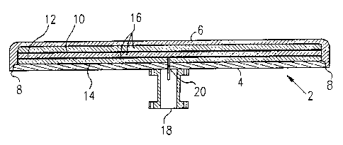
Figure 1 shows a cross-sectional view of a microwave antenna according to a
first
embodiment of the present invention. In figure 1 a flat plate antenna 2
comprises a mounting plate
4 and a box or radome 6, bonded together at a bonding surface 8. The mounting
plate 4 and radome
6 enclose a void in which is placed an antenna printed circuit board 12, a
polarises 10 and a
groundplane 14, separated by foam spacers 16. The PCB is connected to a
waveguide 18 via a
waveguide microstrip adapter 20. The waveguide microstrip adapter 20 serves as
a transition
between the output of the waveguide and the printed circuit board. Input to
the antenna may
alternatively be coaxial.
Figure 2 is an exploded diagram of the device shown in cross-section in figure
1.
As mentioned above, in the aperture coupled patch antenna the layers of PCB
with the various
active elements must be very carefully lined up and must be carefully spaced
apart. In order to
avoid radiation and surface wave losses in the printed patch array it is
necessary to keep the
6
CA 02250292 1999-04-13
spacings within the order of 0.01 ~,. Furthermore the narrow spacings mean
that the transmission
lines must be very thin. As they are thin the transmission lines will be lossy
and hence the antenna
inefficient for large arrays.
In embodiments of the invention the active elements, that is to say the
radiating elements and
the transmission lines, are all mounted on a single PCB. Both sides of the PCB
are used. The
manufacturing of the PCB is a very precise process. The thickness must be
tightly controlled and
the photolithography must be very accurately done. However assembly of the
antenna following
manufacture of the PCB does not require tight tolerances at all. The PCB 12
must be spaced
correctly with respect to the ground plane 14, but the spacing involved here,
of the order of a
quarter of a wavelength, is not critical.
The polariser, in addition to its having a polarizing function, is also
designed to reduce
radiation losses from the transmission lines.
Figure 3 shows a plan view of the printed, two-dimensional, surface of a PCB,
which
comprises an antenna element. The antenna element itself is a printed dipole
antenna. The array is
fed from the center 30. This form of feed is known as a corporate feed.
Transmission lines 32
branch outwardly from the center of the pattern, that is to say from the feed
point, and terminate in
radiating elements 34 at each termination of a transmission line. A corporate
feed has the
advantage that all lines are in phase and thus it achieves wide bandwidth. A
key feature of the
arrays used in the present invention is that, despite the fact that the path
to each radiating element
34 is identical in length, and that all elements are fed with equal
amplitudes, the antenna is able to
produce low side lobes and operate at high efficiency.
The radiating elements 34 preferably extend from the transmission lines 32 at
an angle of
substantially 45 degrees. The antenna may be used with these elements in the
vertical orientation,
as shown in figure 4. In this diamond orientation, vertical rows comprise a
decreasing number of
elements as one moves away from the center. Such an orientation is used to
decrease the size of
directional sidelobes, and at the same time allows each radiating element to
operate at substantially
the same power level. Previous attempts to improve side-lobe performance have
involved making
the transmission lines of different widths. This has the disadvantage that the
radiating elements
radiate at different power levels and, as a consequence are generally less
efficient.
7
CA 02250292 1999-04-13
Alternatively the antenna may be used with the radiating elements in a
horizontal direction.
In such an orientation the first side-lobes are just as low, <-25dB. The
antenna may be used
together with a polariser in order to improve the cross-polarization
performance, that is to say to
boost it to 30dB and beyond. The use of the polariser is optional and depends
on the particular
application.
It will be appreciated that, whether the radiating elements are positioned to
be horizontal or
vertical the antenna takes on the diamond shape of figure 4. It is possible to
put two or more such
diamond shapes together to make a composite antenna. Such a composite antenna
may be
advantageous in certain applications.
In an alternative embodiment the radiating elements are not at an angle of
45°. Instead,
straight elements are used, and this is done where low side lobes are not
required.
The array in figure 3 represents the array printed on one side of the PCB. On
the opposite
side of the PCB a complementary pattern is printed. The complementary pattern
relates to the first
pattern in that the respective transmission paths overlay one another. The
radiating elements of the
second pattern however, extend outwards from the terminations of the
transmission lines in the
opposite directions, at an angle of 180 degrees from the first radiating
elements. Figure 5 shows a
termination of a transmission element in which the two radiating elements 40
and 42, from the top
surface and the bottom surface respectively of the PCB, are shown
superimposed.
In general, the flat radiating elements 34 must be matched to the transmission
lines 32. The
_. transmission lines 32 must correspondingly be matched to the central feed
point 30. This is
achieved in the present invention as follows.
The flat element 34 has an impedance of typically 50 or 100 ohms. This element
is followed
by a transmission line 32 of the same impedance as the radiating element. The
transmission line 32
is then stepped up to 100 ohms. Two such transmission lines are connected
together via a T
junction. The common output yields 50 ohms. This is stepped up again
consecutively to 100 ohms
at the next T junction. This process is repeated right up to the central
input.
The impedance of the radiating elements must also be tightly controlled and
this is related to
the spacing between the respective PCB surfaces and the groundplane 14.
8
CA 02250292 1999-04-13
The total number of elements may range from 16 upwards, to 16,000 and beyond.
The bandwidth of the radiating element is independent of the dimensions of the
transmission
lines. This is because the radiating elements and the transmission lines use
separate ground planes.
In respect of the transmission lines the opposite face of the PCB serves as
the groundplane. The
separate groundplane 14 is for the radiation elements. It will be recalled
from the description of
figure 3 that the transmission lines of the two faces of the PCB overlay each
other. Hence the
opposite transmission line is able to serve as a groundplane in each case.
However the radiation
elements do not overlay each other and therefore the separate groundplane 14
is effective.
Flat patch array antennae of the prior art generally have bandwidths of around
1 to 4%.
Embodiments of the present invention can achieve bandwidths in the region of
20%. This
invention is particularly useful in large arrays where gain requirements are
greater than 32dBi. A
flatness of the gain peak of O.SdB over a wide band can generally be achieved.
A minimum cross-
polarization of 30dB can also be achieved.
Figures 6 and 7 show upper and lower layers respectively of a series parallel
feed for use in
embodiments of the present invention. The series parallel feed reduces losses
in the transmission
lines and thus improves efficiency. The series parallel array is
advantageously used when the
maximum bandwidth made available by the invention is not required.
Figure 8 shows a waveguide power divider for use with the present invention.
In a preferred
embodiment a number of arrays can be added together by means of a waveguide
power divider, and
figure 8 shows, by way of example, a 16-way divider. The power divider could
equally well be a
four way or a sixty-four way power divider depending on the particular
configuration. A problem
with PCBs is that, especially at high frequencies, large numbers of radiating
elements are needed.
To include each one of them on the same PCB requires a large PCB with long
transmission lines.
Transmission lines on a PCB are less efficient than waveguides. Thus it is
more efficient to have
several small PCBs connected by a waveguide power divider.
Fig. 9 shows an 8 by 8 point-to-point antenna. In order to deal with the
requirement that
sidelobes are kept extremely low the dipole elements 50 are balanced very
carefully. This may be
achieved by means of the curves 52 in the transmission lines linking the
dipole elements 50 to the
9
CA 02250292 1999-04-13
central stems 54. Additional curves 56 serve to reduce extraneous radiation
from the transmission
lines and again, these contribute significantly to sidelobe performance.
The feedpoint 58 contains a special pad designed so that soldering is only
required on one
side of the printed circuit.
Fig. 10 shows an LMDS subscriber antenna. This antenna again shows the use of
curves 52 in
the transmission lines to reduce radiation.
Fig 11 shows a base station antenna. This antenna is co~gured with a taper
arrangement to
yield a wide beam with a sharp skirt.
The antenna is sealed from the environment using the radome 6. In general
foamed plastic is
used in radomes and the reason is that, at the wavelengths at which the
antenna operates, materials
in general absorb energy from the radiation. Foamed plastic is less dense than
most materials and
therefore absorbs less energy, and it is a general object of the design of a
radome to minimize the
absorption of energy.
In the prior art the plastic used in the radome is foamed using a foaming
agent. The radome
has an inner body of foamed plastic, and an outer skin which need not be
foamed and which is
tougher than the body, to give the antenna an outer rigidity.
In embodiments of the present invention the radome is constructed of
polyolefin materials.
The materials may be laminated. The laminations are soldered together. The
material in the body is
typically foamed polyethylene and the material in the skin is typically the
more rigid polypropylene.
Polyethylene foam is typically an 80% cross-linked polymer and is manufactured
in a mold. The
laminations are obtained by peeling with an appropriate form of knife. The
fact that both the
materials are polyolefins makes the bond that much more secure.
Polypropylene, the more rigid of the two materials, and the one that is used
in the skin, is
vulnerable to UV damage from sunlight, and therefore it is advisable to cover
the radome with a
IJV mask, or to make it of a UV resistant polypropylene compound.
Advantages provided by embodiments of the invention may include the following:-
CA 02250292 1999-04-13
The spacing between the radiating element and the groundplane is independent
of the thickness of
the transmission lines or feed lines. In the prior art, the aperture fed
microstrip patch has complex
spacing and alignment requirements between adjacent elements. Such restriction
does not occur in
the invention.
The bandwidth of the radiating element is independent of radiation and surface
losses of the
feed lines. The bandwidth of the radiating element is a function of the
spacing between it and the
lower ground plane, which spacing defines about one quarter of the dielectric
wavelength.
A bandwidth of up to 20% is possible. The transmission lines are designed for
minimum loss
only. This is because radiation loss in the feed line is proportional to the
height of the PCB
substrate. The feed line can be designed with optimum substrate height and
thus losses can be
minimized. In the prior art, in which a single ground plane was used, this
cannot be done as
decreasing the height of the radiating element leads to a reduction in
bandwidth. Since two
groundplanes are now used it is possible to design the radiating element for
optimum bandwidth
(large gap to groundplane) and the transmission lines for minimum loss.(small
gap to groundplane)
Cross polarization is reduced considerably using a grid polariser. The
polariser is arranged to
be orthogonal to the polarization of the elements of the antenna.
The orientation of the array and the radiating elements reduces the size of
the directional
sidelobes.
' Complex distribution networks, of the type known in the prior art, are not
necessary, and
neither is accurate positioning between layers.