Note: Descriptions are shown in the official language in which they were submitted.
CA 02250336 2001-07-30
Specification
OPTICAL PULSE GENERATOR
Fif>Id of the Invention
The present invention relates to an optical pulse generator which stably
generates a
high cycling frequency optical pulse which is necessary for constructing very
high speed
communication systems.
Background Art
In recent years, optical fibers have: come to be widely used as a
communication path.
In .communication by optical fibers, transmission of large volumes of
information is possible.
At the present, with the development of multimedia and transmission of a
variety of
information as digital information on a world-wide scale, optical fibers have
come to be used
as 'the preferred communication path.
Thus, it is not difficult to imagine that the use of optical fibers as
communication
paths will flourish in the future.
One important factor when using optical fibers as a communication path is the
light
source, in particular, for example, the precision of a pulse light source. One
important factor
rel;~ted to the precision of the light sources is that the wavelength of the
light emitted does not
vary with changes in the environment (for example, changes in temperature,
etc.).
Summary of the Invention
In consideration of the above, an object of an aspect of the present invention
is to
provide an optical pulse generator which can generate an extremely stable high
cycling
frequency optical pulse train over a long period of time.
In order to obtain the above object, the present invention provides a laser
pulse
oscillator having in a ring an optical amplifying means having high gain in a
specified
wavelength band, a first optical path length regulator which performs high
precision optical
path length regulation, a second optical path length regulator which carries
optical path length
regulation over a wide range, an optical modulator which modulates incident
light and
converts it into an optical pulse, a clock signal extractor which converts the
laser optical pulse
emitted from said laser pulse generator into an electrical signal, and
extracts a clock signal of
an integral multiple of the cycling frequency of a
CA 02250336 1998-10-14
2
base frequency corresponding to the length of said loop, a frequency
difference detector
which detects the difference between a predetermined reference frequency
signal and
said clock signal, and a control means which controls the first optical path
length
regulator and the second optical path length regulator depending on the output
signal
from said frequency difference detector.
This invention obtains the effect that a very high cycling frequency optical
pulse train can be generated extremely stably over a long period of time
because the
length of a resonator of a laser oscillator is regulated by providing two
optical path
length regulators with differing characteristics, detecting with a frequency
voltage
converter the difference in frequency between a clock signal and a reference
frequency
signal obtained by converting an optical pulse into an electrical signal, and
supplying
the control signal to these two optical path length regulators which varies
according to
changes in the frequency difference.
In addition, the present invention is characterized in the second optical path
length regulator adjusting the optical path length by adding a temperature
change to an
optical pulse compression optical fiber.
In addition, the present invention is characterized in providing a high
precision
first frequency voltage converter which splits the output of the frequency
difference
detector and inputs one of the relevant outputs, a broad frequency band second
frequency voltage converter which inputs the other relevant output, a first
control means
which controls the first optical path length regulator according to the output
signal of
the first frequency voltage converter, and a second control means which
controls the
second optical path length regulator according to the output signal of the
first and
second frequency voltage converters.
In addition, the present invention is characterized in providing a central
control
means which detects the output signal to the first optical path length
regulator and the
output signal of the frequency difference detector, and controls the second
optical path
length regulator so that the control signal to the first optical path length
regulator does
not exceed a specified control limit.
In addition, the present invention is characterized in the central control
means
detecting the output signal of the frequency difference detector, and when the
frequency
detection range of the first frequency voltage converter is exceeded, causes
the output
signal of the frequency difference detector to return within the detection
range of the
first frequency voltage converter by controlling the first and second optical
path length
regulators.
In addition, the present invention is characterized by the central control
means
CA 02250336 1998-10-14
3
which recognizes the size relation between the frequency of the reference
frequency
signal and the clock signal by adding a change to the control signal to the
first optical
path length regulator and detecting the output signal of the frequency
difference detector,
and thereby controlling said second path length regulator.
Brief Description of the Drawings
Fig. 1 is a block diagram showing the structure of the optical pulse generator
according to the first embodiment of the present invention.
Fig. 2 is a block diagram showing the structure of the optical pulse generator
according to the second embodiment of the present invention.
Fig. 3 is a block diagram showing the structure of the optical pulse generator
according to the third embodiment of the present invention.
Fig. 4 is an explanatory diagram showing the relation between the output of
the
frequency difference between the reference frequency signal and the clock
signal, and
the frequency voltage converter.
Fig. 5 is a block diagram showing an example of the structure of an optical
pulse generator assumed in the present invention.
Detailed Description of the Preferred Embodiments
First, before explaining the embodiments of the present invention, the optical
pulse generator assumed in the present invention will be explained.
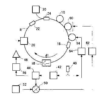
Fig. 5 is a block diagram showing an example of the structure of the optical
pulse generator assumed in the present invention.
As shown in Fig. 5, the optical pulse generator has a ring type resonator R.
This ring type resonator R connects in order a rare-earth doped optical fiber
10,
an optical pulse compression optical fiber 12, an optical path length
regulator 14, an
optical splitter 16, an optical isolator 18, an optical modulator 20, an
optical filter 22,
and an optical coupler 24.
The rare-earth doped optical fiber 10 is doped with a rare earth element such
as
erbium, excited by an external light source (light source 30, explained
below), and
radiates and amplifies the frequency of the light fixed by the doped element.
The optical pulse compression optical fiber 12 compresses the pulse range of
the incident optical pulse, and emits an optical pulse having a narrow pulse
band.
The optical path length regulator 14 is for regulating the optical path length
of
the ring resonator, and by regulating the optical path length of the ring type
resonator R
by this optical path length regulator 14, the conditions for resonation of the
ring
CA 02250336 1998-10-14
4
resonator are attained.
The optical splitter 16 is for extracting to the outside a part of the optical
pulses
circulating through the ring type resonator R. Because the pulse extracted out
of the
ring type resonator R by the optical splitter 16 are only optical pulses
having a phase
satisfying the resonation conditions of the ring type resonator R, the emitted
optical
pulses are a laser.
The isolator 18 fixes the circulation direction of the optical pulse in the
ring
type resonator R. That is, the optical pulse circulates in the direction of
reference
symbol dl in the figure, and because optical pulses propagating in a direction
opposite
to the direction shown by the reference symbol dl cannot transit the optical
isolator, the
optical pulses only circulate in the direction shown by the reference symbol
d1.
The optical modulator 20 is for carrying out intensity modulation of the light
circulating through the ring type resonator based the clock signal described
below, and
generating the optical pulse. The light emitted from the above-described rare-
earth
doped optical fiber 10 and not circulating through the ring type resonator R
does not
become optical pulses, and by being modulated by this optical modulator, is
converted
into an optical pulses.
The optical filter 22 has a specified pass bandwidth, has the characteristic
of
intercepting light of a frequency not includes in this pass bandwidth, and is
provided in
order to limit the wavelength of the generated optical pulse to within the
amplifier band
of the rare-earth doped optical fiber 10, and both eliminate spontaneously
emitted light
emitted from the above-described rare-earth doped optical fiber 10 and the
light of
unnecessary frequencies emitted from the excitation light source 30 described
below.
The optical coupler 24 is for guiding the excitation light emitted from the
excitation light source 30 to the ring type resonator R.
The excitation light source 30 is a light source for exciting the rare-earth
doped
optical fiber 10.
Reference numeral 40 in the figure is an optical splitter, and is connected to
the
optical splitter 16 in the ring type resonator, and is for splitting the
optical pulse emitted
from the ring type resonator R. One beam of the split optical pulses is used,
for
example, in a very high speed optical communication system.
The other beam of the optical pulses split by the optical sputter 40 is
incident
on the clock extractor 42.
The clock extractor 42 is for extracting the clock signal based on the
incident
optical pulse. This clock extractor 42 may comprise, for example, an optical
receiving
element which converts the incident optical pulse into an electrical signal,
and an
CA 02250336 1998-10-14
electrical amplifier which amplifies a narrow band filter and the output of
this narrow
band filter.
That is, the clock extractor 42 is for converting what is termed the incident
optical pulse into the clock signal of the electrical signal.
Reference numeral 44 is an electrical sputter, and splits the clock signal
emitted from the clock extractor 42, outputs one of the split off clock
signals to the
phase shifter 46, and sends the other signal to the frequency difference
detector 50.
The above phase shifter 46 is for regulating the phase of the input clock
signal.
The electrical amplifier 48 amplifies the clock signal output from the phase
shifter 46.
The clock signal output from the electrical amplifier 48 is input into the
optical
modulator 20 of the ring type resonator R.
Reference numeral 52 in Fig. 5 is a synthesizer which outputs a reference
frequency signal having a specified frequency. The above frequency difference
detector 50 detects a difference in frequency between the reference frequency
signal
output from the synthesizer 52 and the clock signal split off in the
electrical sputter 44,
and outputs this difference signal. This difference signal is output to the
control circuit
54.
The control circuit 54 outputs the control signal based on the input reference
signal to the optical path length regulator 14, and performs control which
regulates the
optical path length of the ring type resonator R.
In the above-described structure, the high cycling frequency optical impulse
is
generated in accordance with the following explanation.
When the excitation light is emitted from the excitation light source 30, it
is
incident on the ring type resonator R via the optical coupler 24. The
excitation light
which is incident on the ring type resonator R is propagated along the rare-
earth doped
optical diver 10, and excites the rare-earth doped optical fiber 10. Light of
a specified
wavelength is radiated from the excited rare-earth doped optical fiber 10.
This
radiated light is propagated along the ring type resonator R in the direction
shown by
the reference symbol d1 in the figure, and is incident on the optical
modulator 20 via the
optical pulse compression optical fiber 12, the optical path length regulator
14, the
optical sputter 16, and the optical isolator 18. When the light radiated from
the rare-
earth doped optical fiber 10 is incident on the optical modulator 20, it is
converted into
an intensity modulated optical pulse. The converted optical pulse is
propagated along
the ring type resonator R in the direction shown by the reference symbol d1 in
the figure,
and is incident on the rare-earth doped optical fiber 10 via the optical
filter 22 and the
optical coupler 24.
CA 02250336 1998-10-14
6
In the rare-earth doped optical fiber 10, because the excitation light is
incident
from the light source 30, the optical pulse which circulates one time through
the ring
type resonator R is amplified, and propagates along the ring type resonator R
in the
direction of the reference symbol dl. When this amplified light arrives at the
optical
modulator 20, it is pulsed, and the optical pulses are propagated along the
ring type
resonator R is the following manner.
While the above optical pulses are circulating along the ring type resonator
R,
one part of the circulating light pulse is split off by the optical sputter
16, and emitted to
the exterior of the ring type resonator R. The optical pulse emitted to the
exterior of
the ring type resonator R is split by the optical sputter 40, and one part of
the split off
light is used, for example, in a very high velocity communication system.
In addition, the other split off optical pulse is incident on the clock
extractor 42,
and an electrical clock signal is extracted. The extracted clock signal is
output to the
electric sputter 44.
One part of the split off clock signal is input into the phase shifter 46, the
phase
is adjusted, is amplified in the electric amplifier 48, and input into the
optical modulator
20. The optical modulator 20 intensity modulates laser light based on this
clock signal,
and outputs the optical pulse.
In addition, the other part of the split clock signal is output to the
frequency
difference detector 50, and in the frequency detector 50, the frequency
difference
between the reference frequency signal output from the synthesizer 52 and the
clock
signal split off in the electrical sputter is detected, and the difference
signal is output.
This difference signal is output to the control circuit 54, and based on this
input
difference signal, the control signal is output to the optical path length
regulator 14, and
the control for regulating the optical path length of the ring type resonator
R is carried
out.
Generally, if the resonator length (the physical length of the loop of the
ring
type resonator) is L, the refractive index of the optical fiber is n, and the
speed of light is
c, then the base frequency determined by the resonator length is:
fa=c/(nL).
Here, when the modulated frequency is set at a multiple q of the base
frequency, that is,
when:
qf"=qc/(nL),
(q being an integer), then by supplying the clock signal which agrees with the
multiple q
of the base signal to the optical modulator, the modulated frequency and the
cycling
frequency of the optical pulses agree, and high coherent mode synchronicity is
obtained.
CA 02250336 1998-10-14
7
Here, when only the temperature ~t of the optical fiber forming the ring type
resonator R is changed, only the length OL of the optical fiber changes, and
at the same
time, because the base frequency fo determined by the resonator length
changes, in
comparison with the modulated frequency f ( = q fo ) before the temperature
change,
only the fluctuation frequency 0f will deviate.
Of/f=OL/L=a0t .......... (1)
where L is the resonator length before the temperature change and a is the
coefficient of
linear expansion of the optical fiber. The fluctuation frequency Of of the
modulated
frequency is obtained by extracting one part of the clock signal extracted by
the clock
extractor 42 and detecting the frequency difference between it and the
synthesizer 52 by
the frequency difference detector 50, and the control circuit 54 controls the
optical path
length regulator 14 so that the fluctuation frequency Of of the modulated
frequency
disappears. By using this type of active negative feedback circuit which
automatically
adjusts the resonator length, the changing of the base frequency f~ along with
the
temperature fluctuation can be restrained, and the cycling frequency can
generate a
stable optical pulse train.
Moreover, the technology for this type of optical pulse generator is
disclosed,
for example, in Japanese Patent Application, First Publication, No. Hei 8-
18139.
However, in the above-described optical pulse generator assumed in the present
invention, in the optical path length regulator 14 the range within which the
resonator
length can be adjusted is limited. That is, when the control limit of the
resonator
length due to temperature change is exceeded, the fluctuation in the resonator
length due
to the temperature change cannot be completely restrained, and as a result,
the base
frequency fo varies with time.
As the above-described optical path length regulator 14, having a structure
wherein a tubular piezoelectric ceramic element is wrapped with an optical
fiber is used,
and by applying a control voltage to the tubular piezoelectric ceramic, the
wrapped
optical fiber expands, and the resonator length is adjusted. However, there is
a limit on
this adjustment range.
For example, the length which can be adjusted by the optical path length
regulator 14 is about 2 mm, and when the resonator length L = 200 m, f = 10
GHz, the
expansion coefficient a = 10'5, by the above Eq. 1, the differential frequency
Of = 100
kHz and the temperature change ~t = 1 ° C.
That is, if the temperature change of the optical fiber is not within
1° C, there is
the problem that an optical pulse chain with a stable cycling frequency cannot
be
generated.
CA 02250336 1998-10-14
8
In consideration of the above circumstances it is an object of the present
invention to provide an optical pulse generator which can very stably generate
over a
long period of time a high cycling frequency optical pulse.
Below, the optical pulse generator according to the embodiments of the present
invention will be explained in detail in reference to the drawings.
First Embodiment
First, the optical pulse generator of the first embodiment of the present
invention will be explained with reference to Fig. 1. Fig. 1 is a block
diagram showing
the construction of the optical pulse generator according to the first
embodiment of the
present invention.
In Fig. 1, the optical pulse generator has a ring type resonator R. This ring
type generator R connects in order a rare-earth doped optical fiber (the
optical
amplifying means) 10, an optical path length regulator (the second optical
path length
regulator) 60, an optical path length regulator (the first optical path length
regulator) 14,
an optical sputter 16, an optical isolator 18, an optical modulator 20, and
optical filter
22, and an optical coupler 24.
The rare-earth doped optical fiber 10 is doped with a rare-earth element such
as
erbium, is excited by an external light source (the light source 30 described
below), and
light of a wavelength determined by the dopant is radiated and amplified.
The optical path length regulator 14 is for adjusting the optical path length
of
the ring resonator, and the optical path length of the ring resonator R is
adjusted by this
optical path length regulator 14, thereby obtaining resonance conditions for
the ring
resonator.
In contrast to the optical path length regulator in Fig. 1 which can provide
high
precision optical path length control, the optical path length regulator 60
can provide
optical path length regulation over a wide range. That is, in the present
embodiment,
the most important point is being provided with two optical path length
regulators, the
optical path length regulator 14 which can control the optical path length
with high
precision, and the optical path length regulator 60 which can regulate the
optical path
over a wide range.
The optical sputter 16 is for extracting one part of the optical pulse
circulating
along the ring type resonator R to the outside. Because the optical pulses
extracted to
the outside of the ring type resonator R by the optical sputter 16 are the
only optical
pulses having a phase satisfying the resonance conditions of the ring type
resonator R,
the emitted optical pulses are laser light.
CA 02250336 1998-10-14
9
The optical isolator 18 determines the direction of circulation of the optical
pulse in the ring type resonator R. That is, the optical pulse circulates in
the direction
shown by the reference symbol dl in the figure, but because optical pulses
propagating
in a direction opposite to the direction shown by this reference symbol d1
cannot transit
the optical isolator 18, optical pulses can only circulate in the direction
shown by the
reference symbol d1.
The optical modulator 20 provides intensity modulation of the light
circulating
along the ring type resonator R based on the clock signal described below, and
is for
generating the optical pulse. Light which is emitted from the rare-earth doped
optical
fiber 10 described above and has not circulated one time around the ring type
modulator
20 has not become optical pulses, but is changed into optical pulses by being
modulated
by this optical modulator 20.
The optical filter 22 has a specified passing bandwidth, and the light with a
wavelength not encompasses within this passing bandwidth has the
characteristic of
being excluded, and in addition to restricting the wavelength of the generated
optical
pulses within the amplification band of the above-described rare-earth doped
optical
fiber 10, is provided in order that spontaneously emitted light emitted from
the above-
described rare-earth doped optical fiber 10 and unnecessary wavelengths of
light
emitted from the excitation light source 30 described below, are excluded.
The optical coupler 24 is for guiding the excitation light emitted from the
excitation light source 30 to the ring type resonator R.
This excitation light source 30 is a light source for exciting the rare-earth
doped optical fiber 10.
Reference numeral 40 in the figure is an optical splitter, is connected to the
optical splitter 16 in the ring type resonator R, and is for splitting off the
optical pulses
emitted from the ring-type resonator R. One part of the split off optical
pulses are used,
for example, in a very high speed communication system.
The other optical pulses split by the optical sputter 40 are incident on the
clock
extractor (clock signal extractor) 42.
The clock extractor 42 is for extracting a clock signal based on the incident
optical pulses. This clock extractor 42 comprises, for example, a light
receiving
element which converts the incident optical pulses into electric signals, and
an electric
amplifier which amplifies narrow band filter and the output of this narrow
band filter.
That is, the clock extractor 42 is for converting the incident optical pulses
into
electric clock signals.
Reference 44 is an electric sputter which splits off the clock signal output
from
CA 02250336 1998-10-14
the clock extractor 42, and outputs one part of the split off clock signal to
the phase
shifter 46, and the other part is split off to the frequency difference
detector 50.
The above-described phase shifter 46 is for adjusting the phase of the input
clock signal. The electrical amplifier 48 amplified the clock signal output
from the
phase shifter 46. The clock signal output from the electrical amplifier 48 is
input into
the optical modulator 20 of the ring type resonator R.
Reference numeral 52 in Fig. 5 is a synthesizer, and outputs a reference
frequency signal having a specified frequency. The above frequency difference
detector 50 detects the frequency difference between the reference frequency
signal
output from the synthesizer 52 and the clock signal split off by the
electrical sputter 44,
and outputs a difference signal. This difference signal is input to the
control circuit
(the first control means).
The control circuit 54 outputs to the optical path length regulator 14 a
control
signal based on the input difference signal, and carries out control for
adjusting the
optical path length of the ring type resonator R.
In addition, reference 62 in Fig. 1 is a control circuit (the second control
means) for carrying out control of the optical path length regulator 60.
Moreover, the control circuit 54 and the control circuit 62 are the control
means.
For example, when using as an optical path length regulator 14 a tubular
piezoelectric ceramic element wrapped with optical as used in conventional
technology,
the control range of the resonator length is about 2mm, the optical path
length L = 200
m, f = 10 GHz, and the linear expansion coefficient a = 10''5, by the above-
described Eq.
1, Of = 100 kHz and 0t = 1° C. That is, when there is fluctuation of
100 kHz or greater
of the cycling frequency due to external factors such as temperature, an
optical path
length regulator 60 is necessary.
Now the optical path length regulator 60 will be explained. If the length of
the resonator described above (the length of the loop of the ring type
resonator R) is L,
the refractive index of the optical fiber is n (about 1.48), the speed of
light is c (about 3
x 10~m / sec), then the base frequency determined by the resonator length L,
fo = c / ( n
L ), is 1 MHz. That is, in the present embodiment, a pulse resonating mode
exists at f
= 10 GHz at about a 1 MHz interval. If the adjustment range of the optical
path length
regulator 60 is 1 MHz or greater, it is possible to carry out control so as to
arbitrarily set
the cycling frequency at the f = 10 GHz band.
From the above, it is a necessary condition that the optical path length
regulator
60 has a wider optical path length adjustment range than the optical path
length
CA 02250336 1998-10-14
11
regulator 14, and it is preferable that it have an adjustment range for the
resonant length
corresponding to the base frequency.
Second Embodiment
Next, the optical pulse generator according to the second embodiment of the
present invention will be explained.
The optical pulse generator according to the second embodiment of the present
invention has almost the same construction as the optical pulse generator
according to
the first embodiment shown in Fig. 1, but differs on the point that the
optical path length
regulator 60 adjusts the optical path length by providing a temperature
adjustment on to
an optical pulse compression optical fiber.
An optical pulse compression optical fiber, such as that disclosed in Japanese
Patent Application, First Publication, Number Hei 8-18139, is provided in a
ring type
resonator in order to generate optical pulses with short pulse widths by using
the optical
soliton effect. In the conventional optical pulse generator explained
referring to Fig. 5
as well, an optical pulse compression optical fiber 12 is used in a ring type
resonator.
Here, the largest part of the resonator length of the ring type resonator is
made
up of the optical pulse compression optical fiber 12, and when the resonator
length L =
200 m, the modulation frequency fluctuation Of = 1 MHz, and the modulation
frequency
f before fluctuation is 10 GHz, then from Eq. 1 described above, the change in
the
length OL of the optical pulse compression optical fiber is 20 mm and the
fluctuation in
temperature Ot is ~L ~t = 10° C. That is, by using a 200 m optical
pulse compression
optical fiber on the optical path length regulator 60 in Fig. 1, and
maintaining it within a
range of 10° C, the following width of the fluctuation of the cycling
frequency is greatly
widened, and in addition, the it is possible to set and control the cycling
frequency at an
arbitrary frequency in the 10 GHz band, and generate a very stable optical
pulse train
over a long period of time.
Third Embodiment
Next, the optical pulse generator according to the third embodiment of the
present invention will be explained referring to Fig. 2. Fig. 2 is a block
diagram
showing the structure of an optical pulse generator according to the third
embodiment of
the present invention. The same reference symbols denote the same parts of the
optical pulse generator according to the first embodiment of the present
invention
shown in Fig. l, and their explanations are omitted.
The optical pulse generator according to the third embodiment of the present
CA 02250336 1998-10-14
12
invention shown in Fig. 2 differs from the optical pulse generator according
to the first
embodiment of the present invention in having provided, between a frequency
voltage
converter (a first frequency voltage converter) 70 and a frequency voltage
converter (a
second frequency voltage converter) 72, the frequency difference detector 50,
the
control circuit 54, and the control circuit 62.
In the present embodiment, the optical path length regulator 14 and the
optical
path length regulator 60 are controlled by detecting the frequency difference
between
the reference frequency output from the synthesizer 52 and the clock signal,
and in
order to control the optical path length regulator 14 which can control the
optical path
length with high precision, it is necessary to provide a frequency voltage
converter 70
which can detect the frequency difference with high precision, and in order to
control
the optical path length regulator 60 which can control the optical path length
over a
wide range, it is necessary to provide a frequency voltage converter 72 which
can detect
frequency differences over a wide range. Therefore, the most important point
of the
present embodiment is the point that the frequency voltage converters 70 and
72 cannot
be used together and are provided as separate units.
As described above, the frequency control range of the optical path length
regulator 14 is 100 kHz, but in order to perform frequency control with higher
accuracy,
it is necessary to increase the precision of the error detection.
For example, a representative frequency voltage converter has an full-scale
output voltage of 10 V, and in addition, if in the usual electrical circuit it
is difficult to
accurately detect a voltage of lm V or less, when it is desired to obtain a
frequency
difference detection precision of 1 Hz, it is necessary to make the input
frequency of the
frequency voltage converter 70 10 kHz or less.
In addition, the frequency control range of the optical path length regulator
60
is 1 MHz, and a frequency voltage converter 72 which can detect a frequency
difference
in all frequencies in the control range is necessary. Here, when the frequency
difference between the reference frequency signal and the clock signal is
small, the
optical path length regulator 60 can be controlled by the output signal of the
frequency
voltage converter 70.
In the present embodiment, a frequency voltage converter 70 and a frequency
voltage converter 72 having a differing frequency detection range are used,
and the
optical path length regulator 14 is controlled by the output signal from the
frequency
voltage converter 70, and the optical path length regulator 60 is controlled
by the output
signal from the frequency voltage converter 70 or the frequency voltage
converter 72.
CA 02250336 1998-10-14
13
Fourth Embodiment
Next the fourth embodiment of the present invention will be explained in
reference to Fig. 3. Fig. 3 is a block diagram showing the structure of the
optical pulse
generator according to the fourth embodiment of the present invention, and the
same
reference symbols denote the same parts of the optical pulse generator
according to the
third embodiment of the present invention shown in Fig. 2, and their
explanation is
omitted.
The optical pulse generator according to the fourth embodiment of the present
invention shown in Fig. 3 and the optical pulse generator according to the
third
embodiment shown in Fig. 2 differ on the point between the frequency voltage
converter 70, the frequency voltage converter 72, and the control circuits 54
and 62 a
microprocessor (central control means) 80 is provided.
In the explanation of the above-described first through third embodiments,
the limit of the control range of the optical path length regulator 14 was
described. In
the third embodiment, a method of separate control of the optical path length
regulator
14 and the optical path length regulator 60 is disclosed.
However, it is unclear where in the control range of the optical path length
regulator 14 is positioned, and provisionally when the limit of the control
range is
exceeded high precision control of the frequency becomes impossible. That is,
because it is unclear to what degree the optical path length regulator 14 can
control the
length of the loop of the ring type resonator R in the direction of
lengthening, or to what
degree it can control the length of the loop in the direction of shortening,
high precision
control when the limit of the control range is exceeded becomes impossible.
In the fourth embodiment of the present invention, the control voltage to the
optical path length regulator 14 and the output voltage of the frequency
voltage
converters 70 and 72 is detected by a microprocessor 80, and the control
circuit 62 of
the optical path length regulator 60 is controlled so that the optical path
length regulator
14 does not exceed the limit of the control range. In this manner, the optical
path
length regulator 14 does not exceed the limit of the control range, and high
precession
frequency control is always possible.
Fifth Embodiment
Next, the fifth embodiment of the present invention will be explained. The
structure of the optical pulse generator according to the fifth embodiment of
the present
invention is roughly similar to the optical pulse generator according to the
fourth
embodiment shown in Fig. 3.
CA 02250336 1998-10-14
14
The fifth embodiment of the present invention is for controlling the frequency
difference detected by the frequency difference detector 44 when it is below
the
detection range of the frequency voltage converter 70.
In explaining the third embodiment of the present invention, there existed a
mode at the cycling frequency f = 10 GHz wherein the pulse oscillated at about
a 1
MHz interval. For high precision frequency control, the frequency difference
between
the reference frequency signal output from the synthesizer 52 and the clock
signal
output from the clock extractor 42 must be equal to or less than the detection
range of
the frequency voltage converter 70. The detection range of the frequency
voltage
converter 70 is, for example, 10 kHz or less.
In the fifth embodiment of the present invention, the output voltage of the
frequency voltage converters 70 and 72 are detected by the microprocessor 80,
and the
control circuits 54 and 62 of the optical path length regulators 14 and 70 are
controlled
so that the frequency difference between the reference frequency signal and
the clock
signal lies within the detection range of the frequency voltage converter 70.
Here, if the frequency difference between the reference frequency signal and
the clock signal is equal to or less than 1 MHz, detection of the frequency
difference by
the frequency voltage converter 72 is possible, and when the frequency
difference is
large, the optical circuit 62 of the optical path length regulator 72 is
controlled. In
addition, if the frequency difference between the reference frequency signal
and the
clock signal is, for example, 10 kHz, and is in a range which can be
sufficiently
controlled by the optical path length regulator 60, then the control circuit
54 of the
optical path length regulator 14 is controlled.
Sixth embodiment
Next, the optical pulse generator according to the sixth embodiment of the
present invention will be explained. The structure of the optical pulse
generator
according to the sixth embodiment of the present invention is roughly similar
to the
optical pulse generator according to the fourth embodiment shown in Fig. 3.
The sixth embodiment of the present invention is for control of the optical
path
length regulator 60 after the frequency difference detected by the frequency
difference
detector 44 falls below the detection range of the frequency voltage converter
70.
In the fifth embodiment described above when the frequency difference
between the reference frequency signal and the clock signal was large, the
control
circuit 62 of the optical path length regulator 60 is controlled.
Here, the frequency difference detector 50 outputs only the frequency of the
CA 02250336 1998-10-14
frequency difference between the reference frequency signal and the clock
signal, and
does not output information on their size relation. In addition, the detection
of this
frequency difference is performed by the frequency voltage converter 72, but
usually
the output of the frequency voltage converter generates the output voltage
proportional
to the input frequency.
When the frequency control is by controlling the optical path length regulator
60, it is necessary to detect the size relationship between the frequencies of
the
reference frequency signal and the clock signal.
Fig. 4 is a drawing for explaining the relationship of the output of the
difference frequency between the reference frequency signal and the clock
signal, and
the output of the frequency voltage converter 72. When the difference
frequency
between the reference frequency signal and the clock signal is 0 f,, + 4 fl
and - ~ f, are
the symbols that carry the information concerning the size relationship
between the
reference frequency signal and the clock signal.
In either the case of + 0 f, or - 0 f,, the output of the frequency voltage
converter is Vl.
Here, when the difference frequency of the frequency between the reference
frequency signal and the clock signal is 4 fl, when the frequency of the clock
signal is
changed only + 0 f, by controlling the optical path length regulator 14, the
difference
frequency is + 0 fl+ 0 fz or - 0 f,+ ~ fl, and the output of the frequency
voltage
converter 72 is VZ or V3. By detecting the behavior at this time, the size
relationship of
the frequencies of the reference frequency signal and the clock signal can be
recognized.
In the sixth embodiment of the present invention, the frequency of the clock
signal is changed by controlling the optical path length regulator 14, and the
output of
the frequency voltage converter 72 at this time is detected by a
microprocessor 80, and
thereby the size relationship of the frequencies of the reference frequency
signal and the
clock signal can be detected, and the control circuit of the optical path
length regulator
60 can be controlled according to the result of this detection.