Note: Descriptions are shown in the official language in which they were submitted.
CA 022~0912 1998-10-01
Text as amended under PCT ChaPter ll
ENT1 E001 WO/ws9801 52/Dr. L./bz131 .08.1998
Electronic card for electromaqnetic data exchanqe and a Process for manu-
facturino such a card
Description
The invention relates to an electronic card for electromagnetic data exchange,
the electronic card having an electronic circuit, which is contained in a housing,
as well as process for manufacturing such a card.
Electronic cards with an imple",e,)led electronic circuit are already known and are
10 used, for example, as telephone cards, as credit cards with an integrated tele-
phone card function, etc. In these cases, the electronic circuit is contained in an
hermetically-encapsulated casing and is placed upon a suppo, lil ,9 element of the
electronic card. The disadvantage of this procedure is that it can be carried out
only at rather high costs, since the encapsulating of the microchip is difficult to
15 carry out, due to the temperature sensitivity of its electronic col"ponents.
Nowadays such electronic cards are used not only for the above-mentioned func-
tions, but they are also used as so-called lra"s~.onder cards, such as electronic
cards for a radio-frequency identification system for tracing luggage, for example.
Here the el~lron,c circuit consists of an antenna element and an evaluation unit20 connected to the anlenna element via thin wires. Due to its spatial extension,
such an electronic circuit can no longer be encaps~ by a simple plastics in-
jection moulding process - like a microchip for example -, since the wires connect-
ing the antenna element and the evaluating unit of the electronic circuit would be
da",aged due to the pressure resulting from the injection moulding process.
25 There~re, at present the electronic circuit has to be sealed via a la",inaling
CA 022~0912 1998-10-01
process, carried out at a temperature of 130~ for 20 to 30 minutes. The disadvan-
tage of using such a pr~ure is that the necessary working te~n~erat.Jre for the
electronic card circuit generally reaches the limits of technological feasibility, so
that during the present production of such an electronic cards a high failure rate
5 is ex~ ed.
It must be clarified that the above-mentioned cards are cards which are neither
electronic cards such as are used with personal computers for example, nor elec-tronic cards whose casing already conslilutes the final casing for the electronic
card.
10 It is the object of the invention to develop a housing for an electronic circuit of an
electronic card, which is easy to produce and which yields a proper protection for
the electronic circuit co"lained within.
This object is acl lia~Aed according to the invention in that the housing is provided
with a bottom element and a top element, in that the eJectronic circuit is contain~J
15 between the inner surfaces of these two ele",ents, that at least one of the bottom
element and the top element is provided with at least one recess, into which theelectronic circuit is ins~, led, that the shape of the recess co" esponds to the outer
shape of the clect~onic circuit, that the ele~l, onic circuit is at least partially cov-
ered by the top element, and that the housing is encased by a sheating made of
20 plastics.
A housing for the el~,onic circuit of an cl~ctro,lic card is created in an advanta-
geous manner by the procedures according to the invention and this housing can
be produced via a simple plastics injection moulding process in a convenient way.
The recesses accord;ng to the invention, provided at least within the bottom ele-
25 ment of the housing, make it advantageously possible to incol~,orate even spa-
tially extended electronic circuits, which are contained within the housing, safe
CA 022~0912 1998-10-01
and protect~l form outer t~"p~ratures after the top element has been placed
upon the bottom element and the two ele",ents have been cGnnecled if required.
Sl ~hseg~lently in order to produce the actual electronic card the housing accord-
ing to the invention can be placed ~ogetl ,er with the ele~(, unic circuit protec l~J
5 from ,nechanical andlor ll,~mal influences into a plastics injection moulding ma-
chine and the injection moulding process can then be car~ icd out.
An advantageous further development of the invention provides that at least one
of the bottom element and the top element of the housing according to the inven-tion are provided with at least two spatially separate recesses for receiving two
10 separate coi~")onents of the el~1,unic circuit whereby these two recesses areconnecled via at least one recess for receiving wires connecting the two above-
mentioned con"~nei,ls. Such a design has the advantage that in this way even
electronic circuits c~nsisling of several spatially separdle co",poi,ents can becontained in a convenient manner within the housing according to the invention
15 prùt~tecl from mechanical and/or ~I,e"nal influences.
Another advantageous development of the invention provides that one of the two
recesses provided serves to receive an anle.,na element and the other recess
serves to receive an evaluation unit of the electronic circuit. This design is par-
ticularly suitable for an el~onic card that is to be used as a radio-frequency
20 identification system.
In an advanPgeous further development of the invention the housing is made of
an elastic material. Thus a flexible construction of the electronic card is obtained
in a convenient manner.
Further advant~geous developments of the invention are the subject of the de-
25 pending claims.
CA 022~0912 1998-10-01
Further details and advantages of the invention can be noted from the exemplary
enl~c;;.,~, ItS which are descri~ed below by means of the figures:
Fig. 1 shows a first exemplary e",bodi."ent of a housing for the ele 1,onic
circuit of an electronic card
Fig. 2 shows a second exemplary embodiment of a housing for the elec-
tronic circuit of an electronic card and
Fig. 3 shows an electronic card constructed from the housing of Fig. 2.
The exemplary embodiment of Fig. 1 re~.rasenling a housing 1 for receiving an
electronic circuit 2 (shown here merely schematically and in a dotted line) mainly
10 consisls of a bottom element 10 and a top element 20 which are connected via
connecting elements 31 a 31 b in such a way that top element 20 can be folded
over onto the bottom element 10 so that the inner surface 10 of the bottom ele-
ment 10 comes into conLa..t with the inner surface 20' of the top element 20. Itmust be noted here that although it is convenient to cGnnect the bottom element
15 10 and the top element 20 via the conne~ling ele",e"ts 31a 31b it is also possi-
ble to omit these cGnne~ing elements 31 a 31 b so that the housing 1 then con-
sists of two separate parts 10 20.
The bottom element 10 of the housing 1 is basically ret~ang.Jlar its shape limited
by longitudinal edges 1 Oa and 1 Ob and by cross edges 1 Oc and 1 Od. Here the
20 size of the bottom element 10 is somewhat smaller than the size of an electronic
card using the already described housing 1. The bottom element 10 is provided
with two recesses 11 and 12 serving to receive a first antenna element 2a and a
,
CA 022~0912 1998-10-01
second anten.,a ele",ent 2b rt:spe~ /ely of the electronic circuit 2. The bottomelement 10 is further provided with an opening 13 for a microchip 2c which is be~Gcessible from the surface of the electronic card. As it can be seen from Fig. 1
the shapes 1 1 12 of the recesses 1 1 12 and the shape 13 of the opei ,ing 13
5 cones~,ond to the outer shapes 2a' 2b 2c of the resp~live co""~onents 2a 2b
2c of the electronic circuit 2 so that these components 2a - 2c of the el~, u"iccircuit 2 are essentially contained in a fixed position within the bottom element 10
of the casing device 1.
The top element 20 of the casing device 1 is shaped in such a way that when the
10 top element 20 is folded via the connecting elements 31 a 31 b onto the bottom
element 10 those areas of the electronic circuit 2 to be protected from ~l~echani-
cal and/or thermal influences are covered by the top element 20. Thus the top
element 20 is provided with a further recess 21 cooperating with the recess 11 of
the bottom element 10 as well as with one further recess 22 cooperating with the15 recess 12 of the bottom element 10 both recesses are positioned at least par-tially above the ~cesses 11 or 12 respectively when the housing 1 is in its as-
sembled state. It is now assumed for the purpose of illustration only that the
electronic circuit 2 does not require that the right part (as shown in ~ig. 1 ) of the
first anlenna element 2a contained within the recess 11 is to be protected from
20 therrrlal and/or mechanical influences by the top element 20. Th~ ore the upper
are a of the top element 20 does not extend over the entire width b of the anten"a
element 2a but is sl ,o, lened in this direction. In the same way assuming that the
lower part of the second antenna element 2b when conlained in the recess 12
does not have to be pr~,t~ed from the above-mentioned influences the top ele-
2~ ment 20 is designed in such a way that is does not cover the lower area of thesecond ante~"~a element 2b of the elect,onic circuit 2.
In a co"espondi"g way the top element 20 of the housing 1 is provided with an
opening 23 for the i"icrochip 2c of the electronic circuit. In order to be able to
conlain the connecting wires 2d whose diameter is typically 6/100 mm and which
CA 02250912 1998-10-01
-6 -
serve to connect the elect~onic compor,ents 2a - 2c of the eleclronic circuit 2,within the housing 1, prot~e l from heat and tea, ing, the top element 20 - as
shown in Fig. 1 - is provided with recesses 24a, 24b for the con"eoting wires 2dwhich connect the opening 23 with the recesses 21, 22. It should be noted here
5 that it is also possible to provide these recesses 24a, 24b within the bottom ele-
ment 10 of the housing 1 as well, and that in this case it is eventually possible to
omit the recesses 24a, 24b of the top element 20 of the housing 1. It is furtherpossible to use a foil instead of the connecting wires 2d.
From the above description the skilled person can see that in the top element as10 well, the design and arral ,ger"ent of the recesses 21, 22 and of the opening 23
CGI I espond to the outer shapes 2a', 2b', 2c' of the electronic cG",ponents 2a - 2c
of the electronic circuit 2 which is to be contained within an inner space of the
housing 1, this inner space being limited by the inner surfaces 10' and 20' of ele-
ments 10, 20. It is i,~po,lan~ here only that these recesses 11, 12 and 21, 22 re-
15 spectively and ope"ings 13, 23 respectively are designed in such a way that theelectronic co",~nenls 2a - 2c of the ole~,1lullic circuit 2 can bs contained within
the above-mentionsd recesses and openings in a way that sufficiently protects
them from mschanical and/or thermal damage.
The above~es~ ibsd construction has the advantage that the housing 1 can be
20 prsduced in an easy-to-carry out step of operation via a plastics injsction-
moulding process, whsreby an elastic plastic material can conveniently bs used
for producing the housing 1. It is howsver possibl~ to use a rigid plastic material
as well for producing the housing 1.
After the housing 1 has bssn designsd as described above, ths cG",ponenls 2a -
25 2d of the electronic circuit 2 are inserted into recesses 11, 12 of the bottom ele-
ment 10. The top element 20 is then folded via the connecting ele",e"(s 31a, 31bonto the bottom element 10, whereby the connecting wires 2d are received within
the recesses 24a, 24b of the top element 20. After that, the bottom element 10 is
.
CA 022~0912 1998-10-01
connected to the top element 20 at least at pre-dete, ~ eJ points - preferably by
means of bonding engaging via not~l ,es clamping or weldil ,~ - so that the top
element 20 is firmly fixed onto the bottom element 10. In this way a safety feature
for trans~, l pUI ~oses is created for the electronic circuit 2 as well which pre-
5 vents the electronic circuit 2 from becoi"ing detached during handling ortransport.
The entity created in this way is then placed into a plastics injection-moulding ma-
chine and is encased via a plastics injection moulding process in order to create
the actual ready-to-use electronic card whereby the non-sensitive areas of the
10 electronic c~",,l~onents 2a - 2d which are not covered by the top element 20 are
now encase~J by sheathi"g.
The above-described housing 1 for receiving the electronic circuit 2 of the elec-
tronic card excells by the fact that the housing 1 containing and protecting theelectronic circuit 2 can be produced simply and thus inexpensively via a plastics
15 injection-moulding p(ocess. In addition it is possible to produce flexible electronic
cards in this way.
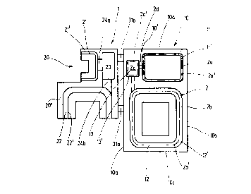
Fig. 2 shows a second exemplary embodiment of a housing 1 the basis con-
struction of which corresponds to that of housing 1 shown in Fig. 1 so that the
same and co" esp~nding parts may be marked with the same reference numbers
20 and need not be described in detail again.
One of the dirrerences between housing 1 and housing 1 lies in the fact that thebottom element 10 and the top ele",e"t 20 are essentially of the same size i.e.
that the top element 20 when folded over onto the bottom ele "ent 10 essenliallycovers the bottom element 10 entirely. The expert can see clearly that such a dif-
25 ference between the bottom and top elements 10 20 of the two embodimenlsrepresents an optionally difrere"t variation of the construction principle of the first
exe,llplary e",bodi",ent.
CA 022~0912 1998-10-01
Fulltlen~,ore in the case of housing 1 the bottom ele "enl 10 and the top ele-
ment 20 are no longer conne-ted via two connecting ele,nenls 31 a 31 b but via
three connecting ele"~e, lts 31 a 31 b 31 c. This is merely anotl ,er way of many dif-
ferent ways in which the bottom elen,ent 10 can be cor"~e~ed with the top ele-
5 ment 20. With regards to housing 1' it is of course possible as well to omit theconnecting element 31 a 31 c so that the housing 1 then consists of the separale
parts 10 20.
The bottom element 10 of housing 1 is provided with two recesses 11 a and 12a
correspo"d; ,g to the recesses 11 and 12 of housing 1 whereby recess 11 a now
10 serves to receive the ~lliC~O~lip 2c (cf. Fig. 3) and recess 12a serves to receive
the anl~nna element 2a. As can be seen clearly from Fig. 2 and Fig 3 the shapes
11 a and 12a of recesses 11 a 12a co"espGnd to the shapes 2a 2c of the re-
spective colllponenls 2a 2c of the ele.~,onic circuit 2 so that for the housing 1
these COillpGI ,ents 2a 2c of the ele~:ll onics circuit 2 are essentially contained in a
15 fixed position within the bottom element 10 of housing 1.
In the same way as for housing 1 the top element 20 of the housing 1' is pro-
vided with a further recess 21 a cooperali"g with the recess 11 a of the bottom ele-
ment 20 as well as with one further recess 22a cooperatin~ with recess 12a of
the bottom element 10. These recesses 21a 22a are positioned above recesses
20 11 and 12a respecti~ely when the housing 1 is in its assefi,bled state.
Like in housing 1 in housing 1 the microchip 2c co"tained within recess 11 a is
protected from lhe""al and/or n,ecl,anical irfluences by the top element 20. Theupper area of the top ele "ent 20 of housing 1 - unlike that of housing 1 shown in
Fig. 1 - ll ,erefore extends here over the entire width b of the top element 20. In a
25 corresponding ",ar,ner the antenna eleine"~ 2a contained within recess 12a isfully covered by the top element 20 so as to protect the antenna element 2a frommechanical and/or thermal influences.
.
CA 022~0912 1998-10-01
As it can be seen from Fig. 2 in order to obtain a better adjusl",ent of the recess
21a to the cG",ponent 2c to be received ll,erei~ recess 21a of the top element 20
of the housing 1 is provided with recesses 25a - 25d for the purpose of better ad-
ju:~lrne,lt of recess 21a to the structure of the i".~ ,ip 2c to be received therein.
5 It can be further seen from Fig. 2 that the bottom element 10 is provided with two
clamp ele,ne,lts 29a 29b for connecting wires 2d (not shown in Fig. 2) which
serve to connect the microcl ,ip contained within the recess 11 a and the a"lenna
ele."ent 2a contained within the recess 12a. 8y means of these clamp elements
29a 29b the conneoting wires 2d are pushed against the top element 20 of the
10 housing 1 and are thus held in place. It is also possi'~lc however that one or
both clamp e,l&, nen~s 29a 29b are arranged at the top element 20.
Another di~erence between the two embodi-,~ents is the fact that the housing 1 is
provided with an opening 40 a~,dnged essenlially in the centre of its top element
20 which is positioned above an recess 41 of the bottom element 10 when the
15 housing 1 is folded over. Two channels 42a 42b within the bottom element 10 ex-
tend from recess 41 to the edge 10c of the bottom element 10. They are covered
by correspo"ding covers 43a 43b within the top element 20 when the housing 1
is folded over. Of course it is also possible as an all~r"dti~e to provide the open-
ing 40 within the bottom element 10 and to andnge the con,~onents 41a 42a
20 42b within the top ~le.llenl 20 of the housing 1.
The opening 40 within the top ele."ellt 20 as well as the ~,a"nels 42a 42b within
the bottom element 10 serve for the purpose of producing from the centre of the
housing 1 the sheathing 50 seen in Fig. 3 of the housing 1 for the manufactur-
ing of the actual card. This is done by placing the housing 1 in its folded-over25 state whereby the components 2a 2c to be prolecled by the housing 1 are con-
tained with the housing 1 and are covered by the bottom element 10 and the top
element 20 into a plastics injection-moulding ",achine in such a way that a
., . . .. _ .
CA 022~0912 1998-10-01
- 10 -
narrow free space remains along the circu"~erence of the housing 1'. The
injection-moulding "~aterial is then conveyed via the opening 40 into the cl~annels
42a, 42b and p~sses through these char" l~ls 42a, 42b to their outlet openings
42a', 42b', thereafter encasing the housing 1 in order to produce the actual elec-
5 tronic card, whereby the injection moulding ll,alerial flows along the outer edge ofthe housing 1', thus forming the seamless sheathing 50. The advantage of such a
procedure is the fact that the surface of the housing 1' can be hermetically
sealed. In addition, there is advantageously no breakage of the housing 1' when
bending stresses occur.