Note: Descriptions are shown in the official language in which they were submitted.
CA 02250968 1998-10-02
WO 98/34411 PCT/HU98/00012
Method and apparatus for displaying three-dimensional images
Technical Field
The invention relates to a method and apparatus for displaying three-
dimensional images, in particular moving images based on video signals con-
taining three-dimensional image information. The invention may be used in all
fields of displaying images.
When a planar image is produced on a surface, the light emitted or reflected
from each point of the surface in any direction has approximately the same in-
tensity (and colour). This is the working principle of a written sheet, of
paper
(based on reflection) or a traditional television image (based on emission).
But
displaying a spatial image, the light emitted from a point of the surface in
dif-
ferent directions have different intensity (and colour). This is the working
prin-
ciple of a window-pane regarded as a "display", or that of a hologram. In
short,
for producing spatial images there is needed a light emitting surface, where
the
intensity (and colour) of the light emitted from a point of the picture, i. e.
a
pixel. may be controlled, depending on the exit angle, that is, the intensity
of
the light may be controlled in the different emitting directions.
Background Art
Solutions to produce spatial images with laser technology, such as holograms,
stereograms, etc. are known. It is a shortcoming of the known laser systems
that
they are inadequate for producing three-dimensional images from video signals.
A method and apparatus for producing three-dimensional pictures is known
from the International Patent Application published under WO 94/23541. This
specification discloses two basic methods for producing three-dimensional im-
ages.
According to a first version of this known solution, the modulated laser beams
SUBSTITUTE SHEET (RULE 26)
CA 02250968 1998-10-02
WO 98/34411 PCT/HL198/00012
-2-
are subjected to deflection according to the directions defining a field of
view,
and controlled in time, so that the modulated laser beam impinges on a prede-
termined pixel deflected, with a given entry angle, or parallel displaced, and
exits from the pixel deflected or without further deflection, according to a
pre-
y determined direction defining the field of view. A disadvantage of this
solution
is that the laser beam needs very precise focusing and positioning, because
the
direction of the exiting laser beam is determined by the entry point within
the
pixel.
According to the other version, the modulated laser beam arrives at the pixel
without any deflection within the entry points, and the time-resolved
deflection,
dependent of view directions is effected with controllable active optical ele-
ments, placed in each pixel. The angle deflection, dependent of the intensity,
is
performed by the active optical element. An advantage of this solution is that
less precise focusing and positioning is needed, but a further disadvantage is
that the active optical elements make the apparatus very expensive.
Hence it is an object of the invention to provide a method and apparatus for
producing three-dimensional images, enabling to produce three-dimensional
images using video signals containing three-dimensional image information.
and this without the need for using expensive focusing and positioning ele
ments. It is a further object of the invention to provide a method and
apparatus
for producing three-dimensional images, where a high-resolution screen does
not contain expensive active beam deflecting elements, and which may be
manufactured economically.
Disclosure of the Invention
To achieve the above mentioned goals, we have found that a method for pro-
ducing a three-dimensional image, comprising the steps of:
simultaneously modulating a - preferably spatially coherent - light beam by a
video signal containing three-dimensional image information; and
directing the modulated light beam to pixels (image points) defining a first
light
emitting surface;
SUBSTITUTE SHEET (RULE 26)
CA 02250968 1998-10-02
WO 98/34411 PCT/AU98/00012
-3-
emitting a component of the light beam from the pixels within a predetermined
angle of view (field of view) in the different view directions, with an
intensity
corresponding to the three-dimensional image,
directing the modulated light beams to the pixels from different entry angles,
depending on the emitting angles within the angle of view, would provide a
good basis for the invention.
According to the invention, this method should include directing the light
beams modulated corresponding to the different directions to the pixels of the
first light emitting surface from one or more light emitting points of a
second
light emitting surface, said second light emitting surface being spaced apart
with a predetermined distance from the first light emitting surface.
Essentially, with this solution the functions of the first light emitting
surface,
practically the screen, are separated, and only the horizontal deflection and
the
vel-tical dispersion or divergence is performed on the first light emitting
sur-
face, while the light beams necessary for the creation of the image are
produced
and controlled at the second light emitting surface.
A prefen-ed version of the method according to the invention includes
selecting
the number of the light emitting points and the number of light beams (the an-
gle resolution) emitted therefrom in such a manner, that their product is
equal to
the product of the number of pixels and the number of directions (the angle
resolution) into which light beams are emitted from the pixels. With this
provi-
sion the displays may be produced economically, and have a good resolution,
because the pixels defining the image resolution can be arranged in a large
number on the first light emitting surface, and the number of directions
contrib-
uting to the three-dimensional effect may be selected appropriately large,
while
at the same time a relatively small number of light emitting means are
sufficient
on the second light emitting surface, provided that their angle resolution is
suf-
ficiently large. The number of the light emitting points is at least one,
according
to the invention.
A further method of the invention includes simultaneously modulating the light
beams emitted in the same direction from the pixels and associated with differ-
SUBSTITUTE SHEET (RULE 26)
CA 02250968 1998-10-02
WO 98/34411 PCT/HU98/00012
-4-
ent pixels with light information associated with the same direction, and
modulating the light beams of the light emitting points corresponding to the
different emitting directions of the same pixel with the light information
corre-
sponding to the different view directions of the same pixel.
In a preferred example, the steps of the method include selecting the light
emit-
ting angle of the light emitting points of the second light emitting surface
equal
to the view angle (field of view) of the pixels of the first light emitting
surface.
In this case no angle correction is needed from the light emitting points to
the
eye watching the display.
In another preferred embodiment the steps include selecting the light emitting
angle of the light emitting points of the second light emitting surface
smaller or
larger than the view angle (field of view) of the pixels of the first light
emitting
surface. In this case a further step will be necessary, namely applying angle
cor-
rection on the light emitting angle of the light emitting points between the
light
emitting points and the pixels, or applying angle correction on the view angle
(field of view) of the pixels, within the pixels themselves.
In a further, particularly advantageous version, a mirror is foreseen to
deflect
into corresponding pixels the light beams of the light emitting points emitted
in
directions bypassing the pixels of the first light emitting surface. This
provision
saves the need to install further light emitting points to illuminate the
pixels on
or close to the edge of the screen.
To realise the object of the invention, there is also foreseen an apparatus
for
displaying three-dimensional images, comprising a light source modulated with
video signal containing three-dimensional information, and a deflecting system
controlled in time and directed towards the pixels of a light emitting
surface,
wherein the Light emitting surface is comprising one or more optical means
transmitting and/or deflecting light beams in different directions within a
pre-
determined field of view (view angle), and the deflecting system comprising
deflecting means corresponding to the view directions defining the field of
view (view angle) and corresponding to the pixels.
SUBSTITUTE SHEET (RULE 26)
CA 02250968 1998-10-02
WO 98/34411 PCT/1iU98/00012
-5-
According to the invention, the apparatus comprises a second light emitting
surface comprising light emitting points, the second light emitting surface
being
spaced apart from the light emitting surface containing the pixels in a
predeter-
mined distance, and for each direction of the pixels of the first Iight
emitting
surface there is an associated light emitting point of the second light
emitting
surface, and for each light emitting point there are several associated
pixels.
In a preferred embodiment, the apparatus according invention is constructed
such that the number of the directions (the angle resolution) of the light
beams
emitted from the light emitting points is t times the number of directions of
the
light beams emitted from the pixels, the value of t being preferably between
one
and the number of pixels arranged in one line, while the number of the light
emitting points is one t-th of the number of the pixels and the distances
between
the light emitting points are t times the distances between the pixels. Thus
it is
clear, that by using light emitting points with an appropriately large angle
resolution, the number of the otherwise more expensive light emitting points
may be substantially reduced. It also follows from the above, that one light
emitting point may be sufficient, provided that its angle resolution meets the
above criteria.
With another embodiment of the apparatus of the invention the light emitting
points comprise acousto-optical means, polygonal mirrors, galvanic mirrors,
hologram discs, electro-optical means or variable index LCD means, producing
time-resolved controlled deflection in accordance with the directions defining
the view angle (field of view). If necessary, the apparatus may comprise one
or
more angle correction elements between the time-resolved controlled deflection
means and the first light emitting surface, and/or on the light emitting
surface.
The angle correction element is needed if the exit angle of the light emitting
point is not identical with the view angle of the light beams emitted from the
pixels.
In another preferred embodiment, the time-resolved controlled deflection
means comprise subsequently arranged X-direction and Y-direction deflection
SUBSTITUTE SHEET (RULE 26)
CA 02250968 1998-10-02
WO 98/34411 PCT/HiJ98/00012
-6-
means, where one X-direction deflection means is arranged to all light beams
or
to a group of the light beams or to each one of the light beams, and one Y-
direction deflection means is arranged to all light beams or to a group of the
light beams or to each one of the light beams.
Alternatively, with another advantageous embodiment, in the deflection system
the time-resolved controlled deflection means associated with the view direc-
tions defining the view angle {field of view) are comprising spatial light
modulator (SLM) means, and comprising focusing elements between the SLM
means and the first light emitting surface. Such a spatial light modulator may
be
regarded as a small two-dimensional imaging device or display, and its posi-
tion-dependent modulated light signal is converted by the focusing element
into
a direction-dependent modulated light signal.
In a further advantageous embodiment, the apparatus of the invention com-
prises one or more mirrors, said mirrors deflecting those light beams emitted
from the light emitting points into corresponding pixels, which light beams
would otherwise bypass the pixels of the first light emitting surface.
It is also foreseen, that in the apparatus according to the invention the
first light
emitting surface comprises one or more diffractive of refractive optical ele-
ments, producing a divergence of the light beams in horizontal direction at
least
half of the angle between the directions of neighbouring light beams emitted
from the pixels, and not greater than twice this angle, while the divergence
in
vertical direction being larger than the horizontal divergence and not greater
than 180°.
Brief Description of the Drawings
The invention will be further demonstrated with reference to the embodiments
illustrated in the accompanying drawings, in which:
Figure 1 is a block diagram of a known solution of the prior art;
Figure 2 is a side view of a part of an apparatus for realising the method of
SUBSTITUTE SHEET (RULE 26)
CA 02250968 1998-10-02
WO 98/34411 - ~ - PCT/HU98/00012
the invention;
Figure 3 is a block diagram of a light emitting point comprising an
acousto-optical element;
Figure 4 is a block diagram of a light emitting point comprising an
acousto-optical element and an angle correction element posi
tioned before the light emitting point;
Figure 5 is a schematic diagram of a first light emitting surface with light
emitting points comprising angle correction elements and
acousto-optical elements, and angle correction elements provided
on the first light emitting surface,
Figure 6a is a schematic diagram of the divergence characteristics of two
light beams pointing in two neighbouring directions, and passing
through the first light emitting surface;
Figure 6b is a magnified side view of a pixel containing a holographic angle
correction element;
Figure 7a-b is a side view of a part of the first light emitting surface
compris-
ing a micro-lens system;
Figure 8a-c is a block diagram of three possible versions of the laser- and
modulator unit;
Figure 9a-b is a schematic diagram of a system with mirrors on two sides;
Figure l0a is a block diagram of a system comprising light emitting points
constructed using spatial light modulators (SLM-s);
Figure lOb is a top view of a two-row arrangement with spatial light modu-
lators (SLM-s):
Figure 11 a is a schematic diagram of a system comprising a single light
emitting point and side mirrors, and
Figure 11 b is a schematic diagram of a practical embodiment of the light
emitting point, utilized in the system according to Fig. 11 a,
Figure 12 is a schematic cross-section of an optical module used in a pre-
ferred embodiment of an apparatus according to the invention,
Figure 13 is a schematic side view showing the vertically deflected light
beams of an optical module,
Figure 14a-c are schematic side views of different embodiments of the first
light emitting surface of the 3D-displaying apparatus of the in-
SUBSTITUTE SHEET (RULE 26)
CA 02250968 1998-10-02
WO 98/34411 PCT/Hi198/00012
-g_
vention,
Figure 15 is a spatial view of the spatial configuration of the main elements
of the 3D-displaying apparatus of the invention, and
Figure 16 illustrates the connecting of the optical modules of the apparatus
of Fig. 15.
Description of the preferred Embodiments
Figure 1 illustrates the block diagram of a three-dimensional display
apparatus
10 according to the invention. The apparatus 10 comprises a 12 separator unit,
separating the video signal 3D containing three-dimensional information into
the synchronising signal SY and the signal IN, the latter containing intensity
and colour information. The synchronising signal SY is applied to the control
input of a deflection or scanning unit (not shown) within the apparatus 10.
while the signal In is applied to the input of a laser- and modulator unit 20.
The
beams emitted from the laser- and modulator unit 20 are directed to the P1-Pn
pixels, appropriately organised, and from the pixels Pl-Pn light beams with
different intensity and colour are being emitted into the different directions
il-
im. The largest angle between the light beams emitted from the pixels Pl-Pn is
the view angle (field of view) oc. In systems that are practically useful the
view
angle oc should be at least approx. 60°, but as a final objective, a
field of view
of at least 150°-170° would be ideal (with planar displays). The
number of the
pixels P should be chosen to be the same order of magnitude as with the known
displays, i.e. at least 100x200 pixels, preferably at least 200x300 pixels,
more
preferably at least 600x800 pixels should be used with a display having the
size
of an ordinary TV-screen.
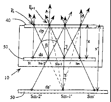
Figure 2 illustrates the method of the illumination of the individual P 1-Pn
pix-
els. As may be seen from Fig 2, there is arranged a second light emitting sur-
face 50 behind the first light emitting surface 40, the latter comprising the
pix-
els P. The second light emitting surface 50 comprises light emitting points S1-
Sm. One light emitting point Sj illuminates several pixels Pk, i. e. produces
light for several pixels Pk. Let us assume that the distance ds between the
light
emitting points S is equal to the distance dp between the pixels P. Watched
SUBSTITUTE SHEET (RULE 26)
CA 02250968 1998-10-02
WO 98/34411 PCT/HU98/00012
-9-
from within a few meters distance, an impression of a spatial (three-
dimensional) image with an acceptable quality may be achieved, if the differ-
ence angle between the light beams emitted into neighbouring directions is not
larger than 1 °, e. g. equal to 1 °. A good resolution for the
purpose of the image
details and contrast may be achieved if the distance dp between the pixels P
is
approx. 1 mm, or smaller. Assuming the simple case that the value of the view
angle is 60°, and the exit angle (3 of the light emitting points Sl-Sm
is also 60°,
then it is obvious that one light emitting point S must illuminate 60 pixels P
to
achieve 1 ° angle resolution. If the distance dp between the pixels P
is 1 mm.
than 60 pixels P cover a 6 cm long line. In this case the distance x between
the
first light emitting surface 40 and the second light emitting surface 50 is ap-
prox. 5,2 cm. But to have 60 different emitting directions for each pixels P,
the
number of the light emitting points S1-Sm must be equal to the number of pix-
els P. In this case the distance ds is also equal to the distance dp, i..e. ds
= 1
mm. This may be an obstacle in realising the light emitting points S1-Sm in
practice.
As it is illustrated in Fig. 2, by increasing the distance x between the first
light
emitting surface 40 and the second light emitting surface 50 - in Fig. 2 this
is
illustrated by increasing x to x' -, the distance ds will increase as well,
provid-
ing substantial advantage to a practical realisation of the light emitting
points
Sl'-Sm'. As it will be shown below, in this case the angle resolution of the
in-
dividual light emitting points S1'-Sm' must increase in return. It is also
clear
from Fig. 2, that by increasing the distance x with a factor of two, e.g. in
this
case to the distance x', the distance ds' between the light emitting points S
will
be also two times the distance dp. At the same time, the angle resolution must
increase, that is practically the angle y between the neighbouring light
emitting
directions of a light emitting point S will decrease. At the same time, as it
is
seen from Fig. 2., that by increasing the distance from x to x', the light
beam
originating from the light emitting point Sm-2 in the direction of the pixel
Pq,
due to the displacement of the second light emitting surface 50 backwards, is
now originating from the light emitting point Sm-1'. At the same time the
light
emitting point Sm-1' must still provide light for the pixel Pq+1. Hence it fol-
lows that by increasing the distance ds, not only must the angle resolution of
the
SUBSTITUTE SHEET (RULE 26)
CA 02250968 1998-10-02
WO 98/34411 PCT/AU98/00012
- 10-
individual light emitting points S increase, but also the number of possible
emitting directions of the light emitting points S. E.g. by increasing the
distance
x five-fold, then the necessary angle resolution, i. e. the smallest value of
y is
0.2°, while the number of served directions is 5 x 60 = 300. In
exchange, the
total width of a light emitting point S may reach as much as 5 mm, which is
sufficient for the realisation of such light emitting points S that are
suitable for
a suggested practical solution.
It must be stressed, that in the following descr iption the arrangement of the
light emitting points will be explained in only one dimension. However, there
is
nothing in the way to realise the arrangement according to the invention along
both co-ordinates, i. e. horizontally and vertically as well, and thus to
provide
display which makes fully realistic spatial imaging possible.
With reference to Fig. 3, there is shown a practical realisation of a light
emit-
ting point S. This comprises a laser L, this being preferably a diode laser,
but it
is understood that other types of lasers, e.g. gas-, solid state or dye lasers
are
also suitable. The light of the laser L is deflected in vertical direction -
along
the Y axis - in a suitable angle by the deflector AOy. The horizontal
deflection
is performed in an analogous manner by the deflector AOx. The deflectors
AOx and AOy are constructed as acousto-optical devices, in a known manner.
But other suitable optical deflector means may be used as well, e. g.
polygonal
mirrors, galvanic mirrors, hologram discs, electro-optical devices (e. g. Kerr-
cells}, variable refraction index LCD devices or the like.
Considering that with known acousto-optical deflectors only relatively small -
approx. 2° - deflection angles may be achieved, , the exit angle ~3 of
the light
emitting points S must be magnified. This magnification is performed by the
angle magnifier D, a possible embodiment of which is shown in Fig. 4. Here
the angle magnifier D is shown as an optical arrangement comprising tradi-
tional collecting and dispersing lenses 52 and 54. Generally, D comprises a
known telescopic lens arrangement, with appropriate apertures. It must be
noted
that the angle magnifier D may be advantageously used for filtering out the
zero
order, non-deflected beam of the deflectors AO, using apertures and dia-
SUBSTITUTE SHEET (RULE 26)
CA 02250968 1998-10-02
WO 98/34411 PCT/HiT98/00012
-11-
phragms (not shown). With a specific embodiment, the light emitted from the
angle magnifier D is magnified approx. fivefold, i. e. the exit angle ~3 is
approx.
10°.
Fig 5. shows that with the arrangement of light emitting points S placed
beside
each other and associated angle magnifiers D light beams from the individual
light emitting points S are arriving from different directions and with
different
intensities to the different pixels P of the first light emitting surface 40.
But the
angle magnification practically attainable by the angle magnifier D is still
not
sufficient to provide the desired view angle. Therefore, a further angle
magnifi-
cation may be necessary in the pixels P, which may be performed in a preferred
embodiment by the micro-lens system 46 as shown in Fig. 7.
Returning to Fig. 6a, the light beams emitted from the pixel P in neighbouring
directions ik and ik+1 have an angle of y. As mentioned, the value of the
angle
y is smaller than 1 °. However, to have the impression of a continuous
image, it
is necessary that the beams emitted in the neighbouring directions ik and ik+1
are at least adjacent. Thus it follows that the divergence 8 of the beams
emitted
from the pixels P must be at least as large, but preferably slightly larger
than the
angle y, i. e. the angle resolution within the view angle oc, of the pixels P.
To
obtain this, an optical element must be provided on the first light emitting
sur-
face 40 to ensure the appropriate divergence 8 of the beams emitted from the
pixels P, this latter divergence 8 in practice being approx. 1 °. This
optical ele-
ment may be constructed as a holographic element 42, which may be an ele-
ment comprising several discrete sub-elements associated with one or more
pixels P, as shown in Fig. 6a, but may also be constructed as a single optical
element covering the whole screen.
If we give up the demand to have spatial imaging along the Y - direction, and
arrange the light emitting points in only one row, as will be discussed more
in
detail below, then the necessary dispersion or divergence along the Y
direction
may be provided by the holographic element 42, as shown in Fig. 6b.
As mentioned above, Figs. 7a and 7b show a possible embodiment for per-
SUBSTITUTE SHEET (RULE 26)
CA 02250968 1998-10-02
WO 98/34411 PCT/HIJ98/00012
- 12-
forming further angle magnification in the plane of the screen. There is pro-
vided on the first light emitting surface 40 a micro-lens system 46, which fur-
ther increases the angle of the incident light beams. The micro-lens system 46
may be manufactured with a known technology, e. g. using optical grade poly-
carbonate or other plastic with similar properties. It is also possible to
make the
micro-lens system 46 of two sheets, and including a further dispersion layer
48
between them. The dispersion layer 48 disperses the light beams in the y-
direction, if spatial imaging is realised only along the x-direction in the
appa-
ratus 10. The dispersion layer 48 may be constructed as a traditional optical
cylindrical lens system or holographic element, or in another known manner.
The dispersion layer 48 may also provide the necessary horizontal (or
vertical)
divergence b of the beams, or this latter may be obtained with further optical
elements. The role of the vertical divergence or dispersion will be discussed
below.
Figs. 8 a-c illustrate the internal structure of the laser- and modulator unit
20.
Within the laser- and modulator unit 20 there is a 22 modulator block, com-
prising the modulator controller 24 and the deflectors AOx and AOy. With the
preferred embodiment shown in Fig. 8a there is one separate deflector AOx
and AOy for each laser L. Each deflector is connected to a common modulator
controller 24. Essentially, it is the modulator controller 24 that controls
the in-
dividual deflectors according to the signal IN containing the three-
dimensional
information, and organises the emitted light intensities as a function of the
ap-
propriate light emitting directions in such a manner, that the desired image
will
appear when viewing the P pixels from the different directions. Fig. 8b shows
a
solution where the lights of all lasers L are deflected and modulated respec-
tively by a larger common deflector AOx and AOy, preferably constructed as a
large acousto-optical single crystal. This solution offers the advantage that
the
construction of the modulator controller is simpler. Its disadvantage is that
it
makes the device slower, because at least as much time must pass between
modulating two lasers, so that there is enough time for the generated ultra-
sound wave to traverse the whole acousto-optical crystal. Using crystals that
are
too large may make the system unacceptably slow. As an intermediate solution
it is also possible to use the system shown in Fig. 8c, where several, not
very
SUBSTITUTE SHEET (RULE 26)
CA 02250968 1998-10-02
WO 98/34411 PCT/HI198/00012
-13-
long crystals are used as deflectors AOx and AOy, but one deflector modulates
the light of several lasers L. As shown, it is also possible to use with more
sepa-
rate x or y direction deflectors AO with one common x or y direction deflector
AO. It is understood that the x or y direction deflectors need not be working
with the same principle. it is straightforward to combine within the modulator
block 22 one or more acousto-optical deflectors with one or more deflectors
based on a polygonal minor, galvanic mirror or other principle.
As shown in Fig. 5, it appears that the pixels P placed on the edge of the
first
light emitting surface 40 can not be reached by the light beams of a
sufficient
number of light emitting points S. This may be overcome by placing light emit-
ting points S also further to the side, beyond the outer pixels P. But this
would
mean that the width of the apparatus 10 would increase in an undesirable man-
ner, and the capacity of these outer light emitting points S would not be used
to
full extent. An improved embodiment of the invention with a suggested solu-
tion to overcome this problem is shown in Figs. 9a-b. Here it is shown that
the
space between the first light emitting surface 40 and the second light
emitting
surface 50 is closed on the two sides by the mirrors M. In this manner those
light beams of the outer light emitting points S, e. g. of the points S l and
S2,
that would otherwise be lost, because they fall in an angle interval that is
not
used. will be reflected from the mirrors M into the pixels P close to the
edge,
e.g. into the pixel P1. As it appears from Fig. 9a, the reflected beams seem
to
arrive from the virtual light emitting points Sl' and S2' into the pixel P1.
In a
practical embodiment such beam trajectories are also possible, where the beams
emitted from the light emitting points S will be reflected not only from one
of
the mirrors M, but from both mirrors M, even undergoing multiple reflections
if
necessary. A few such beams undergoing multiple reflections are shown in Fig.
11 a as well.
Fig. 9b illustrates that the number of the light emitting points S may be much
smaller than the number of the pixels P. In an extreme case only one light
emit-
ting point S is sufficient to illuminate all pixels P. It is conceivable from
the
above, however, that with the increase of the number of pixels P associated
with a single light emitting point S, the number of directions (direction
angles)
SUBSTITUTE SHEET (RULE 26)
CA 02250968 1998-10-02
WO 98/34411 PCT/HiJ98/00012
- 14-
provided by the light emitting point S must increase as well. If the angle
reso-
lution is kept constant, the exit angle ~3 of the light emitting point S must
in-
crease, or with a constant exit angle (3 the angle resolution must be
increased.
Of course, the angle resolution and the exit angle may be increased simultane-
ously as well.
Referring to Figs. l0a-b, another possible embodiment of the light emitting
points in the apparatus IO is presented. In this embodiment, so-called spatial
light modulators (SLM) are utilised as deflectors. These deflectors SLM are
illuminated with a suitable light source, preferably a laser (not shown). The
light beams reflected in different directions from the extending surface of
the
deflectors SLM are imaged on the pixels P with a known optical system, in the
presented embodiment with the focusing means 60. The focusing means 60 is
practically constructed as a projection lens system. Devices applicable as de-
I S Electors SLM are off-the shelf items. Considering that the useful
controllable
surface of these devices is normally smaller, than the physical full width of
the
device, in a given case it may not be possible to arrange sufficient number of
deflectors SLM beside each other in one line. This may be overcome by ar-
ranging the deflectors SLM in two (or more) lines, as shown in Fig. lOb, and
by
guiding the light beams exiting from each line into a common plane with a suit-
able optical system.
Generally, a deflector SLM may be regarded as a small display, providing a
two-dimensional image. However the "image" provided by the individual de-
Electors SLM do not correspond to any real image, but instead it is a sum of
image segments, where the image segments represent different images, i. e. im-
age signals of the different points of the object, these different images
repre-
renting different view angles during the generation of the three-dimensional
image signal. The projected two-dimensional images, i. e. the image segments
are mixed by the system into a unified three-dimensional image, in such a man-
ner, that when viewing the screen from a given angle, the image segments seen
from that view angle will be placed beside each other again.
As mentioned above, the apparatus 10 may be realised using only one single
SUBSTITUTE SHEET (RULE 26)
CA 02250968 1998-10-02
WO 98/34411 PCT/HU98/00012
-15-
light emitting point S, which will provide light beams from a suitable number
of directions for every pixel P, i. e. for n pixels P. Fig. 11 a shows such a
sys-
tem. In accordance with the above, it is conceivable that if light beams have
to
be emitted in k different directions with different intensities from a pixel
P,
than this single light emitting point S must be able to radiate light in k x n
di-
rections. Such angle resolution or exit angle can not be obtained with
deflector
means based on the acousto-optic principle. Therefore, Fig. 11 b shows the
schematic diagram of a light emitting point S, comprising a polygonal mirror
62
performing deflection in the x-direction and a polygonal mirror 64 performing
deflection in the y-direction. The beams reflected from the polygonal mirrors
are imaged and formed to the desired properties with a known optical system
66.
It is straightforward to reduce the amount of data necessary, or the number of
elements used in the system, by combining the arrangement of the invention
with known solutions. A possible solution to give up the spatial effect along
one co-ordinate. This may be done because the perception of a spatial image is
primarily caused by the difference of the images in horizontal directions.
This is
caused by the fact that the plane defined by our right and left eye is
normally
horizontal, and therefor we only see the objects differently in horizontal
direc-
tion. This means that the vertical parallax may be omitted, and thus the
amount
of transferred information may be substantially reduced. Once more it must be
emphasised that with the invention it is possible to create a spatial image
both
in vertical and horizontal directions.
The amount of information transferred and processed may be further reduced
by reducing view angle and the number of directions distinguished within the
view angle to a practically treatable and realisable value. It has been found
that
using a view angle of 30-40° and choosing the angle differences between
the
viewing directions to 1-2°, spatial (three-dimensional) images with an
accept-
able quality may be created.
If the 3D-effect along the Y-axis is omitted, it is sufficient to use one row
of the
light emitting points S. Since the vertical dimension if the light emitting
points
SUBSTITUTE SHEET (RULE 26j
CA 02250968 1998-10-02
WO 98/34411 PCT/HU98/00012
- 16-
S is no longer critical, these may be realised as relatively narrow, but tall
optical
modules, which may be placed close to each other, and therewith creating a row
of light emitting points S. A specific, preferred embodiment of such an
optical
module O is shown of Fig. 12. The optical module O is housed in a flat, long
metal block, and the optical and electronic elements are positioned more or
less
in one plane, to make the optical module O as narrow as possible, and
therewith
enabling to place a relatively large number of modules beside each other. With
the shown preferred embodiment, 60 modules are used, approx. 1 cm apart. The
optical modules O all has an identical structure. The optical module O com-
prises the light source L and the deflectors AOy and AOx, and the angle magni-
fying optics. The light source L is a diode laser, while the deflectors AOy
and
AOx are acousto-optical devices. The laser diode and the deflectors AOy and
AOx are controlled by the driving circuit DRC. The light beam emitting the
deflector AOy goes through the angle magnifier, which contains the telescopic
lens system T and one or more apertures A. The angle magnifier also includes
cylindrical lenses, to correct the asymmetrical deflecting properties of the
acousto-optical modulator devices. The apertures in the telescopic lens system
T filter out the non-modulated zero order beam of the acousto-optical deflec-
tors, and improve the resolution of the telescopic lens system T. At the upper
end of the module O, the emitted light beam is deflected towards the first
light
emitting surface, i. e. the screen by the deflecting mirror DM. The optical
mod-
ule O is connected electronically to a mainboard MB carrying the control elec-
tronics CE via connectors C, the latter positioned at the bottom of the
optical
modules OI...Om. The body of the optical modules Ol...Om are preferably
made of a rigid metal, like high-grade aluminium, in order to provide a solid
base for the optical elements, but with good thermal dissipation, because the
acousto-optical modulators need efficient cooling.
Omitting the vertical parallax it is advantageous to position such optical ele-
ments in the pixels, which in the horizontal direction appropriately deflect
the
incident light beams or transmits them unchanged, but in vertical direction
dis-
perses the light in a vertical plane containing the travelling direction of
the light
beam. The result is that the emitted light beams become visible, practically
in-
dependent of the height of the eyes of the person watching the screen, and the
SUBSTITUTE SHEET (RULE 26)
CA 02250968 1998-10-02
WO 98/34411 PCT/HiJ98/00012
- 17-
visible range of the image will not be confined to a narrow horizontal strip.
A
dispersion with this characteristics may be produced with holographic optical
elements or cylindrical optical elements having a horizontal axis. A known so-
lution to this problem is disclosed in W094/23541.
In connection with the vertical dispersion of the light beams emitted from the
screen, there is also another problem, which has to be corrected. As shown in
Fig. 13, the dispersion of the light beams entering the screen and radiated in
the
viewing field is not homogenous. Firstly, the central beam is always stronger,
than the light beams dispersed to the sides. Secondly, this brighter central
beam
will be pointing in different directions, depending from the position of the
pixel
on the screen. Hence, the viewers will be able to perceive and locate the row
of
the light emitting points (i. e. the exit pupils of the telescopic lenses,
reflected
in the deflecting mirrors M) as a relatively bright line behind the screen. To
correct this disturbing phenomenon, further angle correcting elements are
needed on the screen. The function of these angle correcting elements is to
make the vertically deflected light beams of the optical modules O enter the
dispersing means on the screen (first light emitting surface 40) from parallel
directions.
To achieve this effect, several embodiments are foreseen. A few of these are
depicted schematically in Figs. 14a-c.
With the embodiment in Fig. 14a, the vertical dispersion is achieved by a holo-
graphic screen, where the hologram H 1 is applied directly on the surface of
the
first light emitting surface 40. The transformation of the diverging vertical
beams into parallel beams is made by a horizontally oriented cylindrical
Fresnel
lens screen FL. This latter is placed behind the first light emitting surface
40.
Another possible embodiment, depicted in Fig. 14b includes a combined holo-
graphic and Fresnel lens screen. In this case the two sides of the same first
light
emitting surface 40, i. e. the screen of the apparatus are provided with the
holo-
graphic surface structure H2 on the outside (looking towards the viewer), and
a
horizontally oriented cylindrical Fresnel lens surface FLS on the inside
(looking
towards the optical modules). The stl-uctured surfaces may be manufactured
using known methods, like embossing, moulding or etching.
A third embodiment, comprising a combined holographic screen H3 is shown
SUBSTITUTE SHEET (RULE 26)
CA 02250968 1998-10-02
WO 98/34411 PCT/AU98/00012
- 18-
in Fig. 14c. In this latter case, the combined holographic screen H3 performs
both the vertical dispersion of the light beams and the necessary divergent-to-
parallel beam correction.
Fig. 15 illustrates the spatial arrangement of the elements of the optical
system
in a preferred embodiment of the 3D-display apparatus according to the inven-
tion. The optical modules O1-Om serving as the light emitting points are ar-
ranged in a row at the backside of the apparatus, stacked parallel and closely
to
each other, with the exit aperture of the telescopic lens system T looking up-
wards, so that the deflecting mirrors DM will project the light beams towards
the screen positioned on the front side of the apparatus. Two triangularly
shaped minors M close the two sides of the projection space. The control elec-
tronics CE, and the power supply PS are located under the optical system. The
power supply PS powers the control electronics CE, the light sources L and the
acousto-optical modulators AOx and AOy in the optical modules O1-Om. The
optical modules O1-Om are placed on a common mainboard MB of the control
electronics (not shown in Fig. 15), and connected thereto electronically with
the
connectors C. The physical configuration of the optical modules O with the
mainboard MB of the control circuit and the connectors C is shown in Fig. 16.
The colour version of the display apparatus may be provided using known so
lutions. A possible method is to make the light emitting points S with the
three
basic colours - red, blue, green - and mixing the differently coloured light
beams using known optical methods, either before or after the deflectors AO or
after the angle magnifiers D.
SUBSTITUTE SHEET (RULE 26)