Note: Descriptions are shown in the official language in which they were submitted.
CA 022~1474 1998-10-26
TT~'RMTN8T- CONNECTOR CAPABLE OF ATTA'-Hr-~:~L
TO A METALLIC SURFACE
BACKGROUND OF THE INVENTION
1. Field of the Invention
The present invention relates generally to terminal
connectors. More particularly, the present invention
relates to a terminal connector attachable to a metallic
surface by friction joining.
2. Disclosure Information
Practically all automotive vehicles produced today
have front and rear glass windshields. It is common
practice to provide one or both of such windshields with a
wire circuit either attached to or embedded within the
windshield. These wire circuits may be used for a variety
of purposes, such as an antennae for sending/receiving
radio frequency signals, a high resistance windshield
defroster circuit, and so forth, as illustrated in FIG. 1.
Here, the windshield 80 has a wire circuit 82 attached
thereto, with each end of the circuit having a termination
84. Typically, each termination 84 has a metal clip-like
connector 86 attached thereto, with a mating external
circuit connector 88 being attached to the clip connector
86. The external circuit 90 in turn may be connected to a
radio, a theft prevention/detection system, a keyless entry
system, a cellular phone, a power circuit for defrosting
the windshield, etc.
The typical method used to attach the metal connector
86 to the glass windshield 80 involves the following steps.
First, a glass particle/silver particle paste or "frit" is
CA 022~1474 1998-10-26
deposited onto the windshield adjacent to and in contact
with the circuit termination 84. Second, the fritted
windshield is fired in an oven such that the glass of the
windshield and the glass particles in the frit soften so as
to bond to each other. This causes the fired frit deposit
-- at this point referred to as a "pad" -- to bond to the
glass, while the silver particles distributed throughout
the pad create an electrically conductive path from the
termination 84 to the top surface of the pad. Third, a
predetermined amount of solder is deposited atop the pad.
And fourth, the metal clip connector 86 is placed on the
solder and the solder is heated to a temperature well above
its melting point and then allowed to cool, so that the
clip is soldered to the pad.
However, this approach presents a problem in that the
heat used to melt the solder also increases the risk of
cracking the adjacent windshield glass. Furthermore, upon
cooling from these elevated temperatures, there is a
tendency for one or more of the connector, solder, pad, and
glass to delaminate and/or debond from each other due to
the large differences among their respective coefficients
of thermal expansion.
It would be desirable, therefore, to provide a
terminal connector and a method for attaching the same to a
windshield or other fragile workpiece without subjecting
the workpiece to the elevated temperatures presented by
previously known processes.
SUMMARY OF THE INVENTION
The present invention overcomes the disadvantages of
the prior art by providing a terminal and a method for
attaching the same to a metallic surface on a workpiece
using friction joining. One embodiment of the terminal
. CA 022~1474 1998-10-26
comprises an electrically conductive body 22 having a top
end 24 to which an electrical connector 70 may be attached,
a bottom end 26 having a bottom surface 28 generally
conforming to the mating surface 52 of the workpiece 50,
and an axis R substantially orthogonal to the bottom
surface 28 about which the terminal 20 may be rotated.
Attached to the bottom surface 28 is a layer of solder 30
having an outer perimeter 32 and defining a central solder-
free region 34 about the axis R. In a preferred
embodiment, the bottom surface 28 of the terminal 20 is
substantially circular in shape, and the layer of solder 30
is substantially annular in shape with the central solder-
free region 34 being substantially circular and generally
centered about the rotational axis R. The solder layer 30
may further define a plurality of evenly spaced radial
grooves 38 therein.
It is an object and advantage of the present invention
that attachment of the terminal to the workpiece as
described herein exposes the workpiece to significantly
less heat than is the case with conventional methods, such
as soldering. This reduces the risk of damaging the
workpiece.
These and other advantages, features and objects of
the invention will become apparent from the drawings,
detailed description and claims which follow.
BRIEF DESCRIPTION OF THE DRAWINGS
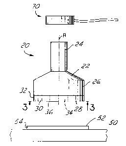
FIG. 1 is a perspective view of a clip terminal
attached to a glass windshield of an automotive vehicle
according to the prior art.
3s FIG. 2 is an elevation view of a terminal according to
a first embodiment of the present invention.
-- 3 --
CA 022~1474 1998-10-26
FIG. 3 is an end view of the terminal shown in FIG. 2
as viewed along line 3-3.
FIG. 4 is an elevation view of a terminal according to
an alternative first embodiment of the present invention.
FIG. 5 is a section view of the terminal shown in FIG.
4 as viewed along line 5-5.
FIGS. 6-8 are bottom views of a terminal according to
a first embodiment of the present invention.
FIG. 9 is an elevation view of a terminal according to
a second embodiment of the present invention.
FIGS. 10-11 are bottom views of a terminal according
to a second embodiment of the present invention.
FIGS. 12-13 are section views of a terminal according
to a second embodiment of the present invention.
DETAILED DESCRIPTION OF THE PREFERRED EMBODIMENTS
Referring now to the drawings, FIG. 2 shows a terminal
connector 20 attachable to a metallic mating surface 52 on
a workpiece 50 by friction joining according to a first
embodiment of the present invention. The connector 20
comprises an electrically conductive body 22 having a top
end 24 to which an electrical connector 70 may be attached,
a bottom end 26 having a bottom surface 28 generally
conforming to the mating surface 52 of the workpiece 50,
and an axis R substantially orthogonal to the bottom
surface 28 about which the terminal 20 may be rotated.
Attached to the bottom surface 28 is a layer of solder 30
having an outer perimeter 32 and defining a central solder-
free region 34 about the axis R.
CA 022~1474 1998-10-26
In a preferred embodiment, the body 22 is
substantially rigid and is constructed of aluminum and/or
copper. The bottom surface 28 of the terminal 20 is
substantially flat and substantially circular in shape, and
the layer of solder 30 is substantially annular in shape
with the central solder-free region 34 being substantially
circular and generally concentric with the rotational axis
R, as shown in FIGS. 2 and 3. The terminal 20 may be
symmetric about its rotational axis R (i.e., the terminal
shape may be a solid of revolution) as shown in FIG. 2, or
it may assume some other shape, such as the configuration
illustrated in FIG. 4. The solder-free region 34 may extend
from the solder layer mating surface 36 completely down to
the bottom surface 28 of the body 22 as shown in FIG. 2, or
it may extend down to only a portion of this depth, as
illustrated in FIGS. 4 and 5. Of course, other
configurations of bottom surface 28, solder layer 30, and
central solder-free region 34 are possible which are still
within the scope of the present invention.
The terminal 20 may be attached to the workpiece 50 in
the following manner. First, the workpiece 50 is held
stationary while the terminal 20 is rotated about its
rotational axis R. The specific rotational speed used will
depend on several factors, such as the surface area of the
solder layer 36, the size of the solder-free region 34, the
solder composition used, the thermal and mechanical
characteristics of the workpiece mating surface 52 to which
the solder layer 30 is to be attached, etc. Generally,
though, the speed will be in the range of lO00 to 8000 RPM,
with 4000 RPM being nominal. Second, the mating solder
layer surface 36 of the rotating terminal 20 is brought
into contact with the mating surface 52 of the workpiece 50
for a predetermined length of time and using a
predetermined amount of "forging" force. The same factors
affecting rotational speed will likewise affect the
. CA 022~1474 1998-10-26
specific length of time and amount of force used. For
example, experiments using copper terminals with a 0.357-
inch to 0.418-inch diameter bottom surface with a
conventional tin/lead solder layer of the same diameter
having a 0.125-inch diameter central solder-free region
produced satisfactory results using 120 pounds of force
(i.e., 220 to 300 p.s.i.) with 1 to 6 seconds of rotational
contact. Third, the rotation of the terminal 20 is
abruptly stopped, preferably within a single revolution and
most preferably within one-tenth of a revolution.
When the rotating terminal and stationary workpiece
are forced together for a short time, followed by an abrupt
stoppage of the rotation, a bond is formed between the
terminal and workpiece. Scanning electron micrograph (SEM)
samples show that a galling action occurs between the
solder in the solder layer and the metal in the workpiece
at the interface between the mating surfaces 36/52, thereby
forming the bond. The samples also show that during the
rotational contact, some of the solder becomes plastically
deformed -- but not quite melted -- due to the heating and
shearing caused by the rotational contact, and is smeared
between the mating surfaces. These samples further
indicate that a strong bond can be formed (1) without
generalized melting of the solder and (2) without the
appreciable formation of intermetallic compounds. This is
in contrast with conventional soldering, which normally
requires both melting of the solder and the formation of
intermetallics. Of course, increasing the rotational
speed, forging force, and/or rotational contact time will
in fact cause a more generalized melting of the solder and
formation of intermetallics to occur, with a resultant
strong bond; however, it is important to note that the
additional speed, force, and/or time are not necessary in
order to form an acceptably strong bond between the
terminal and workpiece.
CA 022~1474 1998-10-26
An important aspect of the present invention is the
central solder-free region 34. The importance of this
region 34 can perhaps best be illustrated by explaining how
its absence would affect the above process. If the solder
S layer 30 had no central solder-free region -- e.g., if it
were disk-shaped rather than annular -- the tangential
component of the rotational speed of the solder located in
the center of the layer (i.e., adjacent the axis R) would
approach zero. With such little tangential speed, very
little friction and heat are developed there, thus
preventing the solder in this region from plastically
deforming. Although solder proximate the outer perimeter
32 would tend to plastically deform due to the much higher
tangential speed there, once the thin layer of plastically
deformed solder smears away, the non-plastically-deformed
region at the center would prevent further solder near the
perimeter from becoming sufficiently plastically deformed.
With the central region remaining relatively solid, that
plastically deformed portion of the solder near the
perimeter would tend to be spun outward beyond the
perimeter where it would no longer experience the forging
pressure between the mating surfacesi here the spun-out
solder would cool and form solder flash.
However, in the present invention there is no solder
in the central region, thus alleviating the above problem.
Also, the central solder-free region provides a reservoir
where plastically deformed solder can be pushed into as the
terminal and workpiece are in rotational contact with each
other.
This embodiment can be further improved by providing
one or more additional solder-free regions 38 in the solder
layer 30 between the central solder-free region 34 and the
3s outer perimeter 32. Each additional region 38 may be
contiguous with the central solder-free region 34 and/or
.
' CA 022~1474 1998-10-26
.
with the outer perimeter 32 of the solder layer 30, or may
be non-contiguous with both. The shape of each region 38
may be circular, square, ellipsoidal, or any other shape,
as illustrated in FIG. 6, with the preferred shape being
that of a radial groove contiguous with both the central
region 34 and the outer perimeter 32, as illustrated in
FIG. 7. When more than one additional region 38 is
provided, they should preferably be substantially evenly
spaced about the rotational axis R.
It should be noted that the terminal 20 can also have
radial grooves 38 as illustrated in FIG. 8. Here, the
radial grooves can be viewed as "diametrical" grooves which
"cross" in the center of the solder layer and define a
IS central solder-free region 34 thereat. Thus, it is
possible to have one or more radial grooves which
inherently define a solder-free central region at the
center from which they radiate, without there necessarily
being a separately defined central solder-free region.
As the terminal 20 is rotated in contact with the
workpiece 50, plastically deformed solder can be smeared
away into the additional region(s) 38, thereby exposing
more solder underneath the smeared away solder as the
terminal 20 continues to rotate. It is preferable that
succeeding layers of not-yet-plastically-deformed solder be
exposed because solid (i.e., not-yet-plastically-deformed)
solder provides much higher friction with the mating
workpiece surface 52 than does plastically deformed solder.
This higher friction helps heat the mating surfaces 36/52
much quicker so that enough heat is generated to facilitate
the galling bond upon stoppage of the rotational motion
without transferring as much heat to the workpiece (which
may be important if the workpiece is heat-sensitive).
- CA 022~1474 1998-10-26
As an alternative to using rotational motion to effect
a bond between the terminal and the workpiece, reciprocal
motion may be used instead, in conjunction with a second
embodiment of the present invention. A ~reciprocal"
terminal 120 suited for this type of motion, as illustrated
in FIG. 9, would differ from the ~rotational~' terminal 20
of the first embodiment described above in at least two
respects. First, there would be no concern whether the
reciprocal terminal 120 has a rotational axis R (although
it geometrically may have a rotational axis and yet be
otherwise adapted for reciprocal motion). And second,
there would be no need for a central, solder-free region
(although it could have one). Like the rotational terminal
20, a reciprocal terminal 120 would comprise an
electrically conductive body 122 having a top end 124 to
which an electrical connector 170 may be attached, a bottom
end 126 having a substantially flat bottom surface 128,and
a layer of solder 130 attached to the bottom surface 128.
In the present embodiment 120, the solder layer 130 defines
at least one solder-free region 138 thereini each region
138 may be circular (as illustrated in FIG. 10), square,
ellipsoidal, diamond-shaped, or any other geometric shape.
In a preferred embodiment, the solder layer 130 defines a
plurality of substantially straight longitudinal solder-
free grooves 138 oriented substantially parallel with adirection D in which the terminal 120 may be reciprocated,
as illustrated in FIG. 11. These grooves may extend across
the entire solder layer surface 136 and be contiguous with
the outer perimeter 132 at either end, as in FIG. 11, or
they may be contiguous therewith at only one or neither
end.
The grooves may assume a profile such as shown in
FIGS. 12 and 13, or they may assume other profiles. As
with the rotational terminal 20, the depth of the solder-
free region(s) 138 may extend from the solder layer mating
CA 022~1474 1998-10-26
surface 136 completely down to the bottom surface 128 of
the body 122 as shown in FIG. 12, or may extend down to
only a portion of this depth, as illustrated in FIG. 13.
S The reciprocal terminal 120 may be attached to the
workpiece 150 in either of the two following approaches.
In the first approach, the terminal 120 and the workpiece
150 are brought into contact with each other such that
their respective mating surfaces 136/152 contact one
another. Next, either the workpiece or the terminal is
held stationary, while the other is reciprocated rapidly
back-and-forth across the mating surface interface at a
predetermined rate while a predetermined forging force is
applied substantially orthogonal to the mating surface
Is interface so as to press the terminal and workpiece
together. The reciprocating motion and forging force are
maintained for a predetermined length of time, in order to
heat the solder and workpiece surfaces 136/152 enough to
promote galling of one metal into another without
necessarily requiring (but not necessarily precluding)
melting of the solder. Then, the reciprocating motion is
abruptly stopped, preferably within a single stroke, while
the forging force is maintained. This creates a bond
between the terminal and workpiece mating surfaces 136/152,
similar to that created in the first embodiment above. The
forging force may then be relieved and the bonded
terminal/workpiece combination used in any subsequent
process, such as in the attachment of an electrical
connector 170 to the top end 124 of the terminal 120.
Alternatively, a second approach to bonding together
the terminal and workpiece involves switching a couple of
steps from the first approach. Namely, either the
workpiece or terminal is held stationary and the other is
reciprocated rapidly back-and-forth at a predetermined
rate, and then the workpiece and terminal are brought
-- 10 --
CA 022~1474 1998-10-26
together such that their respective mating surfaces 136/152
are in contact with each other, whereupon a predetermined
forging force is applied substantially orthogonal to the
mating surface interface so as to press the terminal and
workpiece together. In this approach, the reciprocated
member is first brought up to full reciprocating speed
before pressing the terminal and workpiece together. The
remaining steps of the present approach are similar to the
remaining steps of the first approach.
As with the first embodiment, the predetermined force,
rate, contact time, and so forth are determined by such
factors as the size and shape of the respective mating
surfaces, the types of metals comprising the solder and
workpiece mating surfaces, the specific configuration of
solder-free regions used, any process constraints which
must be accommodated, etc.
In the present embodiment, the solder-free regions 138
(e.g., the longitudinal grooves) provide reservoirs where
the plastically deformed solder may be smeared into so that
solder beneath the smeared away plastically deformed solder
can come into contact with the workpiece surface 152 and
generate increasing friction and heat. This continuous,
rapid process of heating up the surface layer of solder,
plastically deforming it, smearing it away into the solder-
free regions, exposing new layers of solder, and repeating
the cycle, quickly brings the workpiece surface and the
interfacing solder layer up to a temperature sufficient to
facilitate interfacial galling of one metal into the other,
without necessarily requiring (but not necessarily
precluding) a generalized melting of the solder.
Various other modifications to the present invention
will, no doubt, occur to those skilled in the art to which
the present invention pertains. For example, the workpiece
CA 022~1474 1998-10-26
mating surface 52/152 may be any portion of the workpiece
surface if the workpiece is made of metal or at least has a
metallic surface; alternatively, the mating surface 52/152
may be a metallic or metallized member attached to the
workpiece. An example of this latter arrangement would be
a glass windshield workpiece having a metallic pad adhered
or fritted to the windshield; here, the metallic pad would
be the workpiece mating surface 52/152. Also, the terminal
can be entirely made of metal (e.g., aluminum, copper,
etc.), or it can be made of plastic, ceramic, and/or other
materials with a full or partial coating or piece of metal
attached thereon or therein, or it can be made of a
conductive ceramic or polymer; any of these configurations
would provide the necessary electrically conductive path
S between the top end 24/124 and the bottom surface 28/128.
Additionally, the bottom surface 28/128 of the terminal
20/120 may be somewhat curved to accommodate any curvature
of the workpiece mating surface 52/152. Furthermore, as
used herein, "plastically deformed" solder can encompass
melted solder, whether the melting is localized or
generalized, but doesn't necessarily require that the
solder be melted. As noted above, it is not necessary to
the present invention that the solder layer 30/130
generally or locally melts, but such melting is not
precluded by the approach of the present invention. It is
the following claims, including all equivalents, which
define the scope of the invention.