Note: Descriptions are shown in the official language in which they were submitted.
CA 022~1967 1998-10-19
W O 98/39812 PCT/AU98/00141
"A high frequency multi-port switching circuit"
Technical Field
This invention concerns a multi-port switching circuit. The
embodiments of one realisation may operate at fiequencies around 60 GHz;
5 but with appropriate devices embodiments may operate at other frequencies
including higher frequencies up to and even exceeding 100 GHz.
Background Art
Switching networks have been developed which operate at frequencies
0 up to and exceeding 40 GHz. The switching elements in such networks use a
combination of shunt passive FET devices and quarter-wave transformers, or
combinations of series and shunt passive FET devices. Passive FET devices,
in one type of switch, require bias to be applied to the gate and not between
the source and drain. Broadband switches using a combination of active and
5 passive switching elements have also been demonstrated.
Snmm~ry of the Invention
The invention provides a multi-port switching circuit, comprising at
least three ports, interconnected by transmission lines. The transmission
20 lines are arranged with a central ring and outwardly extending arms. The
ports are positioned at the ends of respective arms. The term "ring" has been
used in a loose descriptive sense and does not necessarily imply circularity.
A switching device, such as a FET or HEMT, is associated with each
port. The switching device is arranged between a first and a second
25 transmission line. Each switching device may be arranged to shunt the main
signal path of the circuit with its main current path extending between the
junction of the first and the second transmission line, and signal ground.
The first transmission line extends between the port and the switching
device to provide impedance matching, and the second transmission line also
30 provides impedance matching and a connecting path to the ring. The first
and second transmission lines are initially chosen to have lengths of a
quarter wavelength at the centre of the band of operation of the switch. The
dimensions of the matching lines and the lines which form the connections
to the ring are then determined using a procedure to optimise the
35 performance of the circuit.
CA 022~1967 1998-10-19
wo 98/39812 PCT/AU98/00141
The optimisation procedure involves the selection of two of the ports
as the input and output ports of the switching network. The switching
devices associated with these ports are modelled by ON state representations.
The other port, or ports, are isolated, and their associated switching devices
are modelled in the OFF state. Optimisation of the transmission lines
lengths and widths then aims to provide desired performance levels such as
low transmission loss, good isolation at all other ports, low return loss or
high power handling.
Other parameters such as gate width and length and substrate
10 thickness may also be optimised, but these parameters are usually pre-
determined by selection of a particular fabrication process for the switching
circuit.
The optimisation procedure continues by varying the signal t~ow in the
circuit. That is, in the first step, the signals flow from a first port to a second
5 port, with the other ports isolated; in the second step, signals flow from thesecond port to a third port with the other ports isolated. This process
continues until a set of optimised parameters is established for each signal
path configuration. The range of optimised parameters are then examined
and a single best set of parameters is used to complete the design. The
20 optimisation process uses conventional techniques and is able to take into
account the effects of all the bends and discontinuities in the switch.
The optimisation provides similar switching performance between any
pair of ports, independent of the chosen input and output.
The switching devices may be arranged symmetrically around the ring
25 to simplify the optimisation process. However, symmetry is not a
requirement.
HEMTs (High Electron Mobility Transistors) may be used to provide
operation at high microwave frequencies. The choice of switching device
influences, amongst other things, the power-hRnrlling capability of the
30 circuit. Any switching device may be chosen. Two terminal devices, such as
diodes including PIN-diodes; three terminal devices such as generic field
effect devices, for example the FET, MOSFET, MESFET and HEMT; and
multi-terminal devices, such as dual gate devices, could all be used.
Switching devices, such as HEMTs, may be modelled in their OFF
35 state by a resistor and a capacitor in series, and in the ON state by a resistor
CA 022~1967 1998-lo-19
W O 98/39812 PCT/AU98100141
and an inductor arranged in series. However, different and more complex
models can be chosen.
Switching action may be achieved by biasing a pair of HEMTs in their
ON state to create the signal path, while biasing all other HEMTs in their
OFF state. Bias is applied to the gate terminals of the HEMTs, the drain
terminal is connected to the junction between the first and second
transmission lines, and the source terminal is grounded. The OFF or low
impedance state is achieved by applying a DC voltage of zero volts to the gate
terminal. The ON or high impedance state is achieved by applying a DC
0 voltage slightly greater than that required to pinch the device off.
A feature of this circuit is that only a single switching device is
required at each port as a result of optimising the performance of the network
for low losses and high isolation. Thus the switching circuit offers the
benefit of providing a multi-port interconnection requiring an equal number
of switching devices equal to the number of switched ports.
Embodiments of the multi-port switching circuit using HEMTs may
operate in a frequency band around 60 GHz, and are able to provide all the
usual switching functions, such as multiplexing at millim~tre-wave (mm-
wave) frequencies.
Switching networks embodying the invention may be used in multi-
function circuits to allow functionality to be re-configured by altering the
control voltages on the switching devices to re-route the signal.
A circuit cont~ining an embodiment of t-he switching network may
provide the ability to amplify a signal, up-conversion, down-conversion, or
up and down conversion with amplification.
Circuits embodying the invention may offer redundancy that enables
continued operation after failure of a circuit connected to the switching
circuit. For instance, if a switching circuit was arranged to interconnect a
number of identical circuits such as transmit channels, or receive ch~nnels,
failure in any particular channel can be overcome by altering the control
voltages on the switching circuit to re-route the signal path.
When the switching circuit is used to interconnect non-identical
circuits, such as many transmit and receive circuits having different
performance characteristics, then the switching circuit can be configured to
use the transmit and receive circuits which have the most appropriate
characteristics for the current conditions. For instance, if the transmit and
CA 022~1967 1998-10-19
W O 98~9812 PCT/AU98/00141
receive circuits have performance characteristics which make them suitable
for operation in different conditions then the switching circuit may be
configured to use the transmit and receive circuits that are appropriate for
the current conditions, and can be re-configured as conditions change.
Multiple cascades of individual networks can be connected together to
create complicated routing networks. The robustness of the multiple port
configuration allows for redundancy in the design of interconnections
between systems.
0 Brief Description of the Drawings
An example of the invention will now be described with reference to
the accompanying drawings, in which:
figure 1 is a layout of a three port switch embodying the invention;
figure 2 is a graph showing the simulated signal response of the
switching network of figure 1;
figure 3 is a layout of a six port switch embodying the invention;
figure 4 is a graph showing the simulated response of the switching
network of figure 3; and
figure 5(a) is an OFF state model of a HEMT that may be incorporated
into a switch embodying the invention, and figure 5(b) is an ON state model
corresponding to figure 5(a).
Best Modes for Carryinx out the Invention
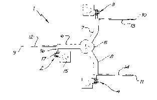
Referring to figure 1, three port switch 1 comprises three transistors 2,
3 and 4 each connected to a central ring 5 by means of respective
transmission lines 6, 7 and 8. The transistors 2, 3 and 4 are each associated
with a respective external port 9, 10 and 11 by means of respective
transmission lines 12, 13 and 14.
Transistor 2 has its source 15 at signal ground, its drain 16 connected
to the transmission lines, and a gate 17. The terminals of transistors 3 and 4
have not been numbered, for the sake of brevity.
In normal operation two of the switches are turned ON to select the
input and output ports.
Figure 2 shows the simulated magnitude responses when the switch is
configured with input applied at port 9 and output taken from port 10; the
magnitude responses for any two sets of ports is nominally identical.
CA 022~l967 l998-lO-l9
W O 98139B12 PCT/AU98/00141
Curve 18 shows the simulated loss from the input port 9 to the output
port 10 to be less than 2 dB at the center frequency of 61 GHz, and to remain
less than 3 dB between 54 to 66 GHz. Curve 19 which shows the input match
to be better than 20 dB at the centre frequency and remains good over a wide
bandwidth; that is greater than 10 dB over 8 GHz of bandwidth. Curve 20
shows the isolation between the input port 9 and the isolated OFF port 11 to
be better than 16 dB.
Referring to figure 3,six port switch 30 comprises six HEMTs 31,32,
33,34,35 and 36 arranged around a central ring 37. Each of the transistors is
connected to the ring 37 by respective lengths of transmission line 38,39,40,
41,42 and 43. The external connection ports 44,45,46,47,48, and 49 are
connected to respective HEMTs by transmission lines 50,51,52,53,54 and
55. The transmission lines provide impedance matching, for both the signal
transmission path and the isolated ports.
Figure 4 shows the simulated magnitude response when the switch is
configured with input applied at port 44 and output from port 47; the
magnitude responses for any two sets of ports is nominally identical.
Curve 56 shows the simulated loss from the input port 44 to the output
port 47is just over 3 dB at the center frequency of 61 GHz, and r~m~in.~ less
than 4 dB between 57 to 66 GHz. Curve 57 shows the input match is better
than 15 dB and remains good over a wide bandwidth; that is greater than 10
dB over 8 GHz of bandwidth. Curve 58 shows the isolation between the
input port 44 and any of the OFF ports is better than 16 dB.
Figure 5 shows the bi-state model of the two finger, fifty micrometer
(ie, 2 by 2511m fingers) wide HEMT used in this embodiment. In the OFF
state shown in figure 5(a) the HEM'r is biased at zero volts. In this state the
HEMT is represented by a 3.2 ohm resistor and a 0.03 picoFarad capacitor
arranged in series. In the ON state shown in figure 5(b), the HEM~ is biased
slightly beyond pinch-off. In this state the HEMT is represented by a 23.4
ohm resistor and a 3 nanoHenry inductance arranged in series.
The switch is optimised using the bi-state model for a stated set of
performance parameters in order to produce the required performance. Any
of the parameters can, of course, be traded against other parameters to
achieve different levels of performance that may be required by different
applications; for instance input match could be traded against power
handling capability. If the circuit were connected to a number of different
CA 022~1967 1998-10-19
WO 98/39812 PCTIAU98/00141
circuits having different performance characteristics then it could be
optimised accordingly.
Although the invention has been described with reference to a
particular embodiment, it should be appreciated that the invention could be
5 embodied in many other forms. For instance, there is no limit on the number
of ports which can form the switching network, symmetry is not a
requirement for the operation of the network, and operation is not limited to
particular process technologies or geometlies for the active devices. Besides
GaAs fabrication technology the invention is applicable to Si and InP
0 processes, among others.
Although this invention has been described with reference to a
switching circuit which operates at about 61 GHz and it is believed to be
useful at much higher frequencies~ it should also be understood that the
invention may be useful in lower frequency switches.
It will be appreciated by persons skilled in the art that numerous
variations and/or modifications may be made to the invention as shown in
the specific embodiments without departing from the spirit or scope of the
invention as broadly described. The present embodiments are, therefore, to
be considered in all respects as illustrative and not restrictive.
. .