Note: Descriptions are shown in the official language in which they were submitted.
CA 022~2102 1998-10-16
DESCRIPTION
TWO-STAGED PROJECTING BUMP OF SEMICONDUCTOR
ELEMENT AND METHOD FOR FORMING THE SAME
TECHNICAL FIELD
The present invention relates to a two-staged
projecting bump of a semiconductor element and a method for
forming the same by bonding a metallic ball formed at a
leading end of a metallic wire to an electrode of the
semiconductor element.
BACKGROUND ART
A conventional two-staged projecting bump and its
formation method will be described with reference to Figs.
12A-20.
Figs. 12A-12F represent a conventional example of
a method for forming a two-staged projecting bump.
In the conventional example, as shown in Fig. 12A,
a metallic wire 1 of gold, copper, aluminum or solder is
passed through a ceramic or ruby capillary 3. A
discharging is brought about between a leading end of the
passed metallic wire 1 and an electrode 6, namely, torch,
whereby a metallic ball 2 is formed at the leading end of
the metallic wire 1.
In Fig. 12B, the metallic ball 2 is pressed onto
a preheated electrode 4 of a semiconductor element 8, to
which an ultrasonic vibration is impressed. The metallic
, .
CA 022~2102 1998-10-16
ball 2 is bonded to the electrode 4 because of the action
of a temperature, a pressure and the ultrasonic vibration.
A reference numeral 5 is a passivation film for protecting
an active face of the semiconductor element 8.
In Fig. 12C, the capillary 3 is raised in a
vertical direction. Then, the capillary 3 is shifted
sideways and descended as in Fig. 12D to bring the metallic
wire 1 into touch with on the metallic ball 2. The
metallic wire 1 is bonded to the metallic ball 2 through
the action of the temperature and pressure or, temperature,
pressure and ultrasonic vibration. The capillary 3 is
moved upward as shown in Fig. 12E, and the metallic wire 1
is pulled and broken as in Fig. 12F, whereby a two-staged
projecting bump 7 is formed.
According to the above-described prior art, when
the metallic ball 2 is formed to the metallic wire 1
through the discharging, crystal grains of the metallic
wire 1 at a part B immediately above the metallic ball 2
(which is denoted as a recrystallized area) are influenced
by the heat and become coarse, as shown in Fig. 13. A
breaking load of the part B is consequently reduced to
nearly half in comparison with a part A not influenced by
the heat.
In a case where the two-staged projecting bump 7
is formed through the processes of Figs. 12A-12F, if a
length of the part B which is decreased in breaking load to
nearly half due to the influences of the heat as described
above is èlongated as shown in Fig. 14 with respect to a
CA 022~2102 1998-10-16
length of a part C where the metallic wire 1 and metallic
ball 2 come in touch with each other, that is, a length C
from immediately above the metallic ball 2 to a point D
where the metallic wire 1 is to be pulled and broken, a
breaking load of the point D where the metallic wire 1 is
to be pulled and broken becomes approximately equal to the
breaking load of the part B. Therefore, which part is to
be broken cannot be controlled, resulting in the generation
of a defective two-staged projecting bump 7a including an
excess of the metallic wire 1 as illustrated in Fig. 16, in
contrast to the two-staged projecting bump 7 of Fig. 15 in
a normal shape. The projections of bumps in two stages are
thus irregularly shaped as shown in Fig. 17A.
- When a conductive paste film 9 is transferred to
the defective two-staged projecting bump 7a in a transfer
method in the next step as shown in Fig. 17B, the amount of
a conductive paste 10 transferred is too much as indicated
in Fig. 17C.
In the event the thus-constituted semiconductor
element including the defective two-staged projecting bump
7a is bonded to electrodes 13 of a circuit board 12 in the
above state, referring to Fig. 18, there is an issue that
the too much conductive paste 10 causes shortcircuits at
portions 11 among the electrodes 13.
The above defective two-staged projecting bump 7a
which may cause the shortcircuit accident is formed also by
the following reason.
In the process of bonding the metallic wire 1
CA 022~2102 1998-10-16
with the metallic ball 2, depending on a diameter of the
used metallic wire 1 or a size of the metallic ball 2
formed, etc., the metallic wire 1 is caught by the
capillary 3 and pressed at E as shown in Fig. 19, which
leads to a narrow part (neck) 14 as shown in Fig. 20. The
metallic wire 1 is eventually broken starting from the
narrow part 14 when pulled and broken. In consequence,
there is an issue that the defective two-staged projecting
bump 7a with the excessive metallic wire 1 is generated as
shown in Fig. 16, and the conductive paste is transferred
too much in the next process, thereby shortcircuiting the
electrodes when the semiconductor element is mounted to the
circuit board, as mentioned above.
Accordingly, the object of the present invention
is to provide a good two-staged projecting bump of a
semiconductor element without any variation in shape and a
method for forming the bump.
DISCLOSURE OF INVENTION
In order to achieve the aforementioned objective,
according to a first aspect of the present invention, there
is provided, a two-staged projecting bump which is formed
on an electrode of a semiconductor element in a method of
melting a leading end of a metallic wire passed through a
capillary thereby forming a metallic ball; bonding the
metallic ball to the electrode of the semiconductor
element; moving the capillary sideways and down; bonding
the metallic wire onto the metallic ball bonded to the
CA 022~2102 1998-10-16
electrode; and pulling and breaking the metallic wire,
wherein a metallic wire part immediately above
the metallic ball which is thermally influenced to turn
crystal grains coarse in the process of melting the leading
end of the metallic wire thereby forming the metallic ball
is located inside a boundary where the bonding between the
metallic ball and the metallic wire terminates.
In the arrangement of the first aspect, a crystal
grain structure of the metallic wire on or above the
position where the metallic wire is to be pulled and broken
is made uniform, thereby uniforming a breaking load at the
part. The metallic wire is accordingly broken starting
from the position having a reduced sectional area due to
the pressure of the capillary at which the metallic wire is
to be pulled and broken. In other words, the metallic wire
is always broken at the position to be pulled and broken,
so that the two-staged projecting bump of a uniform shape
can be obtained. The two-staged projecting bumps can be
formed with no variations in shape.
According to a second aspect of the present
invention, there is provided a method for forming a method
for forming a two-staged projecting bump on a semiconductor
element, which includes melting a leading end of a metallic
wire passed through a capillary thereby forming a metallic
ball; bonding the metallic ball to an electrode of a
semiconductor element; moving the capillary sideways and
down; bonding the metallic wire onto the metallic ball
bonded to the electrode; and pulling and breaking the
CA 022~2102 1998-10-16
metallic wire thereby forming a two-staged projecting bump
on the electrode,
wherein a parameter of melting in the process
where in the process where the leading end of the metallic
wire passed through the capillary is melted thereby forming
the ~etallic ball is controlled so that a metallic wire
area immediately above the metallic ball where crystal
grains are thermally influenced by the melting and thus
turned coarse is accommodated in length within a position
where the metallic wire is to be pulled and broken.
According to a third aspect of the present
invention, there is provided a method for forming a two-
staged projecting bump on a semiconductor element defined
in the second aspect, wherein the parameter of the melting
process is a discharging time for impressing a voltage
between the leading end of the metallic wire and a metallic
ball formation electrode when the leading end of the
metallic wire is melted thereby forming the metallic ball.
In general, in a case where the melting
processing is carried out by melting, the parameters when
the ~etallic ball is formed at the leading end of the
metallic wire through discharging are a discharging time, a
discharging current, and a discharging voltage. Among the
para~eters, what influences a length of the area of the
metallic wire where the crystal grains are thermally
influenced by the melting and thus turned coarse is, for
instance, specifically, the discharging time. Therefore,
in the third aspect, the discharging time is controlled and
CA 022~2102 1998-10-16
set so that the crystal grain structure of the metallic
wire above the position to be pulled and broken becomes
uniform. When the metallic ball is formed thereby forming
the two-staged projecting bump in the above state, the
metallic wire is broken from the to-be-pulled-and-broken
position of a sectional area reduced because of pressing by
the capillary, in other words, the metallic wire can be
broken always at the position to be pulled and broken. The
good two-staged projecting bumps can be obtained without
being varied in shape.
According to a fourth aspect of the present
invention, there is provided a method for forming method
for forming a two-staged projecting bump on a semiconductor
element, which includes melting a leading end of a metallic
wire passed through a capillary thereby forming a metallic
ball; bonding the metallic ball to an electrode of a
semiconductor element; moving the capillary sideways and
down; bonding the metallic wire onto the metallic ball
bonded to the electrode; and pulling and breaking the
metallic wire thereby forming a two-staged projecting bump
on the electrode,
wherein a diameter of the metallic ball bonded on
the electrode of the semiconductor element in the bonding
process wherein the metallic ball is bonded onto the
electrode of the semiconductor element is controlled so
that a metallic wire area immediately above the metallic
ball where crystal grains are thermally influenced by the
melting and turned coarse is accommodated within a position
-
CA 022~2102 1998-10-16
where the metallic wire is to be pulled and broken.
According to a fifth aspect of the present
invention, there is provided the method for forming a two-
staged projecting bump on a semiconductor element, wherein
a pressure, a pressing speed, a bonding time or a bonding
temperature when the metallic ball is bonded to the
electrode of the semiconductor element is controlled to
control the diameter of the metallic ball.
In general, a distance from immediately above the
metallic ball to the position of the metallic wire where
the metallic wire is to be pulled and broken, namely, to an
edge part of the metallic ball bonded on the electrode of
the semlconductor element depends on a diameter of the
metallic ball bonded on the electrode. The larger the
diameter of the metallic ball is, the longer becomes the
distance. The smaller the diameter of the metallic ball is,
the shorter becomes the distance. Therefore, in the fourth
and fifth aspects, the diameter of the metallic ball is
always set so that the part of the metallic wire
immediately above the metallic ball where the crystal
grains become coarse resulting from thermal influences by
the melting is within, that is, on or lower than the
position to be pulled and broken, and then a two-staged
projecting bump is formed. The metallic wire is thus
broken starting from the position of the metallic wire to
be pulled and broke~ where the sectional area is reduced
because of the pressing by the capillary, and can be always
pulled and broken at the position where the metallic wire
CA 022~2102 1998-10-16
is to be pulled and broken, whereby the two-staged
projecting bump can be formed in uniform shape.
According to a sixth aspect of the present
invention, there is provided a method for forming a two-
staged projecting bump on a semiconductor element, whichincludes melting a leading end of a metallic wire passed
through a capillary thereby forming a metallic ball;
bonding the metallic ball to an electrode of a
semiconductor element; moving the capillary sideways and
down; bonding the metallic wire onto the metallic ball
bonded to the electrode; and pulling and breaking the
metallic wire thereby forming a two-staged projecting bump
on the electrode,
wherein in the event the metallic wire is caught
between the semiconductor element and the capillary thereby
bringing about a neck in the bonding process wherein the
metallic wire is bonded onto the metallic ball bonded to
the electrode, a hardness of a part of the metallic wire
where the neck is brought about is set to be not smaller
than 2/3 a hardness of the metallic wire not thermally
influenced by the melting.
In the sixth aspect, in general, since a size of
the neck brought about to the metallic wire when pressed by
the capillary is dependent on the hardness of the metallic
wire at the part, the softer the metallic wire is, the
larger the neck becomes. On the other hand, the size of
the neck influences the breaking load at the neck part of
the metallic wire. The larger the neck is, the more
.
CA 022~2102 1998-10-16
decreases the breaking load. Therefore, in the sixth
aspect, the hardness of the part of the metallic wire where
the neck is brought about is made not smaller than 2/3 the
hardness of the metallic wire of a part not thermally
influenced by the melting, and consequently, a breaking
strength of the neck part which depends on the size of the
neck brought about at the hardness is increased than that
of the part of the metallic part to be pulled and broken.
The metallic wire is accordingly always broken at the
position to be pulled and broken, thus realizing the two-
staged projecting bump of uniform shape.
According to a seventh aspect of the present
invention, there is provided a method for forming a two-
staged projecting bump on a semiconductor element, as
defined in the sixth aspect, wherein a parameter of melting
in the melting process wherein the leading end of the
metallic wire is melted thereby forming the metallic ball
thereat is controlled to control a length of the area
immediately above the metallic ball of the metallic wire
where crystal grains are turned coarse, so that the
hardness of the part of the metallic wire where the neck is
brought about by the pressing by the capillary is not
smaller than 2/3 the hardness of the metallic wire not
thermally influenced by the melting.
The hardness within the area length of the
metallic wire immediately above the metallic ball where the
crystal grains become coarse due to thermal influences by
the melting is increased as a distance from immediately
CA 022~2102 1998-10-16
above the metallic ball is increased, finally to reach a
hardness of the part without being thermally influenced.
The hardness of the metallic wire at the neck part brought
about by the pressing of the capillary is changed by a
change of the range of the area where the crystal grains
are coarse. On the other hand, the range of the area where
the crystal grains are coarse is controllable by the
discharging time as a parameter discharging. In the
seventh aspect, therefore, the length of the area where the
crystal grains are coarse is controlled by the discharging
time as a parameter in forming the metallic ball so that
the hardness of the part of the metallic wire where the
neck is brought about by the pressing by the capillary is
not smaller than 2/3 the hardness of the metallic wire of
the part without being thermally influenced by the melting.
Thus, the metallic wire can be broken at all times at the
position to be pulled and broken, and accordingly the two-
staged projecting bump of uniform shape can be obtained.
According to an eighth aspect of the present
invention, there is provided a two-staged projecting bump
which is formed on a semiconductor element in a method of
melting a leading end of a metallic wire passed through a
capillary thereby forming a metallic ball; bonding the
metallic ball to an electrode of a semiconductor element;
moving the capillary sideways and down; bonding the
metallic wire onto the metallic ball bonded to the
electrode; and pulling and breaking the metallic wire
thereby forming a two-staged projecting bump on the
CA 022~2102 1998-10-16
electrode, wherein the metallic wire immediately above the
metallic ball is formed in a loop.
In the eighth aspect, a distance to an edge part
of the metallic ball bonded on the electrode of the
semiconductor element can be made optionally long, thereby
positioning the metallic wire area immediately above the
metallic ball where the crystal grains are thermally
influenced by the melting and thus turned coarse within the
position of the metallic wire to be pulled and broken. The
uniform two-staged projecting bump can be hence formed.
According to a ninth aspect of the present
invention, there is provided a method for forming a two-
staged projecting bump on a semiconductor element, which
includes melting a leading end of a metallic wire passed
through a capillary thereby forming a metallic ball;
bonding the metallic ball to an electrode of a
semiconductor element; moving the capillary sideways and
down; bonding the metallic wire onto the metallic ball
bonded to the electrode; and pulling and breaking the
metallic wire thereby forming a two-staged projecting bump
on the electrode,
wherein when the metallic wire immediately above
the metallic ball is shaped in a loop by moving the
capillary after the metallic ball is bonded to the
electrode of the semiconductor and the looped metallic wire
is bonded onto the metallic ball bonded to the electrode, a
size of the loop is adjusted, so that a metallic wire area
immediately above the metallic ball where crystal grains
CA 022~2102 1998-10-16
are thermally influenced by the melting and turned coarse
is accommodated within a position where the metallic wire
is to be pulled and broken.
Accordingly, in the ninth aspect, the two-staged
projecting bumps can be formed in uniform shape.
According to a 10th aspect of the present
invention, in the method for forming a two-staged
projecting bump on a se~iconductor element defined in the
ninth aspect, when the ~etallic wire immediately above the
~etallic ball is shaped into a loop by moving the capillary,
the metallic wire is moved in a direction away from a
direction of bonding to the metallic ball before bonded to
the-metallic ball.
- According to an 11th aspect of the present
invention, there is pro~ided a method for forming a two-
staged projecting bump on a semiconductor element, which
includes melting a leading end of a metallic wire passed
through a capillary thereby forming a metallic ball;
bonding the metallic ball to an electrode of a
semiconductor element; ~oving the capillary sideways and
down; bonding the metalLic wire onto the metallic ball
bonded to the electrode; and pulling and breaking the
metallic wire thereby forming a two-staged projecting bump
on the electrode,
wherein in the event the metallic wire is caught
between the semiconductor element and the capillary thereby
bringing about a neck in the bonding process where the
metallic wire is bonded onto the metallic ball bonded to
CA 022~2102 1998-10-16
the electrode, the metallic wire immediately above the
metallic ball is shaped in a loop by moving the capillary
after the metallic ball is bonded to the electrode of the
semiconductor element and then the looped metallic wire is
bonded onto the metallic ball connected to the electrode,
with a size of the loop being adjusted, so that a hardness
of a part of the metallic wire where the neck is brought
about is set to be not smaller than 2/3 a hardness of the
metallic wire not thermally influenced by the melting.
According to a 12th aspect of the present
invention, there is provided a bump formed by the bump
forming method of any of the second through seventh aspects.
According to a 13th aspect of the present
invention, there is provided a bump formed according to the
bump forming method of any of the ninth through 11th
aspects.
Accordingly, the two-staged projecting bumps of
uniform shape can be provided in the 10th through 13th
aspects.
BRIEF DESCRIPTION OF DRAWINGS
These and other objects and features of the
present invention will become clear from the following
description taken in conjunction with the preferred
embodiments thereof with reference to the accompanying
drawings, in which:
Fig. 1 is a state diagram of a crystal structure
of a metallic wire immediately above a metallic ball of a
CA 022~2102 1998-10-16
two-staged projecting bump according to a first embodiment
of the present invention;
Fig. 2 is a diagram of a relationship of a range
length of a part of the metallic wire immediately above the
metallic ball where the crystal structure is turned coarse
because of thermal influences by discharging and a
formation ratio of defective two-staged projecting bumps;
Fig. 3 is a diagram explanatory of a process of
forming the metallic ball to a leading end part of the
metallic wire by the discharging;
Fig. 4 is a diagram of a relationship of a
discharging time and the range length of the part of the
metallic wire im~ediately above the metallic ball where the
crystal structure is turned coarse because of thermal
influences by the discharging;
Fig. 5 is a diagram of a relationship of the
discharging time and the formation ratio of defective two-
staged projecting bumps;
Figs. 6A, 6B are diagrams of a relationship
between a diameter of a bump pedestal and the area
(recrystallized area) of the metallic wire immediately
above the metallic ball where the crystal structure is
turned coarse because of thermal influences by the
discharging;
Fig. 7 is a diagram of a state where the metallic
wire is pressed by a capillary when the metallic ball
bonded to an electrode of a semiconductor element is bonded
to the metallic wire in a second embodiment of the present
CA 022~2102 1998-10-16
16
invention;
Fig. 8 is a graph of a relationship of a hardness
of the metallic wire at a part pressed by the capillary and
a formation ratio of defective two-staged projecting bumps;
Fig. 9 is a diagram explanatory of a hardness
distribution of the metallic wire immediately above the
metallic ball;
Fig. 10 is a state diagram of the crystal
structure of the metallic wire immediately above the
metallic ball in a two-staged projecting bump according to
a third embodiment of the present invention;
Figs. llA, llB, llC, llD, llE, and llF are
explanatory diagrams of procedures for forming the two-
staged projecting bump of the third embodiment;
Figs. 12A, 12B, 12C, 12D, 12E, and 12F are
explanatory diagrams of procedures for forming a
conventional two-staged projecting bump;
Fig. 13 is a state diagram of the crystal
structure of the metallic wire after the metallic ball is
formed at a leading end of the metallic wire;
Fig. 14 is a state diagram of the crystal
structure of the metallic wire before pulled and broken in
the conventional process of forming the two-staged
projecting bump;
Fig. 15 is a diagram explanatory of the
conventional two-staged projecting bump of a normal shape;
Fig. 16 is an explanatory diagram of a defective
two-staged projecting bump;
~ . . ~ . . .
CA 022~2102 1998-10-16
Figs. 17A, 17B, and 17C are diagrams explanatory
of an issue in the conventional two-staged projecting bump;
Fig. 18 is an illustrative diagram of the issue
in the conventional two-staged projecting bump;
S Fig. 19 is a state diagram of the metallic wire
pressed by the capillary when the metallic wire is bonded
to the metallic ball bonded to the electrode of the
semiconductor element; and
Fig. 20 is a diagram explanatory of a narrow part,
that is, neck of the metallic wire brought about when the
metallic wire is pressed by the capillary at the bonding
time of the metallic wire to the metallic ball bonded to
the electrode of the semiconductor element.
BEST MODE FOR CARRYING OUT THE INVENTION
Before the description of the present invention
proceeds, it is to be noted that like parts are designated
by the same reference numerals in the attached drawings.
Two-staged projecting bumps of semiconductor
elements and methods for forming the same according to a
plurality of embodiments of the present invention will be
described hereinbelow with reference to Figs. 1 through llF.
[FIRST EMBODIMENT]
Figs. 1 through 6 show a two-staged projecting
bump and a method for forming the bump according to a first
embodiment of the present invention.
Fig. 1 is a state diagram of a metallic wire 1 of
the two-staged projecting bump 7 formed in the bump-forming
CA 022~2l02 l998- l0- l6
18
method of the first embodiment of the present invention,
specifically indicating a state immediately before the wire
1 is pulled and broken at a final process of the method.
The bump is formed fundamentally in the same manner as
represented in Figs. 12A-12F, specifically, in sequential
steps of applying a high voltage between a leading end of
the metallic wire 1 of gold, copper, aluminum, or solder
etc. passed through a capillary 3 and an electrode; melting
the leading end of the metallic wire 1 by an energy
produced consequent to discharging, thereby forming a
metallic ball 2 at the leading end of the metallic wire 1;
moving the capillary 3 to position the metallic ball 2
above an electrode 4 of a semiconductor element 8; bonding
the metallic ball 2 to the electrode 4 by thermocompression
bonding or thermocompression bonding using ultrasonic
waves; moving the capillary 3 up, shifting sideways and
moving down; bonding the metallic wire 1 onto the metallic
ball 2 bonded to the electrode 4 by the thermocompression
bonding with or without ultrasonic waves; raising the
capillary 3 again; pulling and breaking the metallic wire 1
so that the metallic ball 2 is left in a state bonded to
the electrode 4, whereby the two-staged projecting bump 7
is formed on the electrode 4.
In the above first embodiment, the process of
melting the leading end of the metallic wire 1 and forming
the metallic ball 2 at the leading end of the metallic wire
1, or of pressing thereby bonding the formed metallic ball
2 to the electrode 4 is made different from in the prior
CA 022~2102 1998-10-16
19
art, so that a finished shape is different from the prior
art which will be described hereinbelow.
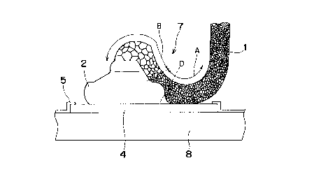
As shown in Fig. 1, a part B immediately above
the metallic ball 2 where crystal grains are turned coarse
because of thermal influences by the discharging is
generated only inside a position D where the metallic wire
1 is to be pulled and broken, in other words, inside a
boundary D of the bonding between the metallic ball 2 and
metallic wire 1.
Owing to this, a crystal grain structure of the
metallic wire 1 behind the position D where the metallic
wire 1 is to be pulled and broken becomes uniform and thus
a breaking load becomes constant, whereby the metallic wire
1 is broken starting from the position D to be pulled and
broken where the metallic wire is pressed by the capillary
and consequently reduced in sectional area. In other words,
the ~etallic wire 1 is broken always at the position D to
be pulled and broken, thus forming the two-staged
projecting bump 7 of a uniform shape.
For example, in the case where the metallic ball
2 of an original diameter 60um is made and then the two-
staged projecting bump 7 is formed which has the metallic
ball 2 of an approximately 80um diameter (a pedestal
diameter) after bonded onto the electrode 4 of the
semiconductor element 8, a length from immediately above
the metallic ball 2 to the position D to be pulled and
broken, more specifically, to the position D where the
bonding of the metallic ball 2 and metallic wire 1
CA 022~2102 1998-10-16
terminates is approximately 80um.
Fig. 2 shows a formation ratio of defective two-
staged projecting bumps 7a having an excess of the metallic
wire 1 left as shown in Fig. 16 among the two-staged
projecting bumps formed by changing the length from
immediately above the metallic ball 2 to the part B where
the crystal grains become coarse because of the thermal
influences by the discharging. Fig. 2 is obtained from
average data of 4800 bumps.
In Fig. 2, an axis of abscissa represents the
length from immediately above the metallic ball 2 to the
part B where the crystal grains become coarse because of
the thermal influences of the discharging, and an axis of
ordinate shows the formation ratio of two-staged projecting
bumps with the excessive metallic wire 1 left.
As is found from Fig. 2, if the length from
immediately above the metallic ball 2 to the part B where
the crystal grains become coarse because of the thermal
influences of the discharging is not larger than
approximately 80um, no defective two-staged projecting bump
with the excessive metallic wire 1 left is brought about.
The above value of approximately 80um corresponds to the
length from immediately above the metallic ball 2 to the
position D where the metallic wire 1 is to be pulled and
broken, namely, to the position D where the bonding of the
~etallic ball 2 and metallic wire 1 terminates.
In other words, when the part B right above the
~etallic ball 2 where the crystal grains become coarse
CA 022~2102 1998-10-16
because of the thermal influences of the discharging does
not exceed the position D where the metallic wire 1 is to
be pulled and broken, i.e., within the boundary D where the
bonding of the metallic ball 2 to the metallic wire 1
S terminates, the two-staged projecting bump 7 can be formed
in the normal shape at all times. Since a uniform amount
of a conductive paste can be transferred process to the
two-staged projecting bumps 7 in the succeeding process,
the reliability for mounting the semiconductor element to a
circuit board is improved.
(Working Example 1)
Firstly, a concrete example wherein the process
of melting the leading end of the metallic wire 1 thereby
- forming the metallic ball 2 to the leading end of the
metallic wire 1 which are different from the prior art will
be depicted here.
As shown in Fig. 3, in forming the metallic ball
2 through discharging between the leading end of the
metallic wire 1 passed through the capillary 3 and an
electrode 6, an amount of an energy applied to the leading
end of the metallic wire 1 is equal to (a current value)x(a
voltage value)x(a discharging time). In this case, while
the voltage value is determined by a distance F between
leading ends of the electrode 6 and metallic wire 1, the
voltage value can be considered constant at all times
because the distance F is always constant at the
discharging time. Therefore, the applied energy, that is,
a diameter of the for~ed metallic ball 2 is proportional to
CA 022~2102 1998-10-16
the discharging time and current value, although countless
combinations of the discharging time and current value are
conceivable to form metallic balls 2 of the same diameter.
However, among the above two parameters in
discharging, namely, the discharging time and current value,
what influences a length of an area of the metallic wire
where the crystal grains become coarse due to the thermal
influences by the discharging is the discharging time. Fig.
4 is a graph of a relationship of the discharging time on
an axis of abscissa and a distance represented on an axis
of ordinate from immediately above the metallic ball 2 to
the area where the crystal grains are coarse. In this case,
the-metallic ball is formed in a diameter of 60um and, the
current value and voltage value are 40mA and 900V. Fig. 4
is average data of 1120 bumps.
It is found from Fig. 4 that the length of the
area where the crystal grains become coarse is proportional
to the discharging time, and that the shorter the
discharging time is, the shorter becomes the area length.
Meanwhile, the formation ratio of the defective
two-staged projecting bumps 7a is proportional to the
length of the area where the crystal grains become coarse,
as confirmed from Fig. 2. Therefore, the two-staged
projecting bumps 7 in the normal shape of Fig. 1 can be
obtained with good reproducibility if the discharging time
is controlled so as to set the length of the area where the
crystal grains become coarse to such a length not as to
cause the defective two-staged projecting bumps 7a with the
CA 022~2102 1998-10-16
excessive metallic wire 1 left.
For instance, when the metallic ball 2 having an
original diameter of 60um is made and bonded onto the
electrode 4 of the semiconductor element 8 to have
approximately 80~m diameter (pedestal diameter) in the two-
staged projecting bump 7, if the length of the area where
the crystal grains become coarse is made not larger than
approximately 80~m, the defective two-staged projecting
bump 7a is avoided.
The above value of approximately 80um corresponds
to the length from immediately above the metallic ball 2 to
the part D to be pulled and broken, namely, to the
termination part D of the bonding between the metallic ball
2 and metallic wire 1. Therefore, if the metallic ball is
formed in not longer than lms discharging time, the area
length where the crystal grains are rough is restricted to
80um or shorter, thereby realizing the normal two-staged
projecting bumps 7 with good reproducibility.
In Fig. 5, the axis of abscissa represents the
discharging time and the axis of ordinate represents the
formation ratio of the defective-two-staged projecting
bumps 7a having the excessive metallic wire left. From
this Fig. 5, it is found that when the length of the area
where the crystal grains become coarse is controlled by the
discharging time so as to set the length to a length not to
bring about the defective two-staged projecting bumps 7a
with the excessive metallic wire 1 left, specifically, a
length not larger than the length from immediately above
CA 022~2102 1998-10-16
24
the metallic ball 2 to the part D to be pulled and broken,
i.e., to the terminating part D of the bonding between the
metallic ball 2 and metallic wire 1, the two-staged
projecting bumps 7 in the normal shape can be formed with
good reproducibility.
It is accordingly important to select such a
discharging time that the part B where the crystal grains
become coarse due to the thermal influence by the
discharging is accommodated in length within the area from
immediately above the metallic ball 2 to the part D where
the metallic wire 1 is to be pulled and broken in Fig. 1,
to form the metallic ball 2.
(Working Example 2)
This working example 2 is a concrete example
wherein the processes of pressing and bonding the formed
metallic ball 2 to the electrode 4 are different from the
prior art. Fig. 6B shows a state immediately before the
metallic wire 1 is pulled and broken at the final process.
In stead of controlling the discharging time when
the metallic ball 2 is formed as in the previous working
example 1, a pressure, a pressing speed, a bonding time, a
bonding temperature, etc. when the metallic ball 2 is
bonded to the electrode 4 of the semiconductor element 8
are controlled, thereby positioning the part B where the
crystal grains are turned coarse because of the thermal
influences at the forming time of the metallic ball 2
inside the boundary D where the bonding of the metallic
ball 2 to the metallic wire 1 terminates, in the same
CA 022~2102 1998-10-16
fashion as in the two-staged projecting bump shown in Fig.
1. Such positioning is carried out by the following method.
The method will be discussed with reference to
Figs. 6A and 6B.
In order to form the two-staged projecting bumps
shown in Figs. 6A, 6B, metallic wires 1 are used which have
the same length as the length from immediately above the
metallic ball 2 which has been formed to the part B
(referring to Fig. 13) where the crystal grains become
coarse due to the thermal influence by the discharging.
However, the diameter (pedestal diameter) of the metallic
ball 2 after the two-staged projecting bump is formed is
different between Figs. 6A and 6B.
The pedestal diameter in the example of Fig. 6A
is G, while that in the example of Fig. 6B is H. G<H is
held. In the two-staged projecting bumps of Figs. 6A and
6B, the part B where the crystal grains become coarse under
the thermal influences of the discharging from immediately
above the metallic ball 2 expands beyond the part D to be
pulled and broken, i.e., the terminating position D of the
bonding between the metallic ball 2 and metallic wire 1.
To the contrary, in the example of Fig. 6B, the part B
where the crystal grains become coarse under the thermal
influences of the discharging from immediately above the
metallic ball 2 is accommodated inside the part D to be
pulled and broken.
From the result of Fig. 2, therefore, the
defective two-staged projecting bump 7a with the excessive
CA 022~2102 1998-10-16
26
metallic wire 1 left is produced in the shape of Fig. 6A,
whereas the good two-staged projecting bump without the
excessive metallic wire 1 left is obtained in the shape of
Fig. 6B.
As above, the length from immediately above the
metallic ball 2 to the part D to be pulled and broken, that
is, the part D where the bonding of the metallic ball 2 and
metallic wire 1 terminates can be controlled by the
pedestal diameter of the two-staged projecting bump. So
long as the shape is so designed that the part where the
crystal grains become coarse and the breaking strength is
reduced to nearly half is arranged to be inside the part D,
the defective two-staged projecting bump 7a can be
prevented. And the pedestal diameter is controllable by
the pressure, pressing speed, bonding time, bonding
temperature, etc., when the metallic ball is bonded to the
electrode 4 of the semiconductor element 8.
[SECOND EMBODIMENT]
A bump and a method for forming the same
according to a second embodiment will be described with
reference to Figs. 7-9.
The two-staged projecting bump of the second
embodiment is formed basically in the same procedures as
indicated in Figs. 12A-12F. That is, while a high voltage
is applied between the leading end of the metallic wire 1
passed through the capillary 3 and the electrode, the
leading end of the metallic wire 1 is melted by the energy
generated by the discharge, thereby forming the metallic
CA 022~2102 1998-10-16
ball 2 at the leading end thereof. The capillary 3 is
~oved to position the metallic ball 2 on the electrode 4 of
the semiconductor element 8. The metallic ball 2 is bonded
to the electrode 4 by thermocompression bonding or
ultrasonic thermocompression bonding. Then the capillary 3
is raised, moved sideways and descended. The metallic wire
1 is bonded to the metallic ball 2 bonded to the electrode
4 by thermocompression bonding or ultrasonic
thermocompression bonding. Thereafter, the capillary 3 is
raised again and the metallic wire 1 is pulled and broken
with the metallic ball 2 left in the bonded state to the
electrode 4. In the process, a two-staged projecting bump
is formed on the electrode 4.
In the above-described process, when the metallic
~all 2 is bonded to the electrode 4 of the semiconductor
element 8, and the capillary 3 is moved up and sideways,
then moved down so as to bond the metallic wire 1 onto the
~etallic ball 2 bonded to the electrode 4, the metallic
wire 1 is caught between the electrode 4 of the
semiconductor element 8 or the semiconductor element itself
and the capillary 3 as denoted by E parts in Fig. 7. As a
result, the neck 14 is generated in the metallic wire 1 as
in Fig. 20, enabling the formation of the two-staged
projecting bump 7 of good shape. The process will be
detailed hereinbelow.
A hardness of the metallic wire 1 at the E part
where the neck 14 is formed, that is, a hardness of a part
of the metallic wire which has a distance I from
CA 022~2102 1998-10-16
28
immediately above the metallic ball 2 iS set to be not
smaller than 2/3 a hardness of the metallic wire at a part
not thermally influenced by the discharge.
In this case, a size of the neck 14 generated in
the metallic wire 1 due to the pressing by the capillary 3
is dependent on the hardness of the metallic wire 1 of the
neck part. The smaller the hardness, the bigger the neck
is. On the other hand, the size of the neck 14 influences
the breaking load thereat. The bigger the neck 14 is, the
smaller the breaking load is. If the hardness of the part
of the metallic wire where the neck 14 is formed, in other
words, the hardness of the part of the metallic wire 1
spaced the distance I from immediately above the metallic
ball 2 iS not smaller than 2/3 the hardness of the metallic
wire of the part not thermally influenced by the
discharging, a breaking strength of the neck part 14 (E
part) with the break starting from the size of the neck 14
formed at the hardness becomes larger than a breaking
strength of the part D where the metallic wire 1 is to be
pulled and broken, that is, the boundary D where the
bonding between the metallic ball 2 and metallic wire 1
terminates. Then, the metallic wire 1 is broken at the
position D to be pulled and broken at all times, thus
producing the two-staged projecting bump 7 of uniform shape.
Fig. 8 is a graph of a relationship of the
hardness of the part where the neck 14 is formed which is
indicated on an axis of abscissa and the formation ratio of
defective two-staged projecting bumps 7a with the remaining
CA 022~2102 1998-10-16
29
excessive metallic wire 1 which is represented on an axis
of ordinate. The part of the metallic wire 1 used in the
experiment and not thermally influenced by the discharging
has a Vickers hardness of 80Hv. It is found from Fig. 8
that if the hardness of the part where the neck 14 is
formed is not smaller than 3/4=(60Hv/80Hv) the hardness of
the not-thermally-influenced part of the metallic wire, the
defective two-staged projecting bump 7a is not given rise
to. However, since the size of the neck 14 varies
depending on a shape of the capillary 3 and bonding
conditions, the hardness of the E part is set to be 2/3 or
larger than the hardness of the not-thermally-influenced
part to leave some margin.
Accordingly, the amount of the conductive paste
transferred to each two-staged projecting bump in the next
process becomes uniform, and therefore the semiconductor
element is mounted to the circuit board with improved
reliability.
Hereinbelow will be described based on Fig. 9 a
method for forming the two-staged projecting bump wherein
the hardness of the E part of the metallic wire 1 where the
neck 14 is formed, namely, the hardness of the part spaced
by the distance I from immediately above the metallic ball
2 is not smaller than 2/3 the hardness of the not thermally
influenced part of the metallic wire 1.
Fig. 9 is a graph of a hardness distribution of
the metallic wire 1 measured in its longitudinal direction
from immediately above the metallic ball 2 after the
, .. .... . . . .. .
CA 022~2102 1998-10-16
metallic ball 2 is formed to the leadlng end of the
metallic wire 1 by the discharging. From this Fig. 9, the
hardness of the part B where crystal grains are made coarse
because of thermal influences by the discharging is
increased as a distance of the part B is increased from
immediately above the metallic ball 2. Therefore, the
distance of the B part should be shortened so as to set
high the hardness of the I part where the neck 14 is formed
by the pressing of the capillary 3.
That is, when the metallic ball 2 is formed, the
length of the B part should be controlled so that the
hardness of the I part is 2/3 or larger than the original
hardness of the metallic wire 1 without thermal influences.
And, the length of the B part of coarse crystal grains can
be controlled by the discharging time. Specifically, when
the metallic ball 2 is formed, such discharging time that
makes the hardness of the I part not smaller than 2/3 the
original hardness of the metallic wire 1 without being
thermally influenced should be selected to form the
metallic ball 2.
[THIRD EMBODIMENT]
Figs. 10-llF indicate a bump and a method for
forming the bump according to a third embodiment.
Fig. 10 illustrates a state immediately before
the metallic wire 1 is pulled and broken at the final step
of the process in the two-staged projecting bump of the
third embodiment. Although the process proceeds in the
same manner as in the first and second embodiments until
CA 022~2102 1998-10-16
the metallic ball 2 is bonded to the electrode 4, the
metallic wire 1 immediately above the metallic ball 2 is
finished in a loop J according to the third embodiment. In
other words, the bump includes the loop-shaped part J where
the metallic ball 2 and metallic wire 1 are not bonded with
each other.
In the embodiment, since the metallic wire 1
immediately above the metallic ball 2 is in the loop shape,
a distance D from immediately above the metallic ball 2 to
a position D where the metallic wire 1 is to be pulled and
broken, that is, to an edge part of the metallic ball 2
bonded onto the electrode 4 of the semiconductor element 8
can be secured optionally long. Therefore, the metallic
wire area B where the crystal grains are thermally
influenced by the discharge and turned coarse can be
accommodated inside the position D where the metallic wire
1 is to be pulled and broken. The metallic wire 1 is
accordingly surely broken at the position D to be pulled
and broken at all times, so that the two-staged projecting
bump is for~ed in uniform shape.
In the process wherein the metallic ball 2 is
bonded to the electrode 4 of the semiconductor element 8
and, the capillary 3 is raised, moved sideways and lowered
to bond the metallic wire 1 to the metallic ball 2 bonded
to the electrode 4 by thermocompression bonding or
ultrasonic thermocompression bonding, as shown in Figs. 7
and 20, even if the metallic wire 1 is caught between the
electrode 4 of the semiconductor element 8 or semiconductor
CA 022~2102 1998-10-16
element 8 itself and the capillary 3 thereby to bring about
the neck 14, because of the provision of the loop shape,
the distance I from immediately above the metallic ball 2
to the neck 19 can be adjusted by optionally changing the
S loop shape. Then, the hardness of the metallic wire 1 of
the neck 14 formed by the pressing of the capillary 3 can
be controlled to be not smaller than 2/3 the hardness of
the metallic wire not thermally influenced by the
discharging. Accordingly, the metallic wire 1 can be
broken always at the position D to be pulled and broken and
the two-staged projecting bump is obtained in uniform shape.
For forming the normal two-staged projecting bump,
a combined way of control may be performed in addition to
the control of the loop shape, for example, a control to
the length of the B part where the crystal grains are
turned coarse because of thermal influences by the
discharging time, a control by the pedestal diameter of the
bump to the length from immediately above the metallic ball
to the part D where the metallic wire is to be pulled and
broken, etc. may be combined.
Figs. llA-llF show a process of forming the two-
staged projecting bump having the loop part J.
First, as shown in Fig. llA, the metallic wire 1
of gold, copper, aluminum, solder or the like is passed
through the capillary 3 of ceramic or ruby. The leading
end of the passed metallic wire 1 and an electrode 6 as a
torch are discharged therebetween, thereby forming the
metallic ball 2.
CA 022~2102 1998-10-16
In Fig. llB, the metallic ball 2 is pressed on
the preheated electrode 4 of the semiconductor element 8,
to which ultrasonic vibrations are applied. The metallic
ball 2 is bonded to the electrode 4 by the action of the
temperature, pressure, and ultrasonic vibrations. A
reference numeral 5 is a passivation film for protecting an
active face of the semiconductor element 8.
In Fig. llC, the capillary 3 is moved to a
direction apart from a moving direction thereof when the
metallic wire 1 is bonded to the metallic ball 2 in Fig.
llD, so as to describe a circular locus or an elliptic
locus.
The loop part J is formed by the metallic wire 1
through the movement of the capillary 3 in Figs. llC and
llD. In Fig. llD, the metallic wire 1 is brought in touch
with the metallic ball 2 and bonded to the metallic ball 2
by the action of the temperature and pressure or by the
action of the temperature, pressure and ultrasonic
vibrations. Thereafter, as shown in Fig. llE, the
capillary 3 is raised. The metallic wire 1 is pulled and
broken as shown in Fig. llF, whereby the two-staged
projecting bump is completely formed.
In the two-staged projecting bump of the
semiconductor element and the method for forming the bump
of the present invention, the area (recrystallized area)
immediately above the metallic ball of the metallic wire
for forming the two-staged projecting bump on the electrode
of the semiconductor element where the crystal grain
CA 022~2102 1998-10-16
34
structure is turned coarse because of thermal influences by
the discharge is set not to exceed the distance from
immediately above the metallic ball to the part where the
metallic wire is to be pulled and broken, in other words,
the area is set to be accommodated inside the boundary of
the bonding between the metallic wire and metallic ball.
Therefore, the metallic wire is always broken at the
position to be pulled and broken, and then, the two-staged
projecting bump can be formed in uniform shape.
Along with the above-described effect, when the
conductive paste is transferred onto the thus-formed two-
staged projecting bumps by a transfer method, the amount of
the conductive paste trans~erred to each bump is less
varied, so that the bonding reliability when the
semiconductor element is mounted to the circuit board is
improved.
The entire disclosure of Japanese Patent
Application No. 8-95774 filed on April 18, 1996, including
specification, claims, drawings, and summary are
incorporated herein by reference in its entirety.
Although the present invention has been fully
described in connection with the preferred embodiments
thereof with reference to the accompanying drawings, it is
to be noted that various changes and modifications are
apparent to those skilled in the art. Such changes and
modifications are to be understood as included within the
scope of the present invention as defined by the appended
claims unless they depart therefrom.