Note: Descriptions are shown in the official language in which they were submitted.
CA 02252810 1998-10-28
WO 97!42583 PCT/US97/05610
SYSTEM AND METHOD FOR GENERATING FRACTIONAL LENGTH
DELAY LINES IN A DIGITAL SIGNAL PROCESSING SYSTEM
The present invention relates generally to digital signal processing for
generating music and other digitally sampled signals, and particularly to the
use of delay lines having non-integer lengths in digital signal processing
systems and methods.
BACKGROUND OF THE INVENTION
The development of high quality Digital Waveguide, Karplus-Strong, and
Commuted Synthesis musical instrument synthesis techniques requires the
use of delay fines with non-integer lengths in a feedback loop arrangement.
Required features of these delay lines are:
The delay line lengths must be smoothly variable by some controlling
signal in order to model pitch bend, glissando, and vibrato effects.
Pitchbend is a required feature for all instruments complying with the
general MIDI standard.
CA 02252810 1998-10-28
WO 97/42583 PCT/US97/05610
-2-
The delay lines must have a flat unity gain frequency response to
minimize energy loss in the feedback loop. Musical notes generated
by a resonating feedback loop containing a delay fine that does not
have a unity gain frequency response may exhibit undesirable energy
loss and decay away too quickly.
No standard methods for interpolation of non-integer length delay lines are
generally known that have both of these required features. Referring to Fig.
1, there is shown a "Karplus-Strong delay line" 50 that includes a sampled
data delay line 52, a linear interpolation filter 54, and a feedback path 56.
The sampled data delay line 52 stores one digitally sampled data value for
each sampling period. For instance, if the system in which the delay tine 50
is used has a sampling rate fs of 44,100 Hz, then a new data sample is
inserted into the delay line 44,100 times per second. If data is simply read
from the delay tine at specified reader position R, producing an output signal
denoted as UR(n}, then the delay line is said to be an integer length delay
line, because the output signal UR(n) is delayed by an integer number of
sampling periods from the time it was input into the delay line.
In the Karplus-Strong delay line 50, a linear interpolation is performed so as
to produce a delay line having a fractional length of L + a0, where L is an
integer and a0 is a fractional value between 0 and 1. L is the distance, in
units of data sample positions, between the current input position W to the
delay line and the filter's reader position, R-1, during the prior sample
period:
L=R- 1 -W.
During each time period, n, the filter 54 reads a sampled data value UR(n}
and outputs a filtered data value out(n) that is computed as follows:
out(n) = a0 x UR(n) + (1- a0) x UR(n-1).
CA 02252810 1998-10-28
WO 97/42583 PCT/US97105610
-3-
For example, if a0 is set equal to 0.5, the delay fine has an effective length
of
L + 0.5, and out(n) is equal to the average of the two data samples most
recently read by the filter:
out(n) = 0.5 x (UR(n) + UR(n-1 ).
Non-integer length delay lines such as the Karplus-Strong delay line 50 that
use linear interpolation, or other FIR (finite impulse response filter)
interpolation methods, can be varied smoothly in length by a control signal
(e.g., a0 in the delay line shown in Fig. 1 ), but they have unsatisfactory
energy losses caused by the FIR interpolation filter itself in high frequency
(short delay length) loops. This causes high pitched musical notes to decay
away too quickly. For instance, when the control coefficient a0 is set to 0.5
in
the Karplus-Strong delay line 50, the filter 54 acts as a low-pass filter with
a
cut-off frequency of half the sampling rate and also substantially attenuates
frequency components of the loop signal that are close to the cut-off
frequency.
On the other hand, standard allpass filter interpolation solves this problem
for
the static case (i.e., where the reader position and filter coefficients
remain
constant). See David A. Jaffe and Julius O. Smith III, "Extensions of the
Karplus-Strong Plucked-String Algorithm", Computer Music Journal 7(2):
56-69, 1983 (hereinafter "Jaffe and Smith 1983"). Figs. 2 and 3 show a delay
line with an allpass filter interpolator 70. This delay line 70 includes a
sampled data delay line 52, an allpass interpolation filter 72, and a feedback
path 56. As shown in Fig. 3, the allpass filter 72 includes two adders 74, 75,
one multiplier 76 and two unitary delay elements 77, 78. During each time
period, n, the allpass filter 72 reads a sampled data value UR(n) and outputs
a filtered data value out(n) that is computed as follows:
out(n) = UR(n-1 ) + AP COEF x ( UR(n) - out(n-1 ) ).
CA 02252810 1998-10-28
WO 97/42583 PCT/US97/05610
-4-
So long as the position of the delay line read pointer for the allpass filter
72
remains unchanged, and the filter coefficient AP COEF remains unchanged,
this filter preserves the energy in the sampled loop signal. However, when
implementing pitch bend, glissando, or vibrato effects, the allpass filters in
delay lines using allpass filter interpolation introduce undesirable
artifacts,
such as audible clicks. This is primarily due to the internal state in the
filter
72, which must be handled carefully when changing the filter's coefficient
and/or the position of the delay line read pointer. Until now it has been
necessary to chose between unity gain in loops (using allpass filter
interpolation) and flexibility of loop length control (using linear filter or
FIR
filter interpolation).
It is therefore a goal of the present invention to provide a new delay line
interpolation structure that has the time-varying delay-length flexibility of
simple linear interpolation of a delay line, while retaining the energy
conserving effects and quality of static allpass interpolation.
Another object of the present invention is to provide a delay line
interpolation
structure that is computationally efficient.
SUMMARY OF THE INVENTION
In summary, the present invention is a sampled data, non-integer delay tine
interpolation structure that includes a sampled data delay line, two allpass
filters, each having an associated read pointer for reading data at a
corresponding integer position of the delay line, an alternating crossfader
that
alternatingly crossfades between the outputs of the two allpass filters, plus
a
controller that controls when the read positions of each allpass filter is
updated and also controls when the filter coefficient of each allpass filter
is
updated.
CA 02252810 1998-10-28
WO 97/42583 PCT/US97/05610
_5_
The controller receives a control signal indicating a specified delay fine
length that is to be implemented by the delay line interpolation structure.
The
specified delay length is sampled by the controller each time the crossfade
orientation of the alternating crossfader is changed, and from that value the
controller generates a new read pointer and filter coefficient for allpass
filter
to which the structure will next crossfade. The new read pointer is an integer
that corresponds to an integer portion of the specified delay length, and the
filter coefficient corresponds to a fractional portion of the specified delay
length. After updating the read pointer and filter coefficient of one of the
two
allpass filters, the alternating crossfader outputs the signal generated by
the
other allpass filter for a first number of sample periods until the updated
filter
"warms up." Then the alternating crossfader crossfades to the signal
generated by the updated allpass filter over a second number of sample
periods.
At the end of each crossfade operation, at which point the crossfader has
crossfaded completely or almost completely to the signal generated by one of
the allpass filters, the specified delay line length is sampled again, the
reader
position and filter coefficient of the other allpass filter are updated, and
then
the crossfade operation repeats.
By providing a warm up period after each filter update, the generation of
transient signals unrelated to the signal in the delay line is avoided.
Furthermore, the technique of gradually crossfading between two allpass
filters preserves the energy of the signals in the delay line while providing
smooth transitions from one delay line length to another.
CA 02252810 2004-07-28
14673-11
-5a-
The invention may be summarized according to a
first aspect as a sampled data, non-integer delay line
interpolation structure, comprising: a sampled data delay
line having a multiplicity of integer positions at which
data is stored; first and second allpass filters, each
having an associated read pointer for reading data at a
corresponding integer position of the delay line, each
allpass filter generating an associated output in accordance
with a filter coefficient assigned thereto and the data read
from the delay line; a controller that assigns to each
allpass filter's read pointer a respective delay line
position and assigns to each allpass filter a respective
filter coefficient value, wherein the delay line position
and filter coefficient assigned to each allpass filter
together corresponding to a respective effective delay line
position for each allpass filter; and a crossfader that
smoothly crossfades between the outputs of the first and
second allpass filters so as to generate an output signal
that corresponds to a delay line read position that smoothly
transitions from a first effective delay line position to a
second effective delay line position.
According to another aspect the invention provides
a method of delaying digitally sampled data by a smoothly
varying non-integer number of delay periods, comprising the
steps of: storing digitized data in a sampled data delay
line having a multiplicity of integer positions at which
data is stored; filtering data from the delay line with
first and second allpass filters, each having an associated
read pointer for reading data at a corresponding integer
position of the delay line, each allpass filter generating
an associated output in accordance with a filter coefficient
assigned thereto and the data read from the delay line;
assigning to each allpass filter's read pointer a respective
CA 02252810 2004-07-28
74673-11
-5b-
delay line position and assigning to each allpass filter a
respective filter coefficient value, wherein the delay line
position and filter coefficient assigned to each allpass
filter together corresponding to a respective effective
delay line position for each allpass filter; and smoothly
crossfading between the outputs of the first and second
allpass filters so as to generate an output signal that
corresponds to a delay line read position that smoothly
transitions from a first effective delay line position to a
second effective delay line position.
According to a further aspect the invention
provides a signal processing system, comprising: a data
processor; memory coupled to the data processor for storing
data structures and instructions to be executed by the data
processor; the data structures stored in the memory
including a sampled data delay line having a multiplicity of
integer positions at which data is stored; the instructions
stored in the memory including: filtering instructions
implementing two allpass filters, each having an associated
read pointer for reading data at a corresponding integer
position of the delay line, each allpass filter generating
an associated output in accordance with a filter coefficient
assigned thereto and the data read from the delay line;
control instructions for assigning to each allpass filter's
read pointer a respective delay line position and assigning
to each allpass filter a respective filter coefficient
value, wherein the delay line position and filter
coefficient assigned to each allpass filter together
corresponding to a respective effective delay line position
for each allpass filter; and crossfade instructions that
generate an output signal that smoothly crossfades between
the outputs of the first and second allpass filters, the
output signal corresponding to a delay line read position
CA 02252810 2005-O1-04
74673-11
_~o_
that smoothly transitions from a first effective delay line
position to a second effective delay line position,
CA 02252810 1998-10-28
WO 97/42583 PCT/US97/05610
-6-
BRIEF DESCRIPTION OF THE DRAWINGS
Additional objects and features of the invention will be more readily apparent
from the following detailed description and appended claims when taken in
conjunction with the drawings, in which:
Fig. 1 is a schematic representation of a delay line with a linear
interpolator
filter.
Fig. 2 is a schematic representation of a delay line with an allpass filter
interpolator.
Fig. 3 is a schematic representation of an allpass filter.
Fig. 4 is a block diagram of a computer system implementing a preferred
embodiment of the present invention.
Fig. 5 is a schematic representation of a delay line with a preferred
embodiment of the dual allpass filter interpolator with alternating crossfader
of the present invention.
Fig. 6 is a timing diagram representing the operation of the alternating
crossfader in a preferred embodiment of the present invention.
DESCRIPTION OF THE PREFERRED EMBODIMENTS
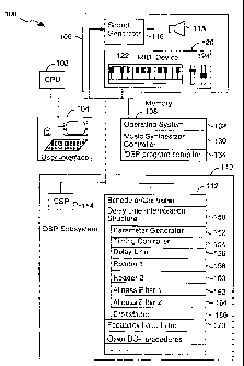
Referring to Fig. 4, there is shown a computer-based music synthesis system
100 having a host CPU 102, a computer user interface 104, a music interface
106, memory 108 (including fast random access memory and non volatile
memory such as disk storage), and a digital signal processor (DSP)
subsystem 110.
CA 02252810 1998-10-28
WO 97/42583 PCT/US97/05610
The DSP subsystem 110 executes DSP programs downloaded by the host
CPU 102 into the DSP subsystem's memory 112. The downloaded DSP
programs typically are music synthesis programs that, when executed by the
DSP subsystem's processor 114 (typically called a DSP), generate audio
frequency signals. Those output signals constitute a stream of digital data
values that are converted by a sound generator 116 (in the music interface)
into analog electrical signals that are then converted into audible sound by a
speaker 118. Control signals used by the DSP 114 when executing the DSP
programs can originate from a MIDI device 120, such as a device having a
keyboard 122 and one or more pitch blend wheels 124, of from a computer
keyboard or pointing device in the computer user interface 106. Input signals
from these input devices are typically pre-processed by the host CPU 104
through the execution of a music synthesizer control program 130 to produce
a control parameter that is then passed to the DSP subsystem 110.
In addition to the music synthesizer control program 130, the host CPU's
memory 108 also will typically store an operating system 132, a DSP program
compiler 134, as well as other software and data that are not directly
relevant
to the present discussion.
The memory 112 in the DSP subsystem 110 typically stores compiled DSP
procedures 150, 170, and a scheduler or controller program 140 that
schedules the execution of all the DSP procedures 150, 170 being executed
by the DSP 114. The only one of those DSP procedures that is directly
relevant to the present invention is the delay line interpolation structure
procedure 150, which is schematically represented in Fig. 5.
While for ease of explanation the delay line interpolation structure 150 will
be
discussed as though it were a physical electronic circuit, it is in fact
generally
implemented as a DSP program or procedure. Actual music synthesis
systems using the present invention will typically use delay line
interpolation
structures 150 wherever delay lines of non-integer length are needed, and
CA 02252810 1998-10-28
WO 97/42583 PCT/US97/05610
_g_
thus such systems will often have a plurality of delay line interpolation
structures.
The delay line interpolation structure 150 includes a parameter generator
152, a timing controller 154, a delay line 156, first and second delay line
readers 158, 160, two allpass filter interpolators 162, 164, and an
alternating
cross fader 166. As will become clear from the discussion below, the two
delay line readers 158, 160 may be considered to be part of their respective
all pass filters. The parameter generator 152 and timing controller 154 may
be considered to compose the delay line interpolation structure's controller.
The delay line's AUDIO IN and AUDIO OUT signals, which are also labeled
u1 (n) and u6(n), respectively, are the input and output audio signal to and
from the delay line 156. These signals are updated at the audio sampling
rate, for example 44,100 Hz or 22,050 Hz. In the preferred embodiment the
audio sampling rate is 44,100 Hz.
DLEN is the input signal that controls the fractional delay line length. This
signal may operate at the audio sampling rate, at some slower control rate, or
at any asynchronous rate. It may be pre-processed to the desired control
rate, or just left to the timing controller 154 to synchronize with the audio
signal rate.
The signals marked u1 (n), u2(n),...,u6(n) are internal signals; n is the
audio
sampling index. Thus, u1 (n) represents the value of signal ui at time sample
period n, while u1 (n-1 ) represents the value of signal u1 at time sample
period n-1.
For the purposes of explaining the operation of the preferred embodiment of
the present invention, we will assume that the host CPU 104 receives a pitch
signal fBW from one of the pitch blend wheels 124 and generates a "delay
CA 02252810 1998-10-28
WO 97/42583 PCT/US97/05610
_g_
length" value DLEN that is equal to the DSP subsystem's data sampling rate
(typically 44,100 Hz) divided by the pitch signal:
DLEN = sampling rate I pitch
= 44,100 / fB~,
For instance, if fBW is equal to 220 Hz, then DLEN is equal to 200.4545
samples.
The parameter generator 152 converts the delay length value DLEN received
from the host CPU into an associated integer value DLEN_INT and a filter
coefficient AP COEF. As indicated, DLEN is a real number that may not be
an integer.
For the purposes of this document, the term "crossfade" is defined to mean
combining two signals so as to smoothly transition from one signal to the
other. For instance, given two signals S1 and S2, a crossfade signal CF may
be defined as:
CF = a~S1 + (1-a)~S2
where a is the "crossfade" coefficient. As a is smoothly transitioned in value
from 0 to 1, the signal CF crossfades (i.e., smoothly transitions) from a
value
corresponding to S2 to a value corresponding to S1.
The delay line 156, as described above with reference to Fig. 1, stores and
delays a digital audio signal by an integral number of time samples. The
integer number of time sample delays is determined by the read pointer
positions of reader 1 and reader 2. The delay line is generally formed by the
combination of sequential data memory locations and an addressing scheme
constructed such that an audio signal sample may be stored in the memory
and read back out at a specified number of integral time samples later. The
CA 02252810 1998-10-28
WO 97/42583 PCT/US97/05610
-10-
delay line data structure is constructed in the preferred embodiment such that
there may be more than one reader, and such that the delay time intervals
(i.e., read pointer positions} associated with each reader may be changed
arbitrarily whenever the timing controller 154 indicates that a crossfade
orientation change must occur. In the preferred embodiment, the delay line is
implemented using a circular buffer design (i.e., an array of memory
locations) with separate read and write pointers.
In the preferred embodiment, the read pointer positions of the readers
changes no more frequently than every T samples, where T is the minimum
crossfading time interval allowed. For instance, when T is set to 16,
alternating ones of the read pointer positions are updated no more frequently
than every 16 sample periods.
The delay line 156 in combination with reader 1 delay the AUDIO IN signal by
DLEN_INT1 time samples as follows,
u2(n) = u1 (n - DLEN_INT1)
The delay line 156 in combination with reader 2 delay the AUDIO IN signal by
DLEN_INT2 time samples as follows,
u4(n) = u1 (n - DLEN_INT2)
The first allpass filter AP1 is a standard first order allpass filter, the
output of
which may be computed in a variety. of ways that are generally known, in
particular by the following difference equation,
u3(n) = AP COEF1 x u2(n) + u2(n-1 ) - AP COEF1 x u3(n-1 )
CA 02252810 1998-10-28
WO 97/42583 PCT/US97/05610
-11 -
The second allpass filter AP2 is also a standard first order allpass filter,
the
output of which may be computed in a variety of ways that are generally
known, in particular by the following difference equation,
u5(n) = AP_COEF2 x u4(n) + u4(n-1 ) - AP COEF2 x u5(n-1 )
The parameter generator 152 takes a positive non-integer delay line length
input value, DLEN, and converts it to a integer part, DLEN_INT, and a
fractional part, DLEN_FRAC, which may be greater than 1Ø DLEN_INT is
used to set the length of an integer length delay line, while DLEN_FRAC is
converted to the appropriate allpass filter coefficient, AP COEF, to
implement the fractional delay portion as a first order allpass filter. The
integer delay line and the first order allpass filter cascaded together then
implement the non-integer delay line length, DLEN.
It is known that a first order allpass filter may be used to implement
fractional
delays. The first order allpass filter may be computed by the following
difference equation, which is equivalent to equations for the allpass filters
shown above:
Output(n) = AP COEF x Input(n) + Input(n-1 ) -
AP_COEF x Output(n-1 },
where Input(n) and Output(n) are the time sample indexed input and output
signals to the allpass filter, respectively, and AP COEF is the allpass filter
coefficient.
There are a variety of methods for generating the exact or approximated
allpass filter coefficient for a desired fractional delay length. Jaffe and
Smith
(1983) note that -
AP COEF = (1 - DLEN FRAC) / (1+DLEN_FRAC)
CA 02252810 1998-10-28
WO 97/42583 PCT/US97/05610
-12-
makes a very good approximation the desired allpass filter coefficient to
implement a fraction delay of DLEN_FRAC time samples. Since a divide
operation is required in the above computation, and since divide operations
are generally difficult to perform using many DSP's, in the preferred
embodiment an alternative polynomial series approximation, derived from a
Taylor Series expansion around the point, DLEN_FRAC = 1.0, is used:
AP COEF = -0.5x(DLEN FRAC-1 ) + 0.25x(DLEN FRAC-1 )2 -
0.125x(DLEN_FRAC-1 )3 ...
Incidentally, a dedicated high-speed hardware implementation of this
polynomial may be simplified since the multiplications by 0.5, 0.25, and 0.125
may be implemented in fixed-point binary arithmetic as right shifts by 1, 2,
and 3 bits, respectively, thereby reducing the total number of full hardware
multiplies required.
This polynomial formulation is most accurate when DLEN FRAC is near 1Ø
Therefore, in the preferred embodiment DLEN_INT and DLEN_FRAC are
computed from DLEN as follows:
First, set DLEN_INT equal to the integer part of DLEN:
DLEN_INT = [ DLEN~
Second set DLEN FRAC equal to the fractional part of DLEN, which may be
computed by subtracting DLEN_INT from DLEN:
DLEN FRAC = DLEN - DLEN INT
Finally, if DLEN_FRAC is less than MINIMUM_DLEN_FRAC, which we will
define below, then add 1.0 to DLEN_FRAC and subtract 1 from DLEN_INT:
CA 02252810 1998-10-28
WO 97/42583 PCT/US97/05610
-13-
If DLEN FRAC < MINIMUM_DLEN_FRAC
DLEN_FRAC = DLEN FRAC + 1
DLEN_INT = DLEN_INT - 1
In this way we obtain DLEN_INT, an integer; DLEN FRAC, a fractional value
lying between MINIMUM_DLEN_FRAC and 1.0 + MINIMUM DLEN_FRAC;
where DLEN_INT plus DLEN FRAC is equal fo DLEN.
If we chose MINIMUM_DLEN FRAC = 0.618, this constrains DLEN_FRAC to
lie between 0.618 and 1.618, which in turn constrains AP COEF to lie
between -0.236 and +0.236, approximately. This keeps the allpass filter
coefficient as close to 0 as possible, which in turn, minimizes the transient
effects of making a discrete change in the filter coefficient while the filter
is
running. The inventors of the present invention have found that when the
allpass filter coefficient is constrained to lie between -.236 and +.236, the
undesirable transient effects drop more than 72dB in only 5 time samples
after a discrete coefficient change. Transient effects can continue for a much
longer time if the filter coefficient is allawed to get near 1.0 or -1Ø
Keeping
the transient time of the filter short is desirable in order to design an
effective
crossfader.
The alternating crossfader 166 computes its output value from its two input
values, u3 and u5, by smoothly transitioning from one to the other and back
over a period of time. The process of smoothly transitioning from one signal
to another is called "crossfading." T is the number of samples over which a
crossfade between u3 and u5 signals is performed in the alternating
crossfader 166. In one preferred embodiment, T is equal to 16.
The alternating crossfader 166 uses an ordered set of crossfader index
values, which may be read from a table or generated by a computational
function, that range generally between 0 and 1 and that ramp up from 0 to 1
CA 02252810 1998-10-28
WO 97/42583 PCT/ITS97/05610
-14-
and then down from 1 to 0 over a period time. In the preferred embodiment,
the crossfader index varies from 0 to 1 and back to 0 over a period of 32
sample periods as follows:
CF_Index(x) = 0 x = 0 to 4 (i.e., first 5 sample
periods)
CF Index(x) = 0.0909 x (x-4) x = 5 to 15 (i.e., next 11
sample periods)
CF_Index(x) = 1 x = 16 to 20
CF_Index(x) = 1 - 0.0909 x (x-20) x = 21 to 31
The alternating crossfader computes its output value from its two input
values, u3 and u5, according to the following difference equation:
u6(n) = CF_Index(n-TO) x u3(n) + [1 - CF_Index(n-TO)] x u5(n).
A timing diagram of the crossfader output is shown in the top portion of Fig.
6.
TO is the time index when the crossfader last began a crossfade cycle, so
that n-TO counts from 0 beginning at the time when the current crossfade
cycle began, and CF_Index(n-TO) reads out sequential values from the
crossfade index table or function starting from the first value in the table
whenever a crossfade cycle begins.
The crossfade "orientation" changes at the middle of the crossfade cycle,
crossfading back and forth between signals u3 and u5 at a rate determined
by the timing controller 154.
The timing controller 154 updates the control parameters of the two readers
158, 160 and the two allpass filters AP1 and AP2 and synchronizes these
parameter updates with the crossfade orientation of the alternating
crossfader i 66. The timing controller 154 determines when it should initiate
a new crossfade cycle. This determination can be based on a regular clock,
or some other triggering method that is synchronized with the audio sampling
CA 02252810 1998-10-28
WO 97142583 PCT/US97/05610
-15-
rate. One useful method is to initiate a change in the crossfade orientation
every T audio samples. fn practice, T = 16 (i.e., a crossfade cycle of 32
sample periods, with the crossfade orientation changing every 16 sample
periods) for a system with a sampling rate of 44,100 Hz is reasonable for
handling reasonably fast pitch bend, glissando, and vibrato effects.
When it is determined that a crossfade orientation change is to be made
(e.g., whenever the sampling index n, modulo 32, is equal to 0 or 16), the
current values of DLEN_INT and AP COEF, as computed by the parameter
generator 152, are sent to the appropriate reader and allpass filter. If
reader
1 and allpass filter AP1 were updated the last time an update was made, then
reader 2 and allpass filter AP2 will be updated the next time, and vice versa.
When reader 1 and allpass filter AP1 are "updated," that means that the
current value of DLEN is read by the parameter generator 152, which then
updates the values of DLEN_INT and AP_COEF accordingly, and then
DLEN_tNT1 is set to the current value of DLEN_INT and that AP COEF1 is
set to the current value of AP_COEF by the timing controller 154.
Similarly, when reader 2 and allpass filter AP2 are updated, that means that
the current value of DLEN is read by the parameter generator 152, which
then updates the values of DLEN_1NT and AP_COEF accordingly, and then
DLEN lNT2 is set to the current value of DLEN INT and that AP COEF2 is
set to the current value of AP_COEF.
Referring to Fig. 3, it can be seen that an allpass filter contains an
internal
state, which consists of the last computed values of u(n) and out(n). That is,
when computing the next value of out(n), that output value is a function of
the
prior sample period's values for u(n) and out(n).
Referring to Figs. 3 and 6, when the reader position.(e.g., DLEN_INT1 ) for an
allpass filter (e.g., allpass filter AP1) is suddenly changed, as happens to
one
of the allpass filters whenever the timing controller 154 performs a crossfade
CA 02252810 1998-10-28
WO 97/42583 PCT/US97/05610
- 16-
orientation change, the internal state of the allpass filter is likely to be
inconsistent with the new input data it is receiving. That is, the internal
state
of the allpass filter at the current time T is not the same as it would have
been
if the allpass filter had always been receiving data from the new reader
position. Over the next several sample periods after the reader position
change, the internal state of the allpass filter transitions to a state that
is
consistent with the data at the new reader position. This adjustment period is
called the "transient time." The inventors have determined that when the
allpass filter coefficient is kept between -0.236 and +0.236~(corresponding to
MINIMUM_DLEN FRAC = 0.618), the transient time of the allpass filter state
is only about five time samples. That is, about five time sample periods after
a reader position change, the internal state of the associated allpass filter
is
very close to what it would have been had the allpass filter always been
receiving data from the new reader position.
If the output signal generated by the allpass filter were to be used to drive
an
audio speaker during the transient time, the output signal would typically
include a high frequency "click" sound. To avoid this, the crossfade index
used by alternating crossfader in the preferred embodiment is set so that
during each allpass filter's transient time, the output of the crossfader is
produced entirely, or almost entirely by the other allpass filter.
The overall effect of synchronizing the updating of alternate ones of the
reader and allpass filter parameters with the alternating crossfader, is to
crossfade gradually into the output of the last updated reader and allpass
filter output signal (either u3 or u5), and also to give the last updated
reader
and allpass filter several sample periods to "warm up" before the alternating
crossfader begins to crossfade over to the output of that allpass filter.
The internal state of each allpass filter is not reset or otherwise modified
when its read pointer and filter coefficient are updated. The "warm up" period
allows start-up filter transients to die away sufficiently as to make a smooth
CA 02252810 1998-10-28
WO 97/42583 PCT/US97/05610
17-
crossfade into the new fractional delay tine length. The careful crossfading
back and forth every T audio samples (say every 16 samples) between the
allpass filtered reader outputs allows the smooth signal control of the
fractional delay length without energy loss.
Fig. 6 illustrates the overall effect of the timing controller 154 and
alternating
crossfader 166. Essentially the alternating crossfader 166 pans back and
forth between the two separate reader and allpass filter mechanisms. When
a reader/allpass filter mechanism is given a parameter update, its output is
ignored for a certain warm up time, after which the alternating crossfader 166
pans over to it.
In designing the crossfade index table or function and the crossfade
orientation alternation time, the following observations may be useful. A
series of crossfades between notes that are within a just noticeable
difference
(JND) of each other will be perceptually indistinguishable from a smooth
glissando. There are approximately 100 JND steps in an octave, depending
on the register. Also, it we use allpass filter coefficients between -0.236
and
+0.236 (corresponding to MINIMUM DLEN_FRAG = 0.618), the transient
time of the allpass filter state is only about five time samples.
The alternating crossfade time between readers must be fast enough, yet
slow enough such that: (1 ) all pitch changes in the feedback delay line loop
resonator are small enough so as to be indistinguishable from a smooth
glissando; (2) the first portion of the crossfade ramp after each orientation
change is long enough (e.g., five samples) for the allpass filters to have
time
to "warm up" so that the initial state of the allpass filters may be set
arbitrarily;
and (3) the ramping up portion of the crossfade ramp is of long enough
duration to round out any artifacts from the phase discontinuity between the
outputs of the two allpass filters. If these three conditions are met-well, it
is
still possible to simulate sufficiently fast glissando rates without exceeding
the limits imposed by the preferred maximum pitch step size, the allpass
CA 02252810 1998-10-28
WO 97/42583 PCT/US97/05610
-18-
transient length, and preferred maximum ramping up (actual crossfading)
time.
In a second preferred embodiment, the timing controller has two modes of
operation, depending on the amount by which the DLEN value changes
between samplings of that signal. When the DLEN value changes only a
small amount (e.g., less than 4 samples) from its previous value, a first mode
of operation having a crossfade half cycle of 16 sample periods (i.e., about
0.36 milliseconds) is used, as described above. This type of operation is
typical when DLEN is controlled by a pitch wheel, slider, or any similar
device.
When the DLEN value is controlled by a musical keyboard, the DLEN value
received by the delay line interpolation structure is a function of the
fundamental frequency associated with the particular key that has been
pressed. As a result, each time a key is pressed, the DLEN value will jump
by a relatively large amount. When the DLEN value jumps by a relatively
large amount (e.g., 4 or more samples), a second mode of operation having a
longer crossfade half cycle is used, such as a crossfade half cycle of 1024
cycles.
In particular, in the second mode of operation the updated reader and allpass
filter are given 5 clock cycles to warm up, and then the crossfader crossfades
over to the signal generated by the updated allpass filter over 1024 sample
periods (about 23 milliseconds). The resulting sound is a "legato" transition
from one note to another.
While the present invention has been described with reference to a few
specific embodiments, the description is illustrative of the invention and is
not
to be construed as limiting the invention. Various modifications may occur to
those skilled in the art without departing from the true spirit and scope of
the
invention as defined by the appended claims.