Note: Descriptions are shown in the official language in which they were submitted.
CA 022~3614 1998-11-0~
WO 98/44635 PCT/CA98/00275
DUOBINARY CODING AND MODULATION TECHNIQUE FOR OPTICAL
COMMUNICAIION SYSTEMS
BACKGROWD OF THE INVENTION
Field of the Invention
This invention is directed to an encoding and modulation
technique for communication systems, and more particularly to a
duobinary coding and modulation technique for optical transmission
10 systems.
Background Art
In the long haul, high bit rate optical fiber telecommunications,
appropriate coding and modulation of the signal for transmission are
15 essential. As the demand grows for bit rates of 10 Gb/s or more, certain
inherent limitations of the transmitter and the fiber come into effect.
One of these limitations is the chromatic dispersion, which can be
relaxed if modulation bandwidth of the optical signal is reduced.
20 Coding
Duobinary signaling was introduced a few decades ago and its
details can be found in, for example, "Introduction To
Telecommunication Systems", F.G. Stremler, Addison-Wesley
Publishing Company, 2nd edition, 1982. In binary transmission
25 systems, only two symbols "d" and "n" are used, and more particularly,
the bits of information take on two values, logic "1" and logic "0". One
of these two possible signals is transmitted during each T-second
signaling interval. Duobinary signaling uses two levels for the non-
zero signals, for example, "-1" and "1", resulting in three symbols: "-1",
30 "0", and "1". If a binary signal requires a bandwidth of B2, the
bandwidth for duobinary signaling is, in theory, B=B2/2. Thus, the
duobinary signal has one half the transmission bandwidth of the binary
signal for encoding the same information. Therefore, this type of
signaling can be used to reduce the effect of dispersion, which in turn
35 reduces the high inter-symbol interference at long transmission
distances.
CA 022~3614 1998-11-0~
WO 98/44635 2 PCT/CA98/00275
There are a number of solutions for constructing a duobinary
sequence from a binary one. In general, any duobinary encoding
scheme is based on introducing inter-symbol interference (ISI),
controlled in such a way that it comes on}y from the immediately
preceding symbol. According to a currently employed scheme, two
successive binary inputs are added so that yk=xk+xk-l~ where xk is the
input sequence and yk is the output sequence. For this solution, the
receiver must solve the equation xk = Yk + xk_l, where x' is the decoded
binary data stream. Solving this equation implies providing additional
circuitry at the receiver. In addition, decoding errors tend to propagate
in the system according to this solution.
Another known solution is to first pre-code the binary data using
an exclusive OR (XOR) operation, p~ = x~ ~13 Pk-l The XOR-coded
binary sequence pk is then used to form a time varying binary signal.
This simplifies the decoding rule, in that the receiver makes each
binary decision based only on the current received sample, the ISI still
being controlled. Thus, at the receiver, xk = 0 if yk=~d; and xk = 1 if
yk=~
United States Patent No. 5,408,500 (Ginzburg et al., issued April
18,1995 and assigned to Digital Equipment Corporation) discloses such
a duobinary encoding technique for transmission of high speed signals
over a twisted pair. The duobinary encoding is followed by an
appropriate filtering of the encoded signal. The resulting duobinary
sequence is equivalent to the binary input, except that the original
binary xk=1 are encoded as either + or - levels. When the input binary
"1"s are separated by an odd number of "0"s, the "1"s are encoded as
pulses of opposite polarity in the duobinary sequence. When the input
binary "1"s are separated by an even number of "0"s, the "1"s are
encoded as pulses of the same polarity in the duobinary sequence.
However, the pre-coding operation necessary according to the
above technique results in a somewhat complex structure of the
transmitter.
Modulation
Most optical fiber transmitters use an external modulator. In
many cases, the transmitter's light source is a semiconductor laser
operating in continuous wave (CW) mode and the external modulator
CA 022~3614 1998-11-0~
WO 98/4~5 3 PCT/CA98/00275
changes the phase of the CW signal at the appropriate bit rate. One
such modulator is a Mach-Zehnder (M-Z) interferometer. A M-Z
interferometer comprises a pair of wave-guide channels, or arms,
connected between an optical wave-guide splitter and a wave-guide
combiner. The light source is optically coupled to the wave-guide
splitter, which serves as a Y-branch splitter or directional coupler. The
two light beams from the splitter travel through the wave-guide arms
and are reunited by the wave-guide combiner. The recombined light
exits the output port of the wave-guide combiner and is then optically
coupled to an optical fiber for transmission.
The optical M-Z interferometer operates on the principle of
interference between the two optical waves, which have been separated
from a common wave at the modulator's input port, at the point of
their recombination near the modulator's output port. The
interference condition is controlled by the difference between distances
travelled by these two waves between the point of separation and the
point of recombination. These distances are controlled by varying the
optical indices of the two wave-guides which define the optical paths
between separation and recombination.
It is common practice to ensure a particular condition of
interference, despite wave-guide variations in modulator manufacture,
by combining the varying drive voltages which are used to modulate
the condition of interference with a substantially constant bias voltage.
This is often done using a bias tee. In the following is assumed that the
modulator has been adequately biased. In M-Z interferometric
modulators with a three-electrode configuration, a first and second
electrode is each associated with an optical wave-guide arm. These are
also called travelling wave electrodes. A third electrode is generally
disposed between the arms.
Under one arm, or single arm, modulation a driving voltage
varying between 0 and -V 7~ is provided to the first electrode, while the
second electrode is held at a constant bias voltage. Disadvantageously,
the available drive voltage according to this method of modulation
effects a phase shift in only the arm associated with the first electrode,
thereby limiting the achievable modulation depth for a given voltage
in comparison with other methods described herein.
CA 022~3614 1998-11-0~
WO 98/44635 4 PCTICA98tO0275
In both arms, or dual arm modulation, the voltage is divided
between the two arms, for example 0 to - 2~ on one arm, and - 2~ to
-V~ on the other, and the third electrode is connected to ground. This
phase shifting modulation method is known as push-pull.
In both above modulation techniques, the two beams arrive at
the wave-guide combiner in phase in the absence of a modulating
voltage, giving an intensity maximum or an "on" condition.
Conversely, a modulating voltage supplied to one or both arms results
in a differential phase change, giving rise to an intensity minimum or
"off" condition. As such, the push-pull configuration utilizes the drive
voltage more efficiently than the one arm modulation in that, for a
given voltage, twice the net phase shift is effected.
The reported literature on experiments using the above-
identified duobinary pre-coding and modulation techniques can be
classified according to the choice of the bias voltage to the external
modulator and the intensity levels in the drive signal. In the first
group, three distinct optical intensity levels are created by the
duobinary drive signal, as disclosed in the article "Extended 10Gb/s
Fiber Transmission Distance at 1538 nm Using a Duobinary Receiver",
by G. May et al., IEEE Photonics Technology Letters, Vol. 6, No.5, 1994
(hereinafter referred to as reference [1]). In the second group, the
duobinary drive creates two intensity levels, as shown in the papers
"Reduced Bandwidth Optical Digital Intensity Modulation With
Improved Chromatic Dispersion Tolerance", by A.J. Price et al.,
Electronics Letters, Vol. 31. No. 1, 1995 (hereinafter referred to as
reference [2~); "Optical Duobinary Transmission System With No
Receiver Sensitivity Degradation" by K. Yonenga et al., Electronics
Letters, Vol. 31, No. 4, 1995 (hereinafter referred to as reference [3]); and
"210 km Repeaters 10Gb/s Transmission Experiment Through Non
Dispersion-Shifted Fiber Using Partial Response Scheme" by A.J. Price
et al., IEEE Photonics Technology Letters, Vol. 7, No.10, 1995
(hereinafter referred to as reference [4]). This latter approach simplifies
the detection scheme, however, neither technique can always reduce -
the signal bandwidth by a factor of two.
Reference [1] discloses a duobinary system that requires
additional circuitry at both the transmitter and receiver to
CA 022~3614 1998-11-0~
WO 98/44635 5 PCT/CA98/00275
accommodate three level signals. The transmitter includes an encoder
comprising an XOR gate with a delayed feedback path for determining
each symbol of the duobinary sequence from the current and the
previous symbol. The receiver comprises two decision circuits, one
5 having a low threshold to distinguish a "0" level from a "1" level and
the other having a high threshold to distinguish a "1" level from a "2"
level. The tests concluded that the dispersion has less effect on the
duobinary receiver than on the binary receiver over the distance range
tested. However, additional hardware has to be installed at the receiver
10 for decoding the incoming signal, with the resulting penalty in receiver
sensitivity.
References [2], [3] and [4] disclose a modulation scheme whereby
two intensity levels are obtained after modulation of a carrier signal
with a duobinary sequence. The optical signal has a central level
15 resulting in maximum extinction, the "0" optical level, and two outer
levels resulting in equal intensities, the "1" optical level. The optical
signal exhibits characteristics that meet the requirements of existing
SDH and SONET interface standards, and therefore a conventional
receiver is required for reception. However, the examples discussed in
20 these publications use a differentially encoded data stream with a bias
voltage for the Mach-Zehnder modulator about the point of maximum
extinction for nullifying the optical carrier, with the inherent control
circuitry.
As these references disclose standard duobinary coding
25 techniques which involve pre-coding of the signal and push-pull or
single arm modulation methods, they all suffer from the drawbacks
described above.
There is a need for a duobinary encoding technique that is
simple, does not require additional circuitry at the receiver, uses an
30 easy-to-implement encoding circuit, and provides an encoded signal
with a low dc component and reduced transmission bandwidth.
There is also a need for a modulation method which may be
used efficiently in high speed operation, is voltage efficient and suitable
for use with a duobinary coding technique to obtain a reduced
35 bandwidth of the transmitted signal and prolongs the lifespan of the
external modulator.
CA 022~3614 1998-11-0~
WO 98/44635 6 PCT/CA98/00275
SUMMARY OF THE IN~IENIION
It is an object of this invention to provide a duobinary coding
and modulation technique for optical communication systems which
reduces the drawbacks inherent with the prior art techniques.
It is another object of the invention to provide a duobinary
coding circuit that is used to drive an external modulator, no pre-
coding circuit being necessary at the transmitter site, and no additional
decoding circuitry being necessary at the receiver site. The coding
circuit according to this invention also behaves as a band limiting
10 element.
It is another object of the invention to provide a duobinary
coding technique that is simple, provides a modulation signal with
substantially no dc component and provides a bandwidth reduction
factor of substantially two for a given symbol rate.
Still another object of this invention is to provide an optical
modulation technique based on a single ended push-pull driven
modulator or a differentially driven modulator with virtual ground.
Accordingly, the invention is directed to a method for encoding
a binary input sequence to obtain a duobinary output sequence y(+d,n,-
d), comprising the steps of: providing a first logical level "n" for a bit Yk
of the duobinary output sequence y(+d,n,-d) when a corresponding bit
xk of the binary input sequence x(n,d) has the first logic level "n";
switching a bit Yk Of the duobinary output sequence y(+d,n,-d) from the
first level "n" to alternatively assume one of a second "+d" and a third
"-d" logical level, whenever a succession xk 1, xk of bits in the input
sequence x(n,d) comprises a change from the first logical level "n" to
the second logical level "d"; and maintaining the logical level of a bit Yk
as one of the second "+d" and the third "-d" logical level, whenever a
corresponding bit xk maintains the second logical level "d" and
whenever a succession xk 1, xk of bits the input sequence x(n,d)
comprises a change from the second logical level "n" to the first logical
level "d".
According to another aspect, the invention includes a method
for encoding a binary input sequence x(0,1) to obtain a duobinary
output sequence y(+1,0,-1), comprising the steps of: preparing from the
input sequence x(0,1) a binary switch signal Q(0,1) which maintains a
current logical value when the input sequence x(0,1) comprises one of:
CA 022~3614 1998-11-0~
WO 98/44635 7 PCT/CA98/00275
a succession of bits xk = 0, a succession of bits xk = 1, and a succession of
bits xk = 0, xk =1, and switches to the opposite logical value when the
input sequence x(0,1) comprises a succession of bits xk = 1, xk+1 =0;
logically adding the binary input sequence x(0,1) and the switch signal
5 Q(0,1) to obtain a first binary sequence a(0,1); logically adding the binary
input sequence x(0,1) and the complement Q (1,0) of the switch signal
to obtain a second binary sequence b(0,1); and summing the first and
second binary sequences for obtaining the duobinary output sequence
y~+l,O,-l).
The invention further includes a coding device for encoding a
binary input sequence x(0,1) to a duobinary output sequence y(+1,0,-1),
comprising: means for generating a binary switch signal Q(0,1); a first
AND circuit for receiving the binary input sequence x(0,1) and the
switch signal Q(0,1), and providing a first binary sequence a(0,1); a
second AND circuit for receiving the binary input sequence x(0,1) and
the complement Q (1,0) of the switch signal to obtain a second binary
sequence b(0,1); and a summer for processing the first and second
binary sequences to obtain the output sequence y(+1,0,-1) on an output
terminal.
The invention also provides a modulation technique using a
Mach-Zehnder (M-Z) interferometer for modulating a continuous
wave (CW) optical carrier with a duobinary encoded differential
driving signal, the M-Z interferometer having a first and a second
travelling wave-guide, a splitter between an input port and the first and
second travelling wave-guides, a combiner between the first and second
travelling wave-guides and an output port, a first and a second
travelling wave electrode, each associated with the respective first and
second travelling wave-guide, the M-Z interferometer further
comprises: means for applying the modulating signal to a splitter side
of the first travelling wave electrode and for applying the
complementary modulating signal to a splitter side of the second
travelling wave electrode; a first matched impedance for connection
with a first end to a combiner side of the first travelling wave electrode
and with a second end to ground; a second matched impedance for
connection with a first end to a combiner side of the second travelling
wave electrode and with a second end to ground; means for coupling
the CW optical carrier signal to the input port; and means for coupling
CA 022~3614 1998-11-0~
WO 98/44635 8 PCTICA98/00275
a duobinary modulated optical signal from the output port into an
optical fiber.
Advantageously, the technique according to this invention
converts a binary input to a duobinary output regardless of the
5 incoming data rate. Hence, a factor of two bandwidth reduction is
obtained, which is not the case with the standard duobinary scheme.
The coded signal generated according to the invention also has a
smaller dc component. The smaller dc component results in better
suppression of the carrier frequency. This, in turn, shifts the onset of
10 stimulated Brillouin scattering threshold to higher launch powers.
Hence, a higher optical power may be launched onto the fibers.
In addition, the modulation technique using a duobinary
encoded differential driving signal according to the invention allows
for a reduced amplitude required of individual drivers to
15 approximately half that required for the conventional push-pull drive
configurations .
BRIEF DESCRIPTION OF TEIE DRAWINGS
The foregoing and other objects, features and advantages of the
20 invention will be apparent from the following more particular
description of the preferred embodiments, as illustrated in the
appended drawings, where:
Figure 1 illustrates the coding circuit according to this invention;
Pigure lA shows the coding circuit for a M-Z modulator
25 configuration which is driven differentially;
Pigure 2A is a circuit diagram of the adder of the coding circuit;
Figure 2B is the truth table for the adder;
Figure 3 illustrates the principle of modulation; and
Figure 4 illustrates the filtered power spectral density versus
30 frequency diagram of a signal encoded according to the invention and
prior art.
DESCRIPIION OF THE PREFERRED EMBODIMENT
According to the classic duobinary coding techniques, a pre-
35 coding is effected to an input binary signal x(0,1) to obtain a pre-coded
signal p(0,1), using the equation pk=XOR(xk, pk-1) Next, "O"s are
replaced with "-1"s in the pre-coded signal to obtain a sequence p'(0,1,-
CA 022~3614 1998-11-0~
WO 98/44635 9 PCTICA98/002~5
1) and the drive sequence is obtained by a further operation, Yk = P,~
+ p,~ . As a result, for any odd number of "1"s in a row, modulation
bandwidth of the drive signal is reduced by a factor of two. As well, the
E-field has no component at the carrier frequency. However, this is not
5 the case with an input sequence having an even number of successive
"1"s, as shown in the examples of Table 1.
Table 1: Examples of input bit sequences that give similar duobinary
sequences (Prior Art)
Example 1
input xk o 0 1 1 0 0 1 1 0 0 1 1 0 0
pre-coded pk 0 0 O 1 0 0 0 1 0 0 0 1 0 0 0
modified P'k -1 -1 -1 -1 -1 -1 -1 -1 -1 -1 -1 -1 -1 -1
duobinary yk 1 1 0 0 1 1 o o 1 1 o o
Example 2
input xk o O O O 1 1 1 1 0 o O 0
pre-coded Pk 0 0 o 0 0 1 0 1 0 0 0 0 0 1 0
modified P'k -1 -1 -1 -1 -1 -1 -1 -1 -1 -1 -1 -1 -1 -1
dUobinary Yk 1 1 1 1 0 0 0 0 1 1 1 1 0 0
In the above examples, the bandwidth of the driving signal is
identical to the bandwidth of the binary input signal, and the dc
component is the same as that of the binary input signal. Therefore,
this scheme does not e}iminate the dc component in general, rather, it
reduces the dc for certain patterns.
The duobinary encoding according to the present invention
affects only non-zero input bits. An input bit "0" results in a "0" output
bit. The input bits "1" are replaced by output bits "1"s or "-1"s. This is
done in such a way that the only allowed transitions at the output are
from "1", to any number of "O"s and to "-1", or vice versa. In this way,
the number of "1"s in the driving signal is substantially equal to the
number of "-1"s. Hence, a maximum reduction of the dc component is
obtained.
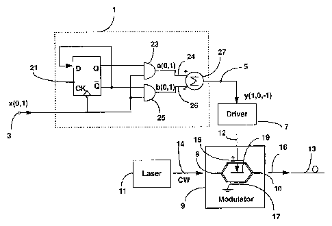
Figure 1 illustrates the blocks used to perform the duobinary
coding and modulation operations according to the invention. A
coding circuit 1 receives the binary input sequence x(0,1) at the input 3
CA 022~36l4 l998-ll-0~
W098/44635 10 PCT/CA98/00275
and provides the duobinary output sequence y(0,1,-1) at output 5. The
output sequence y(0,1,-1) is input to driver 7 which provides the
driving signal 12 on electrode 19 of modulator 9.
Modulator 9 illustrated in the embodiment of Figure 1 is a Mach-
Zehnder interferometer. A bias voltage Vgias is applied between
travelling wave electrodes 15 and 17. A laser 11 provides a CW optical
carrier signal 14 to the input port 8 of the optical wave-guide splitter of
modulator 9 in the known manner. A modulated optical signal 16 is
obtained at the output port 10 of the wave-guide combiner of the
modulator and coupled into optical fiber 13 for transmission.
Coding circuit 1 comprises a D-type flip-flop 21 connected with
the inverting output Q to the D input for obtaining a delay with a
period T, which is needed for simultaneously obtaining the bits xk and
xk 1. The binary stream x(0,1) is applied to the clock input of the flip-
flop 21. The state of this flip-flop after each bit Xk is equal to the input
(D) before the bit xk, or in other words xk=D. In this way, whenever the
input sequence x(0,1) comprises a succession of "O"s, a succession of
"1"s or a "0" bit followed by a "1", flip-flop 21 maintains its anterior
state, which could be logic "0", with Q=0, Q =1, or logic "1", with Q=1, Q
=0. Whenever a logic "1" xk bit is followed by a logic "0", flip-flop 21
changes its state. This is shown in rows 2 and 3 of Tables 2 and 3 below.
The binary stream x(0,1) is also applied to an input of a first AND
gate 23 and an input of a second AND gate 25. The second input of
AND gate 23 receives the output Q of flip-flop 21, such that a binary
sequence a(0,1) is obtained at the output of AND gate 23, where each bit
ak of sequence a is defined ak = xk + Xk_l. This is shown in row 4 of
Tables 2 and 3 below.
The second input of AND gate 25 receives output Q from flip-
flop 21, such that a binary sequence b(0,1) is obtained at the output of
AND gate 23, where each bit bk Of the sequence b is defined
bk = Xl, + Xk-l . This is illustrated in row 5 of Tables 1 and 2 below.
The output of both AND gates 23 and 25 is applied to a
summation circuit 27 to provide the coded stream y(0,1,-1) at output 5.
The summation circuit 27 effects an algebraic summation of the signals,
rather than the logic "AND" effected by gates 23 and 25.
Another advantageous implementation of the optical
modulation operation according to this invention is based on a M-Z
CA 022~3614 1998-11-0~
WO 98/44635 11 PCT/CA98/00275
modulator configuration that is driven differentially, as shown in
Figure lA. In this case, the driving signal is a differential signal
provided on lines 12 and 12', respectively, these being generated with a
differential pair of drivers 19 from duobinary sequence y(1,0,-1).
Travelling wave electrodes 15,17 receive each on a first end, close to
input 8, the active electrically modulated signal from the respective
line 12 or 12'. A first matching impedance Zl connects the second end
of electrode 15, close to the output port 10 of the modulator to ground,
while a second matching impedance Z2 connects the second end of
electrode 17 to ground.
In this way, the impedance of each travelling wave electrode is
substantially twice the impedance to ground of the individual active
lines, creating a virtual ground line. This virtual ground line is not
electrically connected to a physical ground, but is located somewhere
between the travelling wave drive electrode, substantially parallel to
the direction of propagation of the drive RF wave. The effect of using
this drive implementation is to reduce the drive amplitude required of
individual drive circuits to approximately half that required for the
push-pull drive configuration described earlier.
The following examples show how a binary input sequence is
transformed into the duobinary output sequence according to the
nventlon:
Table 2: Example 1 of coding a binary sequence xk, comprising an
even number of successive "1"s into a duobinary sequence Yk
Binary input xk 1 1 0 0 1 1 0 0 1 1 0 0
2 Q 0 0 1 1 l I 0 0 0 0 1 1
3 Q 1 1 0 0 0 0 1 1 1 1 0 0 0 o
4 ak-Xk AND Q o 0 0 0 1 1 0 0 0 0 0 0
bk=XkAND Q I I 0 0 0 0 0 0 1 1 0 0 0 O
6 Yk = ak +bk-l 1 1 0 0 -1 -1 0 0 1 1 0 0
CA 022~36l4 l998-ll-0~
WO 98/44635 12 PCT/CA98/00275
Table 3: Example 2 of coding of a binary sequence xk into a duobinary
sequence Yk
Binary input xk o 1 0 1 0 1 0 O 1 1 1 1 0 0
2 Q 0 0 1 1 0 0 1 1 1 1 1 1 0 0 0
3 Q 1 1 0 0 1 1 0 0 0 0 0 0
4 ak=Xk ANDQ o 0 0 1 0 0 0 0 1 1 1 1 0 0 0
bk=Xk AND Q o 1 0 0 0 1 0 0 0 0 0 0 0 0
6 Yk = ak +bk-l O 1 0 -1 0 1 0 0 -1 -1 -1 -1 0 0
Figure 2A illustrates an embodiment of the summation circuit
according to this invention, which receives bits ak and bk of the binary
sequence a(0,1) and b(0,1) and provides the bits Yk Of the output
sequence. Figure 2B shows the truth table for the circuit of Figure 2A.
As seen in the above Tables 2 and 3, the bits of the output sequence
y(0,1,-1) take a first value, defined as logic "1" when ak=0 and bk=1, a
second value, defined as logic "-1" when ak=1 and bk=0, and a third
value, defined as logic "0", when both ak=bk=0. It is to be noted that
ak=1, and bk=1 is not a valid input, as seen above in connection with
the description of the coding circuit.
The summation circuit comprises a first transistor 35 which
receives the bits of the first binary sequence a(0,1) on the base. The
collector of transistor 35 is connected to a load resistor (R), referred to
with numeral 41, and the emitter is connected to VDD through a
current source 39. A second transistor 33 receives on its base an
inverted version of the second binary sequence b(0,1), provided by
inverter 31. The collector of transistor 33 is also connected to the load
resistor 41 and the emitter to a second current source 37. Both current
sources 37 and 39 provide a current "i" through resistor R when the
respective transistor conducts.
A bit Yk obtained at output 5 can take three different values, iR,
2iR and 0 Yk takes the value i R when signals ak and bk are logic "0",
which corresponds to transistor 33 conducting and transistor 35 being
blocked. When ak=0 and bk=1, the signal bk becomes logic "0", and
transistors 33 and 35 are both conducting, so that the potential at output
5 takes the value 2i R. When ak=1 and bk=0, the signal bk becomes
logic "1" and both transistors are blocked, and Yk becomes 0. If the
CA 022~36l4 l998-ll-0~
WO 98/4463S 13 PCT/CA98/00275
summation circuit 27 is ac coupled, the three levels become: logic "1" is
i.R; logic "0" is 0; and logic "-1" is -i.R.
It is also to be noted that the adder illustrated in Figure 3 may
replace the driver module 7.
Figure 3 illustrates how the modulation is effected for a
duobinary sequence "1,0,0,0,-1,-1. The bias voltage Vgias is applied
between electrodes 15 and 17 and the duobinary coded driving sequence
is applied on electrode 19 of modulator 9, as shown in Figure 1. The
optical duobinary signal has two levels "on" and "off", the phase of the
"on" state alternatively taking values of "0" and "Jt". For the case
shown in Figure lA, VBias is the virtual ground voltage obtained as
discussed above.
Figure 4 shows in solid lines the variation of the spectral density
with frequency for an optical signal obtained with the duobinary
encoder of Figure 1. The dotted line illustrates the same parameter for
the duobinary scheme reported in [2], [3] and [4]. A pseudo-random bit
sequence (PRBS) was used for this comparison. As seen in Figure 4, the
dc component for the solid line curve obtained with the coding circuit
of the invention is lower than the dc component of the prior art
encoders.
While the invention has been described with reference to
particular example embodiments, further modifications and
improvements which will occur to those skilled in the art, may be
made within the purview of the appended claims, without departing
from the scope of the invention in its broader aspect.