Note: Descriptions are shown in the official language in which they were submitted.
CA 02253707 1998-10-23
WO 97/40937 PCT/US97/07269
1 -
TN SITU METHOD FOR METALIZING A SEMICONDUCTOR CATALYS'~'
The present invention relates to a method for
depositing a metal onto a semiconductor catalyst and, more
particularly, to the photodeposition of metal onto a
catalyst in situ on a reaction support surface for the
photopromoted degradation of contaminants in a fluid stream.
Chemical and biological agents from a variety of
sources present hazards to health and the environment,
particularly when they enter the air we breathe and the
water we drink. For this reason, there has long been a need
for efficient, cost effective methods for removing contam-
inants from fluid streams. In addition to the obvious
problems of water and soil remediation, indoor air pollution
has recently been identified as a health risk. In each of
these areas, the need for efficient solutions has become
increasingly acute with the advent of more stringent
2o regulatory standards.
Considerable effort has been expended in recent years
toward the development of methods and techniques for
removing destructive compounds and biological agents from
fluid streams. A particularly promising approach is the
photopromoted catalyzed degradation of such compounds and
agents, which involves the oxidation and/or reduction and
destruction of organic materials including bacteria, viruses
and pesticides, inorganic materials including carbon
monoxide, ammonia and hydrogen sulfide, and the removal of
odors including, e.g. garlic odor and onion order. Such
processes are disclosed in Lichtin et al., U.S. Patent Nos.
4,861,484 and 4,980,040, Matsunaga, U.S. Patent No.
4,788,038, Raupp et al., U.S. Patent No. 5,045,288, and Bard
et al., U.S. Patent Nos. 4,264,421 and 4,303,486. Specific
devices for these purposes are disclosed in Matthews et al.,
J. Phys. Chem. 1987, 91, 3328-3333; Robertson et al., U.S.
Patent Nos. 4,892,712, 4,966,759 and 5,032,241; and Anderson
CA 02253707 2001-O1-19
WO X7/40937 PCT/US97107269
2
et al., U.S. Patent No. 5,035,784.
Photopromoted catalytic degradation involves exposing a
i contaminated fluid stream to a catalyst in the presence of
air or oxygen and a light source which activates the
catalyst. The catalyst used is often an oxide of a
transition metal, sLCh as Ti02, but can also be any of a
variety of other known semiconductor catalysts.
In most prior applications, a catalyst is either kept
in a fluidized bed or coated onto the surface of a support
for contact with a contaminated fluid stream. One common
support surface is the smooth interior wall of: a reaction
vessel, which is typically made of glass. A more
sot:>histicated arrangement is disclosed in ,7acoby et al.,
U.S. Patent No. 5,449,443, in which a catalyst is affixed to
flexible strips exposed to a contaminated fluid stream. A
blower unit m«ves the Cluid through the flexit~le strips, anti
thus into contact with the catalyst. An ultraviolet light
2U source irradiates the strips to activate the catalyst and
oxidize contaminants in the fluid stream. Another approach,
disclosed in lJnited States Patent No. 4,888,101 to Cooper,
is to "entrap" the semiconductor, either within a layer of
glass wool confined between two transparent plates or within
pores on the surface of a solid support material.
As described in the Bard '421 patent, in many
circumstances the presence of a suitable metal on the
semiconductor catalyst increases the efficiency of the
degradation process. Noble metals, such as platinum and/or
3U pa:Lladium, are often used for this purpose; however,
existing methods for distributing and affixing the metal
tend to be wasteful of these costly materials.
More specifically, metal has heretofore been deposited
onto a semiconductor catalyst in powder form by illuminating
the powder in a suitable metalizing solution. The catalyst
then must be filtered and washed thoroughly before use,
however, before it is placed in a fluidized bed or other
CA 02253707 2001-O1-19
~rU !~71~t~)937 PCT/US97107269
3
reactor structure for use in degrading contaminants in a
fluid stream.
The filtering process is laborious and time-consuming,
especially for ultra-fine particle size semiconductor
catalysts like Degussa~P-25 titanic. If the catalyst is
subsequently affixed to a support structure, metal will be
present everywhere the catalyst is placed, regardless of
whether the catalyst at a given location will be exposed to
light in use. Much of the costly metal component is thus
l0 located where it cannot contribute to the degradation
process.
Accordingly, there is a pronounced need for more
efficient and more economic methods of metalizing
semiconductor catalysts for the photopromoted catalytic
degradation of compounds in a fluid stream.
SLUMMARY OF THE INVENTION
The present invention involves the photodeposition of a
suitable metal onto a semiconductor catalyst after the
catalyst is affixed to a reaction support surface. Because
the metal is deposited selectively where light impinges on
the semiconductor catalyst, the distribution of metal can be
pa~~tially controlled by controlling the distribution of
light in the deposition process. Thus, metal can be
det~osited selectively on a single face or side of a reaction
sut~port surface, such as a fibrous matte web of the type
used in many filtering applications. In one advantageous
embodiment, the deposition of metal takes place in the
actual photocatalytic reactor within which a particular
suE~port surface is to be used, or at least in a structure
having a similar geometry. This causes metal to be
det.~osited only where light impinges on the catalyst during
use, thereby minimizing waste and process inefficiency. The
resulting structure thus has metal deposited in a
sut~stantially uniform layer over the portions of the
catalyst receiving light, and catalyst can be absent at
CA 02253707 2001-O1-19
4
locations which do not receive light during the
photodeposition process.
The catalyst and the metal may be applied to the reaction
support surface together, as in the form of a slurry, or may
be applied separately. In either case, the two elements are
initially separate and the metal is deposited onto the
catalyst only with the incidence of light. Thus, the catalyst
undergoes metalization in situ on the catalyst support surface
itself.
Accordingly, the method of the present invention for
metalizing a semiconductor catalyst comprises the steps of:
providing a semiconductor catalyst on a reaction support
surface with a source of metal in proximity to the catalyst;
and illuminating at least a portion of the catalyst thereby
depositing the metal selectively on the illuminated portions
of the catalyst. In one aspect, the catalyst is illuminated
in the manner the catalyst is later to be illuminated in use.
More specifically, the illumination step may involve
placing the semiconductor catalyst in a reaction chamber or
other structure configured to illuminate the catalyst support
surface in the manner it will be illuminated during use in the
catalytic degradation of compounds in a fluid stream. The
catalyst and the source of metal can be introduced to the
reaction chamber together, as in the form of a single slurry,
or separately.
The invention also provides a structure for the
photocatalytic degradation of compounds in a fluid stream
comprising a reaction support surface at least partially
coated with a semiconductor catalyst affixed thereto, and
having a light-facing portion, and a metal deposited
selectively on said light-facing portion.
CA 02253707 2001-O1-19
4 (a)
BRIEF DESCRIPTION OF THE DRAWINGS
The above and other features of the present invention may
be more fully understood from the following detailed
description, taken together with the accompanying drawings,
wherein similar reference characters refer to similar elements
throughout and in which:
FIGURE 1 is a diagrammatic view of a catalyst-coated
reaction support surface under illumination to deposit metal
in sccorc3ance with the teachings of the r~resent invention.
CA 02253707 2001-O1-19
~1.~ 97/40937
PCTIUS97/07269
the thicknesses of the support surfaces and its coating
being exaggerated for purposes of illustration;
FIGURE 2 is an isometric view, partially broken away,
of a room air cleaner within which the metal deposition of
5 the invention can take place; and
FIGURE 3 is an isometric view, partially broken away,
showing a fluid reactor, such as a ground water remediation
reactor within which the metal deposition of the invention
Call take place. This reactor is useful, for example, in
practicing one superior method of removing and destroying
Volatile Organic Compounds (VOC's) in ground water.
According to this method, a ground water stream is passed
counter to an air stream (so called "air stripping") so that
the VOC's enter the air stream. The air stream is then
passed to a device like that illustrated in FIGURE ~ for
degradation of the VOC's.
DETAILS DESCRIPTION OF THE DRAWINGS
Referring now to the drawings, FIGURE 1 is a
diagrammatic representation of a reaction environment l0
constructed according to one embodiment of the present
invention. The reaction environment 10 contains a reaction
support surface 12, which in the illustrated embodiment is a
fibrous matte web supporting a semiconductor catalytic
coating 14 irradiated by a light source 16. A contaminated
fluid stream 1S, which may be either gaseous or liquid,
passes through the matte web 12 for reaction with the
catalytic coating under exposure to light from the source
16. The reaction mechanism is photopromoted catalytic
oxidation, which degrades chemical contaminants and destroys
biological agents. The catalytic coating 14 is at least
partially "metalized", i.e., coated with a suitable metal, to
improve the efficiency of the chemical reaction and protect
the catalyst.
CA 02253707 2001-O1-19
1V0 07/40937 PCTIUS97/07269
6
The matte web 12 may be a sheet-like body made up
of a large number of densely-packed fibers forming a porous
wet, which permits fluids to pass from one of its major
surfaces, or "sides", to another. The web may be formed by a
process similar to that used in the paper-making industry,
using fibers of any suitable material. A binder will also
l0 typically be used to hold the fibers together without
inhibiting the flow of fluids through the web.
The fibers of the matte web 12 may be made up of glass,
cellulose or a suitable synthetic polymer, such as
polyester, with glass being preferred in some circumstances.
In one advantageous embodiment, the matte web 12 is a
sut,stantially self-supporting sheet through which air or
other fluids can be passed in a lateral direction from a
first major surface 20 to a second major surface 22. The
semiconductor catalyst 14 is then distributed over the
length and width of the matte web, sometimes selectively in
the form of the coating illustrated in FIGURE 1. In other
cases, however, the catalyst is located on both major
surfaces of the web, or distributed throughout its
thickness. In each case, however, at least some of the
catalyst must be disposed to receive light from the light
so«rce 16.
~'he semiconductor catalyst is metalized, as stated
above, to enhance process efficiency and prevent
deterioration of the catalyst. The metal used may be a
3o not~le metal, such as platinum, palladium, etc., and is
affixed to the catalyst in situ after the catalyst is placed
on the matte web. This is accomplished by irradiating the
catalyst in the presence of a source of metal so that light
hits the catalyst in the same pattern and at the same
intensity as it does when the web is used in the degradation
process. While not bound by any theory, it is believed that
photons absorbed by the catalyst create charge carriers
CA 02253707 1998-10-23
WO 97140937 PCT/US97I07269
7
which interact with metal ions to bond the ions to the
catalyst, causing the metal to be deposited selectively
where light impinges. An advantageous manner of
accomplishing this is to place a matte web containing a
catalyst and a source of metal in the reactor within which
the web will ultimately be used. Metal deposition occurs
then automatically at the desired locations when the light
source is activated, with less deposition of metal in "dark"
areas.
l0 One method of preparing the matte or other reaction
support web 12 is to formulate a slurry containing the
catalyst and the source of metal in an aqueous solution.
Where the catalyst is titanium dioxide ("titania"), a useful
form is Degussa P-25 sold by the Degussa Corporation. The
slurry may then be composed, for example, of between five
and nine parts de-ionized water and one part Degussa P-25,
with between 0.01 and 0.10 percent of the metal source,
based on weight of the titanium dioxide. When the metal is
platinum, the source may be any suitable platinum-containing
compound, as .O1 M hexachloro-platinic acid in 0.1 M
hydrochloric acid, neutralized with sodium carbonate and
brought to a pH of about 4 by the addition of acetic acid.
The slurry is coated onto the second major surface 22 of the
matte web 12. Alternatively, the mixture may be coated onto
both surfaces (20 and 22) of the web, or distributed through
the thickness of the web. In the latter case, the slurry
can be incorporated into the matte web during formation,
either in an aqueous bath used to form the web (for "water
laid" webs) or on the fibers themselves, by for example,
spraying (for "air laid" webs). After the web containing the
semiconductor catalyst is prepared, it is inserted into the
reaction chamber and illuminated in exactly the way it will
be illuminated when used to degrade contaminants.
In an alternate form of the method, the slurry is
prepared by mixing de-ionized water with the same catalyst
without a source of metal ions. The slurry is then coated
or otherwise introduced into the matte web 12, after which a
CA 02253707 1998-10-23
WO 97/40937 PCT/US97/07269
8
source of metal ions is separately introduced to the web.
The source of metal ions may be the same as described above,
but sprayed directly onto the matte web. The carrier is
then exposed to illumination of appropriate wavelength,
which may be accomplished by insertion into the reactor, for
bonding of the metal to the catalyst in a distribution
corresponding to the pattern of illumination in use.
Referring now to FIGURE 2, an air cleaning apparatus
100 is one specific form of the reaction environment 10 of
FIGURE 1. The air cleaning apparatus 100 has a cylindrical
reaction support structure 102 surrounding four spaced-apart
light sources 116 parallel to its axis. The reaction
support structure 102 is itself contained within a generally
cylindrical housing 104, which defines a reaction chamber
having inlets 106 through its side walls and an outlet 108
at its lower end. A fan 109 within the housing 104 draws
air into the reaction chamber through the inlets 106 and the
reaction support structure 102, and expels the air through
the outlet 108. The reaction support structure 102 is
fabricated from a matte web 110 similar to the matte web 10
of FIGURE 1, but is pleated over its circumference to
increase the surface area over which the degradation
reaction takes place. The upper and lower ends of the
reaction support structure 102 preferably form an effective
seal against the interior housing 104 so that the fan 109
draws essentially all of its air inwardly through the
reaction support structure 102 and expels substantially all
of the air through the outlet 108. Of course, each of the
variations of the matte web and the disposition of catalyst
and metal described above with respect to the web 10, apply
to the web 110, as well.
Although the semiconductor catalyst (not specifically
shown) can be distributed throughout the web, if desired, it
is advantageous in many situations to coat only the interior
surface of the matte web 110 because it is only at that
location that the catalyst receives light from the light
sources 116. Even if the semiconductor catalyst and the
CA 02253707 1998-10-23
WO 97!40937 PCT/US97107269
9
source of metal ions are present elsewhere in the matte web
110, however, it is metalized only near its inner,
illuminated surface when the in situ method is used.
The air cleaning apparatus 100 operates particularly
well as a room air cleaner because any relatively large
contaminants are filtered out by the matte web at its outer
surface, and thereby separated from the activated portion of
the semiconductor catalyst. Thus, the illuminated portion
of the catalyst is not masked by such impurities, leaving it
free to react with the gaseous or very small particulate
contaminants that could not otherwise be removed from the
air stream. Thus, the matte web 110 acts advantageously to
mechanically filter large contaminants and chemically
degrade hazardous Volatile Organic Compounds (VOC's) and
other gaseous impurities. When glass fiber matte of the
type used in HEPA filters is used, particles as small as
approximately 0.3 microns in diameter are effectively
removed by filtration.
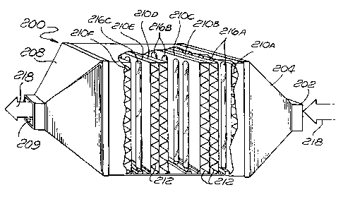
Turning now to FIGURE 3, an apparatus 200 is designed
to remove contaminants from either gaseous or liquid streams
containing concentrations of contaminants large enough that
more than one "pass" through a catalyst support structure is
required. The apparatus 200 has a fluid inlet 202 leading
to a transition element 204 and ultimately to a principal
reaction chamber 206, after which the stream is funneled
down again by a transition element 208 to exit through a
fluid outlet 209. Within the principal reaction chamber 206
are a plurality of reaction support structures, 210A, 210B,
210C, 210D, 210E and 210F. Each is pleated in the manner of
the support structure 102 of FIGURE 2, but arranged to form
a substantially flat structure through which fluid passes in
a transverse direction. These flat support structures are
individually replaceable and are made up of a matte web
material 212 which is the same as the webs 12 and 112 of
FIGS. 1 and 2, respectively. When the apparatus 200 is used
to clean a gaseous stream produced in the course of
groundwater remediation, the reaction support structures
CA 02253707 2001-O1-19
210A-27OF may be pleated filters approximately 6lcm (two feet) square and
between 2.54 and 5.08cm (one and two inches) thick. Such filters in tire
il:lustlatf:d arrangement are suitable for degrading a relatively large
proportion of the contaminants in stream at flow rates of between 85 and
850m 3/5 (50 and 500 cubic feet per minute).
A plurality of coplanar light sources 216A are disposed
between and parallel to the reaction support structures 2loA
arrd 2loB, a similar series of coplanar light sources 216B
are disposed between the reaction support structures 210C
l0 .rnd 2loD, and yet another series of light sources 216C are
disposed between the reaction support structures 110E and
a'lOF. The upper pleated surfaces of reaction support
~~tructures 210A, 210C and 210E, and the lower-pleated
_;urfaces of the reaction support structures 210E3, 210D and
1~ O10F, are coat.<ed with semiconductor catalyst (not
specifically shown) similar to the semiconductor catalytic
coating 14 of FTGURE 1, and are metalized in the manner
described above in connection with the embodiments of
FIGURES 1 and 2.
A fluid stream 21f3 entering the fluid inlet 20F3 is
filtered by tire matte web 212 of the reaction support
structure 210A, mechanically removing the relatively large
contaminants from the fluid stream. Contaminants too small
for removal by the matte web 212 pass through the reaction
support struct_r.rres and contact tire catalytic coatings
thereon. Because the surfaces containing the metalized
catalyst are illuminated by the light sources 216A, 2168 and
216C, chemical and biological contaminants are effectively
degraded within the principal reaction chamber 206. By the
time the flui~t exits the upper reaction support structure
210D, the level of contaminants is significantly reduced.
If the variou:~ elements of the apparatus 20o are designed
properly, the fluid leaving through the fluid outlet 209 has
an average contaminant concentration well within acceptable
environmental and health limits.
In each of the illustrated embodiments, the parameters
of the light sources, the matte webs, the catalytic coatings
... "~~r, ~ucGT
CA 02253707 1998-10-23
WO 97/40937 PCT/US97/07269
11 -
and the metalized coatings are calculated to cause the
semiconductor catalyst to be illuminated within a
preselected range of optimal values appropriate for the
chemical processes being performed. Contaminants are
degraded through an oxidation process which requires the
presence of oxygen or other suitable oxidizing agent. The
oxygen content of air is usually sufficient for the reaction
to proceed efficiently; however, oxygen may be added if
desired.
For a light source of a given intensity, the amount of
light reaching a particular portion of the semiconductor
catalyst on the matte webs 12, 112 and 212, depends on both
the inclination angle of the surface of the matte web
relative to the incoming light and the distance of the matte
web from the light source. The optical characteristics of
the reaction chamber, and thus the efficiency of the
photopromoted catalytic reaction, are controlled by
selecting appropriate dimensions and shapes for the
components involved. As a general rule, an increase in
catalyst surface area lowers the average light intensity on
the catalyst itself. In the embodiments of FIGURES 2 and 3,
multiple lamps are utilized within the reaction chamber to
ensure that a sufficient number of photons are absorbed.
Light sources within the reactors of FIGURES 1-3
comprise at least one ultraviolet lamp capable of emitting
light within the wavelength range of 175 to 500 nanometers
(nm). In the illustrated embodiments, the light source is
preferably one or more General Electric F40/BL lamps, which
are 40 watt bulbs emitting radiation having a wavelength of
approximately 360 nm, or Philips PLS 9W/10 lamps or Sylvania
FC8T9/350/BL/RS lamps. Any other lamp or bulb emitting
light capable of being absorbed by the catalyst can be used
for this purpose, as well, including both medium and high
pressure mercury vapor lamps and fluorescent lamps.
Because the deposition of metal according to the
invention and the subsequent process of chemical degradation
are accomplished with the same catalyst, similar light
CA 02253707 2001-O1-19
WO 97/40937 PCT/US97107269
12
sources can and should be used for them. The shape of the
reaction support and the geometry of the reaction chamber
can vary significantly from one embodiment to the other,
however. For example, the method and structure of the
present invention are useful in the context of each of the
embodiments of FIGURES 1-3, as long as the metal is
deposited under the same or similar illumination conditions
as the ultimate degradation process. The teachings are also
applicable to any other reactor for the photocatalyzed
degradation of compounds in a fluid stream. In each case,
the metal is~deposited onto the catalyst in situ on the
reaction support surface, often in the very reactor to be used
in the degradation process. This results in substantial
process and efficiency advantages over the prior art in which
the semiconductor is coated with metal before it is placed on
the reaction support.
The semiconductor catalyst of the present invention can
be any of a variety of suitable semiconductor materials, but
25 is preferably an oxide. One advantageous catalyst is
titanium dioxide; however, other suitable catalysts, such as
ZnO, WO., or their mixtures, can also be used. As noted
above, the activity and selectivity of the catalyst can be
improved by depositing noble metals (platinum, palladium,
30 etc.) onto the catalyst by one of the methods described
above.
In one advantageous embodiment, the catalyst can be
introduced and the metal can be deposited in the process of
forming the reaction support surface. This is particularly
35 promising where the reaction support is a fibrous matte web
made of glass, cellulose or other suitable fibers. The
fabrication is then quite similar to a papermaking process
CA 02253707 2001-O1-19
13
or a process for making a filter media, and can be of either
the water-laid or air-laid variety. The semiconductor
catalyst, which can be titanium dioxide of the photoactive
type, is then typically added to a slurry or other mixture
from which the support is to be made. This causes the
catalyst to be distributed throughout the thickness of the
support. A suitable metal-containing substance is either
added to the mixture or sprayed onto the support, after
which the support is exposed to light of appropriate
wavelength on one or both sides. This causes the metal to
be deposited selectively onto the illuminated portions of
the catalyst, where it increases the efficiency of the
degradation reaction and protects the catalyst. Thus, the
use of the metal is extremely efficient and t:t~ere is no need
to filter out catalyst particles for subsequent attachment
to a reaction support surface.
In order that the invention be more clearly understood,
the efficiency of the metalized catalyst of the present
invention is further demonstrated by the fol~.owing examples,
which should not be construed to limit the scope of the
invention. Each example compares the results achieved by
passing an air stream containing a particular contaminant
through a tubular reactor with an illuminated surface coated
with non-metalized titanic, as compared with a similar
reactor coated with titanic metalized in accordance with the
teachings of the present invention. Each photocatalytic
reactor is a Pyrex shell (52 millimeter inside diameter by
1200 millimeters length) having a catalytic coating on its
inner wall and an axially-directed lamp surrounded by a
protective Pyrex liner (45 millimeter outside diameter by
1200 millimeter length). The annular space between the
shell and the liner, which is the volume of the reactor, is
590 milliliters. The reactions were conduced with a host
air stream of high purity dry air from wesco (Grade Z.0).
All reactions were carried out at a pressure of 10.27 x 10⁴ Pa
(770 torr), and the reacted gases were analyzed by gas
chromatography after exposure to the catalyst and the light
f or the _
CA 02253707 1998-10-23
WO 97/40937 PCT/US97/07269
14
indicated periods. The semiconductor catalyst used in the
examples was P-25 titanium dioxide obtained from the Degussa
Corporation and prepared in a slurry of the type described
above in relation to the matte web of FIGURE 1, including
the metalized ion source described there. Metalization was
accomplished by the in situ method described herein.
Table 1 compares the rate of removal of 2045 parts per
million (ppm) of methanol from an air stream by passing it
through tubular reactor structures with and without
metalization of the titania catalyst. In the metalized
case, metal and catalyst are supplied together from a slurry
having a concentration of 0.05 percent metal by weight,
based on the titania. As shown in Table 1, the rate of
achieving ninety percent removal of methanol in this example
is much greater for the metalized titania catalyst.
Table 1
Reaction Time % R emoval
W,/ o meta 1 W,/ meta
1
0 0 0
1 8
2 19
3 29 40
4 34
6 40 65
10 60
12.5 71 96
18 88 100
25 99 100
CA 02253707 1998-10-23
WO 97/40937 PCT/US97/07269
Table 2 compares the rate of removal of 3500 ppm of
hydrogen from an air stream by passing it through the
5 illuminated reaction tubes of Example 1. The rate of
removal is significantly better for the metalized catalyst
case.
Table 2
Reaction Time % Removal
W / o Meta 1 W~/ Meta 1
0 0 0
40 lg
135 18 45
Example 3
Table 3 compares the rate of removal of 60 ppm of
hydrogen from an air stream by passing it through the two
illuminated reactors of Example 1. The rate of removal is
superior for the metalized catalyst case.
Table 3
Reaction Time o Removal
W,/ o Meta 1 W,/ Meta
1
0 0 0
1.7 20 50
3.5 32 70
5 50 73
6.5 72 100
10 100 100
13.5 100 100
CA 02253707 1998-10-23
WO 97140937 PCT/US97/07269
16
~xammle 4
Table 4 compares the rate of removal of 1000 ppm of
hydrogen from an air stream by passing it through the
reaction tubes of Example 1. The rate of removal is
superior for the metalized catalyst case.
Table 4
Reaction Time o Removal
W~o Metal W/ Metal
0 0 0
1.5 32 39
3 47 69
6 78 98
10 100
Example 5
Table 5 compares the rate of removal of 12 ppm of
benzene by passing it through the metalized reaction tube of
Example 1, for two different moisture levels. The first
column shows the results with 0.8 percent moisture present
and the second column shows the results with 2.8 percent
moisture present. At the lower level of moisture, a yellow
discoloration built up within the tube, indicating byproduct
formation of the type encountered with nonmetalized titania.
Discoloration was not present at the higher moisture
content, which also removed benzene at a superior rate.
Table 5
Reaction Time % Removal
W/ Metal W/ Metal
(0 8% water)(2 88% water)
0 0 0
CA 02253707 1998-10-23
WO 97/40937 PCT/US97/07269
17
3 31
7 41 87
11 67 100
13 83 100
20 100 100
Exam In a 6
Table 6 compares the rate of removal of 10 ppm of
carbon monoxide from an air stream by passing it through the
tubular reactors of Example 1. The rate of removal for the
metalized catalyst is orders of magnitude greater than for
the nonmetalized catalyst.
Table 6
Reaction Time % Removal
W,/o Metal W/ Metal
0 0 0
20 10 100
56 20 100
406 60 100
Example 7
Table 7 compares the rates of removal of 35 ppm of
carbon monoxide from an air stream by passing it through a
tube with an illuminated surface coated with metalized
titania according to the method of the present invention.
The results shown are for three different metal
concentrations, specifically, 0.01 percent, 0.05 percent and
0.10 percent platinum. All three of these values are
percentages of platinum in the slurry, calculated by weight
based on the titania present. Although the highest rate for
this particular example was obtained with 0.05 percent
CA 02253707 1998-10-23
WO 97/40937 PCT/US97/07269
18
platinum by weight, all of the metalized samples gave rates
for greater than the nonmetalized titania data of Example 6.
Table 7
Reaction Time % Removal
0 O1% Metal 0 loo Metal0.05% Metal
0 0 0 0
4 41 58 71
7 70 81 95
10 85 96 100
100 100 100
15 From the above, it can be seen that the ~n situ
metalization method of the present invention provides a
significant increase in efficiency over nonmetalized
catalysts without the processing complexity encountered with
prior art metalization methods.
The appended claims are not limited to the embodiments
described herein, but rather are intended to cover all
variations and adaptations falling within the true scope and
spirit of the present invention.