Note: Descriptions are shown in the official language in which they were submitted.
CA 022~4310 1998-11-16
METHOD OF SELECTING BETWEEN MULTIPLE CLOCK DRIVE
SOURCES FOR A BACKPLANE CLOCK SIGNAL
FIELD OF THE INVENTION
This invention relates in general to shared bus systems and more specifically to a
system of backplane clock signal drivers installed in circuit cards connected to the
backplane of a shared bus system wherein the switching of the drivers does not cause
any interruptions in operation of the circuit cards.
BACKGROUND OF THE INVENTION
It is well known in the art of shared bus systems, such as the Mitel~ Open Telephony
Platform System, that a backplane clock signal may be driven by any circuit card15 installed in the backplane of the system. In most cases, more than one installed card
may be capable of driving the clock signal. Moreover, it may be necessary to transfer
control of the backplane clock signal from a first card to a second card while the
shared bus system is operational. This necessila~es an interruption-free handover of
control of the clock signal from the first card driving the clock signal to the second
20 card.
SUMMARY OF THE INVENTION
The invention allows for switching from a first card driving the backplane clock2s signal to a second card driving the backplane clock signal without causing a
disturbance, or interruption, to the signal, thus allowing such switching to be done
while the shared bus system is operational and with no adverse effects.
The switching is controlled by a controlling card within the system which bro~(lc~t~ a
30 message onto the backplane via backplane mess~ging signals. The message is
addressed to the above-mentioned second card (i.e. the card which is expected to drive
the backplane clock signal). The card which is currently driving the bus is also
CA 022~4310 1998-11-16
notified of this message. In a synchronized manner, the driving card, the above-mentioned first card, deasserts its enable signal and the addressed card, the above-
mentioned second card, asserts its enable signal thus taking over the function of
driving the backplane clock signal.
s
BRIEF DESCRIPTION OF THE DRAWINGS
An embodiment of the invention is described below with reference to the
accompanying drawings, in which:
Figure 1 is a diagram of a shared bus system;
Figure 2 shows a system of backplane clock signal drivers in accordance with thepresent invention for driving clock signals on the shared bus system of Figure l;
Figures 3A, 3B are schem~tic diagrams which, in conjunction with one another, show
cil~;uill y for implementing the system according to the plerelled embodiment; and
Figure 3C is a timing diagram showing signals produced during operation of the
20 preferred embodiment of the present invention.
DETAILED DESCRIPTION OF THE PREFERRED EMBODIMENT
In the preferred embodiment, a serial, high-level data link control (HDLC) based
25 mess~ging system is implemented in a shared bus architecture, such as the MITEL'~'
Open Telephony Platform System. It should be noted that the inventive principlesapply equally to a parallel bus m~s~ging system. It should be further noted that such
a parallel bus based system is a variation upon the system set forth herein.
30 Turning to Figure 1, a shared bus system is shown co"l~ ing three circuit cards 10,
12, and 14. Each card 10, 12 and 14 has an individual clock source 16 which is
connected to a backplane clock signal 18 via individual tri-state drivers 20. Each tri-
CA 022~4310 1998-11-16
state driver 20 contains an enable signal 22 which, when asserted, causes the driver 20
to drive the backplane clock signal 18 using its clock source 16. Thus if card 10 is
driving the backplane signal 18, the driver 20 corresponding to card 10 is enabled and
the drivers 20 corresponding to cards 12 and 14 are disabled.
s
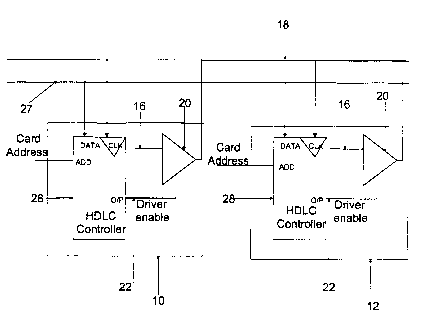
Turning to Figure 2, an Open Telephony Platform System, which is the preferred
operating environment of the present invention, is shown. Although only two cards
10 and 12 are shown in the figure, in a normal bus system many more cards, similar to
10 and 12, are present. In the Open Telephony Platform System, control messages are
0 transmitted to cards 10 and 12 via a pre~letermined 64 kB/s channel 27 located on the
backplane. The control messages are used to inform the cards 10 and 12 of a change
in backplane clock control. The control messages are sent via HDLC protocol with a
unique address for identifying the card 10 or 12 which is to take over control of the
backplane clock signal 18. Unique addresses are assigned to each card 10 and 12 to
act as identifiers for the control message so that the control message is delivered
correctly. A separate HDLC control block 28 is included in each card 10 and 12 for
selecting and decoding the control messages passed through the channel 27. Only the
card 10 or 12, whose address m~tl~h~s the address located in the HDLC message
address section, decodes, interprets and executes the control message while the other
20 cards simply decode the control message. The control message consists of a
Clock_Drive_Switch command which informs the above-mentioned first and second
cards of the upcoming change of control of the backplane clock signal 18. Depending
on the individual card 10 or 12, the Clock_Drive_Switch command causes differentactions. For instance, if the address located in the HDLC control message address
25 section is the unique address of card 10 and is not the unique address of card 12, the
driver 20 corresponding to card 12 is disabled and the driver 20 corresponding to card
10 is enabled.
Turning to Figures 3A,3B and 3C, details are shown of a circuit for transferring the
30 clock driving function from a first card 10 to a second card 12 along with a timing
diagram showing signals produced during the transferring of the clock driving
function.
CA 022~4310 1998-11-16
In the prerel,ed embodiment, the address located in the HDLC control message
address section is assumed to be the unique address of card 12.
s Backplane control message signals, transmitted by the channel 27, and the backplane
clock signal 18 are sent to the HDLC control block 28 located on each card 10 or 12
via input buffers 30 and 31 respectively. The HDLC control block 28, which is driven
by the backplane clock signal 18, produces two pulsed signals 32 and 34. The first
signal 32 is an address decode signal. The second signal 34 represents the
o Clock_Drive_Switch command and is generated from the decoding of the control
message.
The signal 32 of the addressed card 12 is an Address_Matched signal (shown in
Figure 3C) while the signal 32 of the unaddressed card 10 is an Address_Unmatched
signal (shown in Figure 3C). A mux 40 and a flip-flop 41, located on the cards 10
and 12, latches the signal 32 and produces an output signal labeled
Drive_Clock_Comm~n~1 This output signal is fed back into the mux 40 as well as
into a series of flip-flops 50 discussed herein below. The output
Drive_Clock_Command signals for the addressed card 12 and the unaddressed card
20 10 are shown in Figure 3C and labeled as Drive_Clock_Command (Card 12) and
Drive_Clock_Command (Card 10) respectively.
Reference line 46 in Figure 3C indicates the end of control of the backplane clock
signal 18 for card 10 and shows that the backplane signal 18 has no phase relationship
2s to the intern~l clock source 16 of the addressed card 12 prior to the outputting of the
Drive_Clock_Command (Card 12) signal.
Reference line 48 in Figure 3C indicates the beginning of control of the backplane
clock signal 18 for the addressed card 12 and shows that a phase relationship exists
30 between the backplane clock signal 18 and the internal clock source 16 of theaddressed card 12 after oull~ullillg the Drive_Clock_Command (Card 12) signal.
CA 022~4310 1998-11-16
s
In order to synchronize the Drive_Clock_Command (Card 12) and
Drive_Clock_Command (Card 10) signals to the internal clocks 16 of the addressedcard 12 and unaddressed card 10 l~e~ ely, flip-flops 50 must be used. The signaloutput from the flip-flops 50 (labeled as Enable_Clock_Drive in Figure 3B) for the
addressed card 12 and the unaddressed card 10 are shown in Figure 3C as
Enable_Clock_Drive (Card 12) and Enable_Clock Drive (Card 10) respectively.
When the Enable_Clock_Drive (Card 10) signal is deasserted for card 10, the
backplane clock signal 18 changes to a logic high through the action of an OR gate 56
0 and a Driver_Enable signal is deasserted through the action of an AND gate 60. The
Driver_Enable signal for card 10 is shown in Figure 3C and labeled as Driver_Enable
(Card 10). The deassertion ofthe Enable_Clock_Drive (Card 10) signal also results in
the backplane clock signal 18 being driven to a high state and causes the driver 20
corresponding to card 10 to operate in a high impedance mode. Subsequently, card 10
ceases to drive the backplane clock signal 18. A pull-up resistor 66 is also provided to
pull up the backplane clock signal 18 to a voltage high.
Flip flops 62 supply a delay (a ~ lll of three clock delays is necessary for thepreferred embodiment) between the termination of the control of the backplane clock
18 by card 10 to enabling of control of the backplane clock 18 by card 12. The OR
gate 56 and the AND gate 60 ensures that this occurs by asserting and deasserting the
drivers 20. The combination of the OR gate 56 and the AND gate 60 provide the most
basic logic function. Provided that the logic function is the same, any combination of
logic gates may be substituted for the OR gate 56 and the AND gate 60.
After the Driver_Enable signal for card 12 (shown as Driver_Enable_12 in Figure 3C)
is asserted, the tri-state buffer driver 20 corresponding to card 12 commences driving
the backplane clock signal 18. Simultaneously, the internal clock source 16 of card 12
is in a high clock phase and the backplane signal 18 is not driven low until the first
low phase at reference line 48 of Figure 3C.
CA 022~4310 1998-11-16
Operation of all flip flops 62 ensures that the backplane clock 18 runs interruption free
due to the time delay created by the flip flops 62. When control of the backplane
clock signal 18 switches, the backplane clock signal 18 goes through an extended high
clock phase between reference lines 46 and 48 (in the timing diagram of Figure 3C)
s but which does not disturb any phase locked loops or synchronous circuits being
driven by the backplane clock signal 18.
The backplane clock signal 18 and the internal clock source 16 for the addressed card
12 are shown in Figure 3C as a reference for the other signals.
It will be appreciated that, although only one embodiment of the invention has been
described and illustrated in detail, various changes and modification may be made.
One such modification relates to the selection of the driver 20. In the preferred
embodiment of the present invention, a tri-state buffer driver is disclosed but may be
s replaced by an open-collector or open-drain technology driver. The difference in
implementation involves the addition of a NAND gate (prior to the driver 20) with the
source clock signal 16 and the enable signal 22 as inputs to the NAND gate. Another
modification is that although a serial, HDLC based mess~ging system has been
described in the preferred embodiment, the same system may be applied to a parallel
20 bus mess~ging system. A third modification is that the messages need not be HDLC
encoded but can be unencoded. A fourth possible modification is that a differentnumber of delays may be inserted between the reference lines 46 and 48 of Figure3C. Also, the logic function produced by the OR gate 56 and the AND gate 60 may
be substituted for any other logic types as long as the function does not change. A
2s final modification is in the addressed control message command which is decoded by
all the cards. The command may be a broadcast command with the address of the new
driver incorporated as a field within the comm~n~. All such changes and
modifications may be made without departing from the sphere and scope of the
invention as defined by the claims appended herein.