Note: Descriptions are shown in the official language in which they were submitted.
CA 02254426 1998-11-20
DEVICE AND METHOD FOR DETECTING AND MEASURING FIBER PROPERTIES
Field of the Invention
This invention relates to a device and method for detecting and measuring the
physical properties of fibers. In particular, this invention relates to a
device and method for
detecting and measuring fiber properties, such as denier, eveness, percent
finish-on-yarn and the
presence, distribution and physical properties of interlacing nodes of man-
made and natural and
both continuous and staple, fibers, substantially in real-time.
Background of the Invention
In textile production, synthetic or man-made fibers are typically formed from
a
molten polymer material in a "spin-draw" process. The molten polymer, commonly
nylon or
polyester, is spun into filaments, five to five hundred of which are twined
together to form a
single fiber. The spun fiber is then drawn, altering the fiber's elasticity
and tensile strength, and
producing a continuous fiber with a desired final diameter. Natural fibers are
typically spun from
short lengths of natural material, such as wool or cotton, to form a staple
fiber.
During the processing of the fiber, a "finish", typically a liquid emulsion,
is
applied to the fiber to lubricate its filaments and reduce static electricity
buildup generated by the
flow of the fiber through the processing machinery. Generally, the finish is
water-based for
nylons and oil-based for polyesters.
The industrial production of polymer fiber generally occurs at rates of 2,000
to
8,000 meters per minute, and can be as high as 6,000 meters per minute.
Uniformity of the
physical properties of the resulting fiber is critical to the performance and
processing by the
destined end user. Lack of fiber uniformity can result in costly production
line shutdown, and/or
product irregularities for end users, such as entanglement or breakage of the
fiber during a
weaving process and inconsistent fiber coloration.
-1-
CA 02254426 1998-11-20
During fiber production, several variables, such as temperature, roll surface,
drawing speed, processing parameters and uneven application of the finish can
affect the
uniformity and properties of the fibers. Conventional measures of a fiber's
properties are denier,
the fiber density expressed as the weight in grams of a 9,000 meter length of
fiber; and percent
finish-on-yarn ("%FOY"), a measure of the amount of finish on the fiber; and
interlacing.
Interlacing nodes, also known as entanglement, are added to the fibers to
provide a bond between
the individual filaments that constitute each fiber. Generally, interlacing
nodes are created
regularly along the length of a fiber, typically every 5 - 20 cm, by exposing
the fiber to a high
velocity stream of air. Other fiber properties that are commonly measured
include evenness, a
measure of the variation of a fiber's denier, node distribution along the
length of a fiber, and the
size and formation of the nodes.
Currently, there is no reliable and cost-effective way to monitor the
properties of
fibers during production in real time as the fiber is being produced. As a
result, fiber properties
are measured after production. If the fiber properties fall outside accepted
tolerances, substantial
portions, or even whole runs, of production can be lost.
It is therefore preferable to determine fiber properties substantially in real-
time as
the fiber is being produced. Such a real time measurement system should be
able to withstand
shock, vibration, electromagnetic interference from equipment within a textile
plant, and
electrostatic charge build-up from contact with the passing fiber. The system
should be generally
insensitive to exposure to solvents used to clean the production line
equipment, and splattering by
finish as it is applied to the fiber.
In addition, if a real-time measurement system is to be adaptable to a variety
of
production environments, it should operate on a variety of fiber types.
Further, as a fiber is
composed of multiple filaments which can have different cross-sectional
geometries, such as
round, hollow, triangular and multi-lobed, the measurement system should also
operate with a
wide variety of fiber cross-sections.
Devices and analytical techniques exist for non-intrusive investigation of
materials
to deduce their physical properties. For example, dielectric sensors can
measure the effects that
-2-
CA 02254426 2006-01-19
the investigated material has on the capacitance of an imposed field. However,
as is well
known, such sensors exhibit problems with air gaps (United States Patent No.
5,045,795,
Hendrick and United States Patent No. 5,095,278, Hendrick). Air gaps severely
limit the
sensors' ability to measure dielectric properties of a sample material as air
and a vacuum
have the lowest theoretically possible permittivity,
United States Patent No. 4,706,014 to Fabbri and United States Patent No.
5,394,096 to
Meyer employ capacitive sensors to measure the diameter of a polymer fiber and
denier,
respectively. However, capacitive techniques can detect only relatively large
variations in
denier, can show extreme sensitivity to finish, and can be highly susceptible
to iYbar
orientation and cross-section. Thus, such systems are not generally usefnl.
Electrostatic sensors are also known but also suffer from disadvantages in
that they do
not exhibit good sensitivity, are strongly affeeted by humidity and must be
tnsintained at
a specific distance from the material under investigation.
United States Patent No. 5,394,340, which is owned by the assignee of the
present
invention, discloses a dielectric and capacitive sensor system for
identif'ying and
measuring substances, such as ice, on an aircraft wing. In this semor system,
sensor
electrodes are driven to produce an electric field in a pattern which
approximates a Bessel
function. Current measurements are then taken &om predetermined electrodes and
analyzed to determine the nature and thickness of a layer of material
overlying the sensor.
While tltis sensor system is appropriate for identifyinp, the presence or
absence of layered
materials on a surface, it is not capable ofineasuring the physical properties
of a material
moving at high speeds past the sensor.
Summary of the Tnvention
It is an object of the present invention to provide a novel deviee and method
for
detecting and quantifying the physical properties of fibers and like materials
substantially
in real time which obviates or mitigates at least some of the disadvantages of
the prior art.
-3-
CA 02254426 1998-11-20
In a first aspect of the present invention, there is provided a device for
measuring
at least one physical property of a fiber substantially in real time,
comprising:
a driven electrode for placement adjacent a fiber of which at least one
physical property is
to be determined, said fiber moving relative to said driven electrode;
a control means to apply a voltage to said driven electrode means to induce a
current in
said driven electrode means, said induced current varying according to said at
least one physical
property;
a sensing means for sensing said induced current;
amplitude and phase detection means responsive to said sensing means for
determining
amplitude and phase of said sensed current at predetermined intervals;
analyzing means for analyzing said amplitude and phase to determine a measured
value of
said at least one physical property;
output means for outputting information representing said measured value.
In another aspect of the present invention, there is provided a method for
detecting
and quantifying at least one physical property of a fiber substantially in
real time, said fiber
moving relative to a driven electrode means, comprising the steps of:
(i) applying a voltage to said driven electrode means for inducing a current
in said
driven electrode means, said induced current varying according to said at
least one physical
property;
(ii) sensing said induced current;
(iii) determining amplitude and phase of said sensed current;
(iv) analyzing said amplitude and phase to determine a value for said at least
one
physical property; and
(v) providing an output representing said value.
Brief Description of the Drawings
Preferred embodiments of the present invention will now be described, by way
of
example only, with reference to the attached Figures, in which:
Fig. 1 shows a block diagram of a device for detecting and quantifying in
accordance with the present invention;
-4-
CA 02254426 2006-01-19
FIG. la shows a block diagram of the detection unit of the device of FIG. 1;
FIG. 2 shows a top view of a sensor system of the present invention;
FIG. 3 shows a top view of a sensor unit of the present invention;
FIG. 4 shows a side view of the sensor unit of FIG. 3;
FIG. 5 shows a top view of a sensor head of the present invention;
FIG. 6 shows a side view of the sensor head of FIG. 5;
FIG. 7 shows a graphical representation of denier sensitivity for a device in
accordance
with an embodiment of the present invention;
FIG. 8 shows a graphical representation of pereent ITinish-ott-yam sensitivity
for a device
in accordance with an embodiment of the present invention;
FIG. 9 shows a graphical representation of magnitude response in accordance
with a
further embodiment of the present invention; and
FIG. 10 shows a block representation of the measurement and calibration
circuitry of an
embodiment of the pressent invention.
DETAILED DESCIiI[PTfON
A device 10 in accordance with att embodiment of the present invention is
sehematically
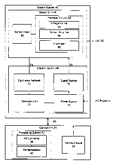
illustrated in FIG. 1. Device 10 generally comprises a sensor system 20
connected to a
control unit 24 through a communications system 28. Control unit 24 comprises
a
processing system 32 to acquire, convert and analyze data from the sensor
system 20 and
control circuitry 34 to control the operation of sensor system 20. Proeessing
system 32
includes an A/.D converter 36 and a microprocossor 40, such as an INTEL (trade-
mark)
80486, or better, and has a monitor for displaying results obtained with the
device and
other infomLation.
Sensor system 20 consists of a sensor unit 44 and an electronics unit 48.
Eleetronics unit
48 supplies excitation and control signals 52 to, and receives measurement
signals 56
from, sensor unit 44. Sensor unit 44 includes a sensor bead 58 and associated
inte=rfa.ce
circuitry 62, iiicluding voltage driven 64, a sense amplifier 66 and
thermistor 68, which
are responsive to the excitation and control signals 52 from electranics unit
48.
-5-
CA 02254426 1998-11-20
Electronics unit 48 generally comprises a calibration network 70, a detection
unit
72, a signal source 74, and power supply 76. In a presently preferred
embodiment, signal source
74 supplies a high frequency signal to drive sensor unit 44. As will be
apparent to those of skill
in the art, the optimal choice of this frequency depends upon the fiber and
finish being measured.
For example for common polymer fibers, the frequency will be in the range of
from about 100
kHz to about 1 MHz, although frequencies outside this range may be employed
for some
materials.
Fig. 1a shows an embodiment of electronics unit 48 in greater detail. In the
illustrated embodiment, detection unit 72 includes a magnitude detector 78 and
a phase detector
80, which receive signal 56 from calibration network 70, detect the magnitude
and phase of the
signal 56, respectively. A phase signal 81, representing the detected phase of
signal 56 is the
output of phase detector 80. Similarly, a magnitude signal 82, representing
the detected
magnitude of signal 56 is outputted from magnitude detector 78. Magnitude
signal 82 is
subsequently fed to a node presence detector 84 which detects the presence of
interlacing nodes
and outputs a presence signa185 indicating the presence of a node, as will be
more fully
described below. Phase signal 81, magnitude signal 82, and presence signal 85,
are then
transmitted to processing system 32. Phase signal 81 passes to processing
system 32 via a peak
detector 83 and filter 88. Similarly, magnitude signal 82 passes to processing
system 32 via a
peak detector 89 and a filter 90. Presence signal 85 is transmitted to
processing system 32 via a
pulse shaper 86. Generally, the output from pulse shaper 86, and filters 88
and 90 represent the
node position, phase and magnitude measurements of sensor system 20. A signal
(not shown)
from thermistor 68 can also be fed directly from the sensor unit 44 to the
processing unit 32. In
addition, general circuitry for filtering, scaling, amplifying and offsetting
measurement signals 56
can also be integrated into detection unit 72. In a presently preferred
embodiment, detection unit
72 operates upon analog signals 56, however, it is fully within the
contemplation of the inventors
that signals 56 can be digitized prior to input to electronics unit 48 and
such prior digitization
will not affect the general operation of device 10.
The design and construction of suitable electric circuits for interface
circuitry 62
and electronics unit 48 is not particularly limited and can be any suitable
configuration, as will
occur to those of skill in the art.
-6-
CA 02254426 1998-11-20
Referring now to Fig. 2, a top view of an embodiment of sensor system 20 is
illustrated. Sensor unit 44 is attached to electronics unit 48 by a conduit 92
through which run
cables (not shown) carrying excitation and control signals 52 and measurement
signals 56. In
this configuration, sensor unit 44 is intended to be positioned on a fiber
production line, such that
sensor head 58 is in contact with a production run of fiber to be monitored.
Electronics unit 48
can be fixed to the production machinery within a reasonable distance from the
production line,
in accordance with the length of conduit 92 provided. Sensor system 20 can
generally be placed
where appropriate relative to a production line, such that the fiber run, or a
portion thereof, is in
contact with system 20.
Figures 3 and 4 show the sensor unit 44 in greater detail. Sensor head 58,
having
a generally rectangular outline, is mounted on the upper face of a housing 94
to which is
connected conduit 92. Fiber guides 96 are mounted on opposite sides of the
housing 94,
generally co-linear with the midpoint of the sensor head 58 and serve to guide
a fiber being
produced past sensor head 58, as discussed above. Guides 96 are formed of a
suitable material,
such as a ceramic material, to resist wear caused by movement of the fiber
therethrough without
damaging the fiber.
Sensor head 58 is illustrated in more detail in Figures 5 and 6. The sensor
head 58
has a protective layer 124 on its top surface. Immediately below the
protective layer 124 is an
electrode layer 125 having embedded therein electrodes 126. Below the
electrode layer 125 is a
backing layer 128. As will be understood by those of skill in the art, the
materials chosen for
protective layer 124 and backing layer 128 have appropriate electrical
properties, such as
permittivity and conductivity, and mechanical properties, such as resistance
to erosion. The
material selected should also be highly stable with temperature.
In one embodiment of the present invention, the present inventors have
determined that fused quartz is an appropriate choice for both the protective
layer 124 and
backing layer 128. It has also been determined that MACORTM, a glass ceramic
manufactured by
Coming can also be used for the backing layer 128 where less abrasive
conditions are
experienced. In a preferred embodiment, electrode layer 125 is deposited on
the upper surface of
backing layer 128. Fused quartz is then sputtered on the backing layer 128 to
form protective
-7-
CA 02254426 1998-11-20
layer 124. The thickness of the protective layer 124 is chosen to provide
sufficient abrasion
protection to the electrode layer 125 while permitting sufficiently sensitive
electrical interaction
between the electrode layer 125 and a fiber running over top.
Generally, electrodes 126 are deposited onto backing layer 128 to form
electrode
layer 125. Two bores 134 extend through backing layer 128 and each bore 134
receives a
connector pin 136 which electrically connects sensor head 58 to its associated
interface circuitry
62. In the embodiment illustrated in Fig. 5, electrodes 126 are a set of
parallel strip electrodes
where alternate strips are interconnected to form two electrode patterns 140
and 142.
The number and geometry of the strip electrodes, and the distance separating
each
are governed by the maximum allowable size of the sensor, the desired electric
field pattern,
operating frequency, the required sensitivity and accuracy of the
measurements. The selection,
design and construction of the electrodes of sensor head 58 is within the
normal skill of those of
skill in the art and it will be apparent to those of skill in the art that
electrode pattern geometries
other than that illustrated in Fig. 5, can be used to measure denier, %FOY and
the presence of
interlacing nodes in fiber, evenness, node distribution, the physical
attributes of the nodes, and
other fiber properties that are a function of the output magnitude and phase
signals.
Connector pins 136 extend through the bores 134 and are in electrical contact
with
the electrode pattelns 140 and 142 and connector pins 136 are brazed or
soldered to the back of
the sensor head 58. As illustrated schematically in Figure 1, sensor head 58
is electrically
connected through connector pins 136 to interface circuit 62.
The present inventors have determined that the fiber denier and % FOY can be
measured as a functions of the detected magnitude and phase of a signal output
by sensor system
20. In general terms, an increase in fiber denier corresponds to an increase
in magnitude
response and an increase in %FOY corresponds to a increase in phase response.
Fig. 7 and Fig.
8 show typical sensitivities to changes in denier and %FOY, respectively, for
a sensor device in
accordance with the present invention. Absolute values for the denier and %FOY
can be
determined by comparing the peak measured amplitude and peak measured phase to
previously
correlated and calibrated values. Alternatively, a differential value can be
calculated which
-8-
CA 02254426 1998-11-20
indicates a deviation from a predetermined desired value. Evenness of a fiber,
a function of the
denier, can be caluculated as well.
The presence of interlacing nodes can be determined by analysing either the
detected magnitude or phase. In a preferred embodiment, interlacing nodes are
detected by
analysing the magnitude signal 82 at node presence detector 84. Referring to
Fig. 9, a typical
waveform 150 depicting the detected magnitude response of sensor head 58 is
shown. It has
been found that null points 154 represent the presence of interlacing nodes on
a fiber. Peak
points 156 represent sections of nodeless fiber and, as described above, are a
function of the
denier of the fiber at a given point. Since each null point 154 represents the
presence of an
interlacing node, it is a simple operation to determine the number of nodes in
a given length of
fiber. The size of the magnitude response, the difference between the peak 156
and null 154
points can give a measurement of the size or intensity of each node.
Similarly, the shape of the
waveform 150 can be analyzed to provide a measurement of node intensity and
strength. A
flatter curve indicates poorly formed nodes, spread out along the fiber. A
sharper curve indicates
more discrete node formation.
The general operation of the illustrated embodiment of the present invention
will
be described with reference to the to Figs. 1 and l a. Electrode patterns 140
and 142 are driven
one-hundred-and-eighty degrees out of phase, typically at a discrete
frequency. Driving the two
patterns 140 and 142 one-hundred-and-eighty degrees out of phase creates
electric field patterns
with low sensitivity to surrounding electrically grounded surfaces, such as
housing 94 and the
circuit board for electronics unit 48, thereby increasing the sensitivity of
the device to physical
properties of a fiber. The current in the electrode patterns 140 and 142,
including both amplitude
and phase, is passed from sensor head 58 to interface circuitry 62. Interface
circuitry 62 relays
the current signal, measurement signal 56, to calibration network 70 where it
is calibrated as
described below.
The calibrated measurement signal is then fed to the magnitude and phase
detectors 78, 80 where the magnitude and phase, respectively, of the
calibrated signal are
determined and outputted as magnitude signal 82 and phase signal 81,
respectively. The
magnitude signal 82 is then fed to node presence detector 84. If no node is
detected, the phase
-9-
CA 02254426 1998-11-20
and magnitude signals 81 and 82 are passed by the peak detectors 83 an 89,
filtered at filters 88
and 90, and fed to processing system 32. If an interlacing node is detected, a
presence signal 85
is generated. The presence signal 85 triggers peak detectors 83 and 89 to take
the peak values of
the phase and magnitude signals, and to pass these peak values to the filters
83 and 89 and thence
to the processing unit 32. The presence signal 85 is also fed to pulse shaper
86 the output of
which is fed to processing unit 32 to produce a pulsed output 160, as shown in
Fig. 9, each pulse
162 representing a node on the fiber. Analysis of the resulting output curves,
such as those
shown in Figs. 7 -9, is accomplished at microprocessor 40 in substantially
real time, executing
software that extracts the information relating to various fiber properties as
previously described.
In a further embodiment, device 10 operates upon a complex voltage ratio VI/Vo
of two sinusoidal signals. Vo is a measure of the voltage applied to the
electrodes 126, and VI is a
function of the output electrode current at the sense electrode 140. The ratio
VI/Vo can be
considered a measure of the admittance at the sensor head 58. The signals V,
and Vo are fed to
calibration circuit 70, shown in block representation in Fig. 10. Included in
the calibration
network 70 is a precision reactive voltage divider 212 and a multiplexer 214
with three mode
settings: (1) measure; (2) calibrate high; and (3) calibrate low. Voltage
divider 212 and
multiplexer 214 route signals V, and Vo from the sensor interface circuit 62
(not shown) to phase
and magnitude detectors 78, 80. Magnitude detector 78 includes two
conventional magnitude
detectors for determining the input and output dc voltage levels M, and Mo of
signals V, and Vo,
and phase detector 80, determining phase P. The resulting outputs from peak
detectors 83 and
89, a pulsed output 160 from pulse shaper 86, and a temperature measurement
taken from
thermistor 68 form a measurement set. Each measurement set is then transferred
from the
electronics unit 48, via the communications system 28, to the processing
system 32, digitized at
an A/D converter 32, and processed, typically using pre-programmed application
software, to
provide an absolute or differential measurement of denier and/or %FOY, and to
determine the
number of interlacing nodes present in the fiber.
Communications system 28 can be any suitable form of data transmission system.
In the illustrated embodiment, the current from sensor head 58 is in an analog
format and
communications system 28 can either transmit this data in an analog format for
conversion to a
digital format at an interface to the processing system 32 or can convert this
data into digital
-10-
CA 02254426 1998-11-20
format prior to transmission to processing system 32. In the illustrated
embodiment of the
present invention, processing system 32 controls sensor system 20 to generate
measurement sets
at a sample rate of up to 100 Hz.
To precisely quantify the values in each measurement set, it is necessary to
calibrate sensor system 20 to determine appropriate conversion parameters. In
calibrate high and
calibrate low modes, predetermined calibration signals equalling or exceeding
the highest and
lowest signals expected to be received by phase and magnitude detectors 78, 80
are routed from
the voltage divider 212 to the detectors by the multiplexer 214. Assuming the
calibration signals
are constant, any changes in the gain of phase and magnitude detectors 78, 80
and offsets over
time can be calibrated out. Further, by measuring and storing actual voltage
levels and relative
phase at the inputs of phase and magnitude detectors 78, 80 for the calibrate
high and calibrate
low modes, variation of the gains and offsets of phase and magnitude detectors
78, 80 can be
calibrated out.
By comparing the resulting dc output levels of phase and magnitude detectors
78
in the calibrate high and calibrate low modes to stored voltage and phase
readings, the calibration
readings can be used to translate the dc output levels of phase and magnitude
detectors 78, 80 for
the input voltage magnitude, output voltage magnitude and phase into
corresponding voltage
magnitude levels IVII and IVoI, and relative phase (D in degrees. By dividing
the two magnitudes
a calibrated vector voltage ratio [IV,/Vo 1, (D] is obtained, where V,IVo is
essentially a measure of
admittance.
In the present embodiment of the invention, an offset equivalent to the
reading of
the sensor with just air, no fiber, is subtracted from the reading to improve
the dynamic range of
the reading. The effective drive level is sensed through a buffer as Vo. Also
connected to the
electrode 140 can be two admittances YL and YH used for the low and high
calibrations,
respectively. YL and YH can be switched in place of the admittance of the
sensor head 58, Y X,
for calibration of the sensor readings. YL and YH are selected to exceed the
minimum and
maximum expected admittance range by approximately 20%. Calibration
measurements of the
outputs with admittances YL and Y,_, permits calibrating out any non-linear
effects in the
interface circuit 62, and relates subsequent measurements to YL and YH. Also,
offset admittances
-11-
CA 02254426 1998-11-20
YoF, and optional YOF2 can be connected to improve the dynamic range of
response.
An accurate determination of the admittance YT of the fiber passing over
sensor
head 30 can then be determined from the equation:
Vr = YFi +2 *YT+YS-0.5 *~oFI _
G *YT+N
V y 0 R]
where:
YF, is the first stage circuit feedback admittance;
YT is the admittance to be measured;
Ys is unwanted stray coupling admittance;
YoF, is the first stage offset correction admittance;
G is the gain of the sense amplifier; and
N is the offset
To determine the denier and %FOY of the fiber passing over sensor head 58, an
interpretation algorithm is required to analyze the magnitude and phase
measurements. The
numerical analysis currently contemplated by the present inventors uses two
equations to
estimate fiber denier and %FOY as a function of the magnitude and phase
measurements as
follows:
D (M, P)=a, +b,M+c,M2+d,P+e,Pz
F (M, P) = a2 + b2 P/M + e2 P2
where:
D is the estimated fiber denier;
F is the estimated %FOY;
M is the magnitude measurement;
P is the phase measurement;
b,, c,, dl, e,, b2, c2 are fixed scaling coefficients; and
a,, a2 are scaling offsets that are determined periodically during sensor
calibration.
-12-
CA 02254426 1998-11-20
As will be apparent, the sensor device of the present invention is subject to
a
certain degree of electrical noise. Noise effects can be lessened by any
suitable technique, as will
occur to those of skill in the art. Internal sources of noise can include data
time smearing, ground
loop noise, case sensitivity, cross talk, sense amplifier transient response
and sense amplifier zero
response. External sources of noise can include electromagnetic interference
from variable
motors within a textile plant, and electrostatic charge build-up from the
charged fibers.
It will be apparent to those skilled in the art that the foregoing is by way
of
example only. Modifications, variations and alterations may be made to the
described
embodiments without departing from the scope of the invention which is defined
solely in the
claims.
-13-