Note: Descriptions are shown in the official language in which they were submitted.
CA 02255762 1998-11-20
WO 97/45747 PCT/US97/09151 -
-1-
ELECTRO-OPTICAL AND MAGNETO-OPTICAL SENSING
APPARATUS AND METHOD FOR CHARACTERIZING
FREE-SPACE ELECTROMAGNETIC RADIATION
Technical Field
The present invention relates to apparatus and
methods for coherently characterizing a free-space
electromagnetic field, and in particular, to
apparatus and methods suitable for real-time two-
dimensional far-infrared imaging applications.
Background Art
In the ultrafast electronics and optoelectronics
communities, especially in the sub-field of applied
terahertz beams, the detection of freely propagating
picosecond microwave and millimeter-wave signals is
primarily being carried out via photoconductive
antennas and far-infrared interferometric techniques.
For example, reference an article by Hu and Nuss
entitled "Imaging With Terahertz Waves,~~ Optics
Letters, Vol. 20, No. 16 (August 1995).
Photoconductive antennas have good detection
responsivity, and their signal-to-noise ratios are
typically far better than liquid helium cooled
bolometers. Further, the detection bandwidth of a
photoconducting antenna with a short dipole length
can exceed 5 THz. However, the limitation of these
antenna-based detectors is the resonant behavior of
their Hertzian dipole structure. This type of
structure has a resonant wavelength at twice the
dipole length and therefore the signal waveform,
which includes the resonant detector response
CA 02255762 1998-11-20
WO 97/45747 PCT/US97/09151 -
-2-
function, is not a simple cross-correlation of the
incoming terahertz and optical gating pulses. Even
if the temporal resolution of photoconductive
antennas, which is limited by the finite lifetime of
photo carriers in the optical gate and antenna
geometry, is reduced below 100 fs, the measured
signal will still not provide an accurate
representation of the actual terahertz waveform.
In comparison, although far-infrared
interferometric techniques provide an autocorrelation
of terahertz pulses, important phase information is
still lost. In most field-matter interconnection
applications, knowledge of the entire terahertz
waveform, including both the amplitude and phase, is
crucial. Thus, to support a variety of advanced
scientific and technological applications, there
continues to exist a need for the development of more
suitable sensing devices.
An electro-optic sampler is especially suitable
for measurement of picosecond transient signals.
Such samplers have been applied in the art for "local
field" measurement, including measurement of signals
produced by photodiodes, integrated circuits and
other fast devices which either have an electrical
stimulus and electrical output or an optical stimulus
and an electrical output. These "local field"
electro-optic sampling systems, such as described in
United States Letters Patent Nos. 4,618,819,
4,910,458 and 5,406,194, typically utilize Pockels
effect. A Pockels cell comprises what is referred to
as an electro-optic crystal which has the property of
variable birefringence as a function of electrical
field applied thereto.
CA 02255762 1998-11-20
WO 97/45747 PCT/US97/09151 -
-3-
The electro-optic crystal is utilized in the
"local field" context as follows: an optical pulse
train is provided from a source and split into two
different paths, a sampling beam and a stimulus beam.
One such source is a visible wavelength picosecond
laser. Optical pulses in the first path trigger
generation of the electrical signal to be measured.
This electrical signal is coupled to be accessible to
the electro-optic crystal, through which optical
sampling pulses of the second path are propagated.
The crystal is in an optical path between first and
second crossed polarizers. The field-induced
birefringence varies the polarization of the sampling
beam. The sampling beam intensity after polarization
analysis is measured by a detector, for example, a
slow photodiode, one which does not have to resolve
individual pulses.
The detector output is provided to utilization
means. Electrical output from the detector as well
as electrical output indicative of modulation of
pulses in the stimulus beam are first coupled to a
lock-in amplifier which yields a do output
proportional to the amplitude of the sampled
electrical signal in phase with the modulation of the
stimulus beam. A display can be generated by
plotting the output of the lock-in amplifier during
successive pulse periods against the output of a
variable delay line synchronized with the display
- device. The basic theory of electro-optic sampling
is explained in Vladmanis and Mourou, "Electro-Optic
Sampling: Testing Picosecond Electronics," Laser
Focus/Electro-Optics, p. 84, February, 1986, and
Vladmanis, Mourou and Gabel, IEEE Journal of Quantum
Electronics, Vol. QE-19, 4, p. 664, April 1983. An
CA 02255762 1998-11-20
WO 97/45747 PCT/US97/09151 -
-4-
effective electro-optic sampler for measuring signals
having temporal components on the order of picosecond
is disclosed in U.S. Pat. No. 4,446,425 issued to
Vladmanis and Mourou.
In the most common implementation of electro-
optic sampling, the electro-optic sampler is embodied
in a test fixture composed of three parts. These are
a metal or ceramic carrier, a photoconductive switch
and an electro-optic crystal. The carrier provides
mechanical support for active devices. The active
devices include the electro-optic crystal itself, the
photoconductive switch and the device-under-test.
Electrical connections are made from the device-
under-test to the waveguides in the switch and on the
crystal as well as to a bias network typically with
gold wire bonds.
In the operational mode, the photoconductive
switch has appropriate bias supplied thereto. When
it is stimulated with the stimulating beam described
above, an electrical pulse with picosecond rise time
is launched down the waveguide. This is the stimulus
signal which stimulates or turns on the device-under-
test. The device-under-test produces an electrical
output pulse which is then launched down the
waveguide on the crystal surface where its electrical
field effects the birefringence of the electro-optic
crystal and is sampled by the second train of optical
pulses.
Although achieving good performance for
quantifying "local field" characteristics, electro-
optic sampling as known in the art and summarized
herein, has heretofore been unworkable for free-space
CA 02255762 1998-11-20
WO 97/45747 PCT/US97/09151 -
-5-
radiation characterization. This is principally
because of the different natures of local field and
free-space electromagnetic waves.
Thus, there exists a need in the art for a
practical electro-optic sampling apparatus and method
capable of sampling free-space radiation, and
particularly to one which is suitable for real-time
two-dimensional far-infrared imaging applications.
Disclosure of Invention
Briefly summarized, the invention comprises in
one aspect an electro-optical sensor for
characterizing a free-space electromagnetic field.
The sensor includes an electro-optic crystal
positionable so that the free-space electromagnetic
field passes therethrough and changes an index of
refraction of the crystal. An optical probe signal
is generated and impinges upon the electro-optic
crystal simultaneous with the free-space
electromagnetic field passing therethrough such that
the optical probe signal collects information
representative of the electromagnetic energy passing
through the crystal. A sensing means is provided for
detecting the optical probe signal after passing
through the crystal to determine ellipticity
modulation of the optical probe signal. Processing
means then characterize the free-space
electromagnetic energy by evaluating this ellipticity
modulation of the optical probe signal.
In one embodiment, a counter-propagating system
is presented wherein the optical probe signal
undergoes total-internal reflection within the
CA 02255762 1998-11-20
WO 97/45747 PCT/US97/09i51 -
-6-
crystal after entering the crystal in a direction
counter to the direction of the free-space
electromagnetic field passing through the crystal.
In another embodiment, the optical probe signal is
oriented co-linear with the free-space
electromagnetic energy passing through the crystal in
order to enhance the interaction length between the
two signals. Imaging applications are presented
employing this co-linear disposition of the optical
probe signal and the free-space electromagnetic
energy passing through the crystal.
The invention comprises in another aspect a
magneto-optical sensor for characterizing a free-
space magnetic field. The sensor includes a magneto-
optic crystal positionable so that the free-space
magnetic field passes therethrough and changes an
index of refraction of the crystal. An optical probe
signal is generated and impinges upon the magneto-
optic crystal simultaneous with the free-space
magnetic field passing therethrough such that the
optical probe signal collects information
representative of the magnetic field passing through
the crystal. A sensing means is provided for
detecting the optical probe signal after passing
through the crystal to determine ellipticity
modulation of the optical probe signal. Processing
means then characterize the free-space magnetic
energy by evaluating this ellipticity modulation of
the optical probe signal.
Although described herein principally as
electro-optical sensing for characterizing a free-
space electromagnetic field, it should be understood
JUL-26-2001 18~29 RDRMS CRSSRN h~iCLERN 1 613 828 0024 P.04/23
that the invention also encompassed the above-summarized magneto-optic sensing
techniques for characterizing free-space magnetic fields.
Numerous advantages are inherent In the novel apparatus and methods
presented herein in comparison with any previous sensing technology.
Preliminary
data with zinc telluride (Znre) probes indicates diffraction-limited spatial
resolution,
femtosecond temporal resolution (177-fs pulse duration), and a 5 THz bandwidth
are attainable. The simplicity of the detection geometry, the capability of
optical
pa~llel processing, and the excellent signal-to-noise ratio attainable (?
10,000)
make an apparatuslmethod in accordance with the present invention suitable for
Zo real-time two-dimensional subpicosecond far-infrared imaging applications.
The field sensor area can be Scaled with the area of the crystal, therefore
the technique is inherently capable of parallel optical processing. The
approach
is compatible with Charged Coupled Device ("CCD") and Digital Signal Processor
("DSP") technologies. The field sensor device avoids previous limitations
inherent
~5 in the existing art by the resonant structure of photocenductive dipole
antennas.
A flat frequents response from do to the first phono resonance frequents
(typically
several terahertz) is attainable, thereby ptaducing an ultrawide-band
frequency
response.
A sensor in accordance with the invention can be dsed with large
2o temperature variations, for example, -250°C to +200°C. The
electromagnetic field
Sensor is easy to set up, and no focusing elements are required. Virtually no
perturbation of the
CA 02255762 2001-07-26
CA 02255762 1998-11-20
WO 97/45747 PCT/US97/09151 -
_g_
electromagnetic field is caused by the sensing
device. The sensor has a 100,000,000 power dynamical
range. No electrode or wiring element is required
and the device can be used for terahertz field
imaging.
The detector area is the area of the sensor
crystal, which may be as large as 4 inches if GaAs
sensor crystal is used, or as small as 50 ~,m for a
single beam application. Again, the larger size is
l0 suitable for far-infrared imaging. The electro-optic
sensor plate measures both amplitude and phase of
freely propagating electromagnetic waves within the
bandwidth from do to several terahertz.
The sensitivity of the field sensor device
scales with the electro-optic co-efficient, and the
interaction length between the optical beam and the
electromagnetic beam. The field sensor does not
require intense probe beam power, and by using
conventional photodiode detectors for the optical
probe beam, the probe beam power can be varied
between 10 nW to 10 mW, which is significantly lower
than any pre-existing optoelectronic technique.
Finally, organic materials may be employed for the
sensor head to increase detection sensitivity.
Brief Description of Drawings
The subject matter which is regarded as the
present invention is particularly pointed out and
distinctly claimed in the concluding portion of the
specification. The invention, however, both as to
organization and methods of practice, together with
further objects and advantages thereof, may best be
CA 02255762 1998-11-20
WO 97/45747 PCTlUS97/09151 -
_g_
understood by reference to the following detailed
description taken in conjunction with the
accompanying drawings in which:
Fig. 1 is a diagram of one embodiment of an
electro-optic sampling apparatus in accordance with
the present invention for sampling free-space
radiation wherein the optical probe pulse is counter-
propagating relative to the free-space radiation;
Fig. 2 is an enlarged view of the radiation
beam, focusing lens, electro-optic crystal and
sampling pulse components of Fig. Z;
Fig. 3 is a graph of a transient waveform from
an unbiased GaAs emitter comprising a plot of
electro-optic signal strength versus time delay;
Fig. 4 depicts an alternate embodiment of a
free-space sampling apparatus in accordance with the
present invention, wherein the optical probe pulse is
co-linear with the free-space radiation as the
radiation passes through the electro-optic crystal;
Fig. 5 is a graph of a temporal electro-optic
signal from a photoconductive antenna;
Fig. 6 is a graph of the frequency spectrum of
the electro-optic signal from a photoconductive
antenna, wherein the spectrum has a center frequency
at 20 GHz and a 3 dB bandwidth of 6.3 GHz;
Fig. 7 is graph of a temporal electro-optic
signal from optical rectification measured by a GaP
sensor;
CA 02255762 1998-11-20
WO 97/45747 PCT/US97/09151 -
-10-
Fig. 8 is a graph of the frequency spectrum of
the temporal signal shown in Fig. 7;
Fig. 9 is a plot of an electro-optic signal
(peak-to-peak) versus optical pump power;
Fig. 10 is a graph of an electro-optical signal
(peak-to-peak) versus optical probe power (average);
Fig. 11 is a graph of a typical temporal
waveform measured using a ZnTe sensor;
Fig. 12 is a graph of electro-optic signal
strength versus optical excitation power;
Fig. 13 depicts another embodiment of an
electro-optic sampling apparatus in accordance with
the present invention, wherein the optical probe
pulse is again co-linear with the free space
radiation as the radiation passes through the
electro-optic crystal;
Fig. 14 is a graph of a typical radiation
waveform measured using a 1.5 mm thick s110_> oriented
zinc telluride (ZnTe) crystal in accordance with the
present invention;
Fig. 15 is a depiction of one embodiment of a
two-dimensional far-infrared imaging application in
accordance with the present invention;
Fig. 16 depicts an alternate embodiment of a
two-dimensional far-infrared imaging application in
accordance with the present invention;
JUL-26-2081 18~29 RDRMS CRSSRN MRCLERN 1 613 B28 0024 P.05/23
r~Cr 97I~157a7 PCTIU5971U9151 -
-7.1-
Fig. i7 depicts an alternate embodiment of an
electro-optic crystal for use in an electro-optic
sampling apparatus such as depicted in Fig. 1;
F~.g. 18 is an enlarged perspective view p~ the
optical beam reflecting within the fused silica and
LiTaO~ of ~'ig. 17:
Fig. 19 is an enlarged view o~ one embodiment o~
a fused silica prism such as used in tkie'electro-
QptiG cxystal of k'~.g. 17;
to Fig'~~depicts a transient wavefox~m comprising
a plat of electx'o-optic signal strength versus time
delay employing the c~rstal of Fig. 17;
pig, 21,~1epicts the electro-optic crystal of
dig. 7.7~~di6~posed on a fused silica handle and showing
the orientation of the optical axis o~ the cxystal; ,
.._.__....... ,.
Fig. 22 depicts a temporal waveform of terahertz '
radiation measured by a 20 ~Cm znTe sensor, the
shortest oscillation pex-iod being 31 ~s;
Fig. 23 depicts the frequency spoctrum of the
waveform of Fig. 22 , the absorption from STHz to , 7.D
MHz is due to the emitter (GaAs) and the sensor
(ZnTe);
k'ig. 24 is a diagram of one embodimenC, of free-
spa.ca electro-optic sampling in accordance with the
2s present invention employing a high-repetition-rate
regenerative amplified laser;
CA 02255762 2001-07-26
CA 02255762 1998-11-20
WO 97/45747 PCT/US97/09151 -
-12-
Fig. 25 comprises a temporal waveform of
terahertz radiation measured by the balanced detector
at quarter-wave optical bias of Fig. 24;
Fig. 26 is a plot of the corresponding frequency
spectra (FFT) of the temporal waveform of Fig. 25, as
well as noise;
Fig. 27 is a diagram of one embodiment of
terahertz imaging in accordance with the present
invention wherein a 2-D distribution of far-infrared
(THz) field is converted into an optical image as
gated in the ZnTe crystal and measured by a CCD
camera;
Fig. 28 is a plot of the frequency spectrum of
the temporal waveform of Fig. 28a measured by one
pixel of the CCD of Fig. 27;
Fig. 29 depicts one embodiment of a quadrupole
emitter having a center electrode biased and two side
electrodes connected to ground;
Fig. 29a comprises a 2-D plot and a 3-D plot of
the focal-plane image of the terahertz field from the
quadrupole of Fig. 29;
Figs. 30 & 30a depict focal-plane images without
a rod sweeping across the t~rahertz beam path in the
focal plane;
Figs. 31 & 31a depict a 2-D and 3-D image of a
rod swept through the terahertz beam path at the
focal plane employing the imaging system of Fig. 27;
CA 02255762 1998-11-20
WO 97/45747 PCT/US97/09151 -
-13-
Fig. 32 is a diagram of one embodiment of an
ultrafast free-space magneto-optic sampling apparatus
in accordance with another aspect of the present
invention;
Fig. 33 is a plot of a temporal waveform of the
magneto-optic signal (single scan) with terbium-
gallium-garnet as the sensor; and
Fig. 34 is a plot of a temporal waveform of the
magneto-optic signal with amorphous glass (SF-59)
sensor.
Best Mode For Carrying Out The Invention
Terahertz imaging is a novel technology that
operates in the submillimeter-wave region of the
electro-magnetic spectrum. Recent advances in high-
speed optoelectronic and femtosecond laser technology
facilitate generation and detection of short bursts
of terahertz radiation, which has been proven to be
extremely useful for spectroscopic measurements in
the submillimeter-wave range. Terahertz imaging
combines these spectroscopic measurements with real-
time imaging and advanced signal processing and
recognition, so that each pixel element of the image
contains spectroscopic information about the object.
In many cases, the spectroscopic information provides
significant clues about the chemical composition of
the object of interest. Terahertz radiation is
described in greater detail in an article by M. Nuss
. entitled "Chemistry is Right for T-Ray Imaging,"
Circuits & Devices, IEEE (March, 1996.)
CA 02255762 1998-11-20
WO 97/45747 PCT/US97/09151 -
-14-
Generally stated, described herein are apparatus
and method for free-space electro-optic
characterization of propagating terahertz beams.
Unlike pre-existing approaches, free-space electro-
optic sampling in accordance with the present
invention can provide usable knowledge of an entire
terahertz waveform, including both amplitude and
phase. As used herein, the term "free space" means
that the electro-optic sensor is placed remote from
the microwave or electric field emitter, i.e., is
placed in "far field." Distances as far as 1 meter
have been experimentally verified. The sensing
technique is based on a non-linear coupling between a
low-frequency electric field (terahertz pulse) and a
laser beam (optical pulse) in an electro-optic
crystal, such as a zinc telluride (ZnTe) crystal.
Modulating the crystal's birefringence by applying
the polarized electric field thereto will modulate
the polarization of ellipticity of the optical probe
beam passing through the crystal. This ellipticity
modulation of the optical beam is then polarization-
analyzed to provide information on both the amplitude
and phase of the applied electric field.
Preliminary data with ZnTe probes indicates
subwavelength spatial resolution, femtosecond
temporal resolution (177-fs pulse duration), and a 5
THz bandwidth are obtainable. Perhaps most
significant, the simplicity of the detection
geometry, the capability of optical parallel
processing, and the excellent signal-to-noise ratio
attainable (>_ 100,000) make an apparatus/method in
accordance with this invention suitable for real-time
two-dimensional subpicosecond far-infrared imaging
applications.
CA 02255762 1998-11-20
WO 97/45747 PCT/LTS97/09151 -
-15-
Referring now to the drawings, wherein the same
reference numbers are used throughout multiple
figures to designate the same or similar components,
one embodiment of free-space electro-optic sampling
in accordance with the present invention is depicted
in Fig. 1. This detection geometry comprises a
counter-propagating approach wherein the optical
probe signal is incident on the electro-optic crystal
in a direction counter to the direction of the
electromagnetic field passing through the crystal.
The crystal is configured to refract the optical
pulse signal such that the signal has a velocity
component in the same direction as the
electromagnetic energy passing through the crystal.
Operationally, sensing of the electromagnetic
field operates as follows. An electromagnetic field
signal is applied to the electro-optic crystal which
causes a change in low frequency polarization within
the electro-optic crystal. This change in low
frequency polarization causes an index of refraction
change within the crystal. The change in index of
refraction is sensed by the optical probe signal
illuminated on the electro-optic crystal. A
polarization analyzer converts the light polarization
change of the optic probe signal into a light
intensity change. Finally, this light intensity
change is analyzed. The change is known by one
skilled in the art to be proportional to, and
- characteristic of, the electromagnetic field signal.
This signal analysis is analogous to that being done
today in the ~~local field~~ context.
In Fig. l, when the pulsed electromagnetic
radiation (THz pulse) 12 illuminates the electro-
JUL-26-2001 18:29 RDRMS CfSSRhI MHCLERN 1 613 828 0021 P.06/23
'~V~ 97145747 ~'CTfUS9710a15I -
--16-
optic orystal l~l, the index of refracCion is
modulated via rl~e fackel.s ef~ecc. A femtosecond .
optical pulse 15 probes the field-induced ohange in
the inde~r of retraction by passing through the
crystal_ To convert the field-induced ellipticity
modulativz~ ~,nto an intensity modulation, the probe
pulse is analyzed by a compensator (C) and polarizer
(P), then detected by the photodetector. Ta improve
detection efficiency, the THz beam is focused by a.
high xesistivity silicon lens 20, thereby
significantly increasing the transient b~.as of the
sensor crystal. Further, an optical chopper can be
used to modulate the laser pump beam and a lock-in
amplifier may be employed fox' noise reduction. These
axe not essential, arid thezx use depends upon zhe
implementation. ~'ox example, if imaging with a
parallel optical. px~abe input, then an optical chopper
and luck-~.n ampliflex would not be used.
The sampling apparatus, generally denoted 10,
comprises a setup useful in disGussiYlg ConCept6 in
accordance with the present invention. As a detailed
example, a cw Ar* laser pumped, mode-locked
*
Ti:sapphire laser 22 (coherent MIRAJ provides 7.50 ~s
optioal pulse$ at 6~4 nm with a ~6 M~ia xepet~.ti.o~,
rate, 1'k~e lasex signal is split 24 tQ prov~.~,e a.-
probe pulse 16, and ttie trigger to an emitter 26 via
an appropriate delay stage 28_ Ernitzer 26, again
triggered by the femtosecond laser pulses, may
comprise a Ga.~.s photoconduotive emitter whivk~ '
radiates THz puJ.ses i2. The pJ.az~ax emitter k~as a 2 ,
mm photoaonductive gap between electrodes. The bias
Held is 1_SkV/cm and the average optical power on
the emitter is 400 mW. Delay stage 28 allows the
development of a waveform which controls phase and
Trade-mark
CA 02255762 2001-07-26
CA 02255762 1998-11-20
WO 97/45747 PGT/US97/09151 -
-17-
- amplitude information derived in accordance with the
present invention. Presented herein is a coherent
measuring system which comprises a "direct" or
"absolute" measurement, unlike conventional antennas
which provide coherent measurement but with their own
response function. The present invention is believed
to comprise a novel technique which allows direct
measurement of both amplitude and phase for
determination of field strength. Further,
calibration and mapping of field oscillations can
occur.
When pulsed electromagnetic radiation, such as
terahertz (THz) pulse 12, illuminates electro-optic
crystal 14, the index of refraction of the crystal is
modulated via Pockels effect. The electro-optic
crystal has an optical axis which must be properly
oriented for the crystal to be used as a field sensor
in a manner known to the "local field" sensing art.
To improve detection efficiency, radiation beam 12 is
preferably focused onto the crystal using a lens 20,
such as a silicon lens. A counter-propagating,
femtosecond optical pulse 16 probes the field-induced
change in the crystal's index of refraction by
reflecting within the crystal, for example, with a
focus spot of ZO micrometers. As one embodiment, a
500 micrometer thick LiTa03 crystal might be employed
as the Pockels cell, with its C-axis parallel to the
electric field polarization of the incoming
- radiation. This sensing arrangement satisfies the
desired phase-matching condition, which in LiTa03
requires an angle of 71 degrees between the THz pulse
12 and the optical pulse 16 as shown best in Fig. 2.
(Note that an alternative crystal configuration for
CA 02255762 1998-11-20
WO 97/45747 PCT/ITS97/09151 -
-18-
"counter-propagating" sensor 10 is depicted in Figs.
17-21 and discussed below.)
Continuing with Fig. 1, to convert the field-
induced ellipticity modulation into an intensity
modulation, the probe pulse 16 is passed through a
compensator (C) and a polarizer (P), before being
detected by a photodetector 18, which provides
information on both amplitude and phase of the
applied electric field, i.e., THz pulse 12. By way
of specific example, the compensator (C) may comprise
a Berek compensator, Part No. 5540, marketed by New
Focus Inc. of Sunnyvale, California, while polarizer
(P) may comprise a Glen Laser Polarizer, Part No.
GLD-M10-850, marketed by Meadowlark Optics of
Longmont, Colorado. Further, the photodetector 18
may comprise a silicon photodiode, such as Part No.
S2386-18K, marketed by Hamamatsu Corp. of
Bridgewater, New Jersey.
By way of further explanation, a quarter-wave
plate (compensator (C)) can be used to provide an
optical bias to the probe beam which allows the
system to be operated linearly. A Wollaston
polarizer (WP) is preferably used to convert the
induced phase retardation of the probe beam into
intensity modulation on two mutually orthogonal
linearly polarized beams. Two unbiased photodiodes
(Part No. 55533 marketed by Hamamatsu Corp. of
Bridgewater, New Jersey) are connected in a balanced
mode, similar to the Hamamatsu custom balanced
photodiode Part No. 51446. These photodiodes are
used to detect optical intensity modulation. Note
that if the electro-optic sensor is birefringent,
then a compensator must be used. However, if the
CA 02255762 1998-11-20
WO 97145747 PCT/US97/09151 -
-19-
crystal sensor is not birefringent, such as all zinc
blend crystals, like GaAs and ZnTe, then a quarter-
wave plate can be used in place of the compensator.
Also note that if desired, a fiber optic link could
be employed to couple the output of the electro-optic
sensor to a detection mechanism. This is an option
for any of the sampling approaches presented herein.
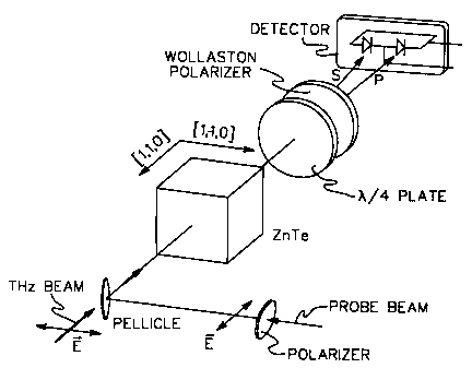
Again, when a terahertz beam illuminates an
electro-optic LiTa03 crystal with its polarization
parallel to the crystal's axis, the index of
refraction is modulated via the Pockels effect. A
femtosecond optical pulse with its polarization 45°
to the crystal's C-axis, probes the field-induced
change in the index of refraction.
Fig. 3 plots a transient waveform from an
unbiased GaAs emitter with a carefully aligned probe
beam path to achieve a velocity-matching condition.
Due to the good velocity-matching condition, an
excellent signal-to-noise ratio is attained. The
full-width-at-half-maximum (FWHM) of the main peak is
450 femtoseconds. The field measurement of the
electro-optic sensor is purely an electro-optic
process, and the system bandwidth is mainly limited
by the dispersion of the terahertz signal and the
duration of the laser pulse in the crystal, assuming
that it is phase-matched. The wide bandwidth
obtainable, minimal field perturbation, and true
temporal cross-correlation of the free-space electro-
optic system are unique characteristics of an
implementation in accordance with this invention. It
is possible to extract the true terahertz waveform
from the cross-correlation signal obtained via free-
space electro-optic sampling. This technique
CA 02255762 1998-11-20
WO 97/45747 PCT/US97/09151 -
-20-
eliminates the need for electrical contact with the
sensor crystal. Further, real-time terahertz imaging
with an electro-optic crystal plate and a CCD camera
are scientifically and commercially feasible in
accordance with the concepts presented herein.
In the implementation of Figs. I-3, the velocity
of the counter-propagating optical beam reflected
from the crystal in the projection of the terahertz
beam propagation direction matches that of the
traveling teraher.tz field. The interaction length of
the optical probe beam and the terahertz beam within
the crystal is about 200 micrometers. The nearly
velocity-matched condition reduces the walk-off
effect, increases the time response, and yields a
good signal-to-noise ratio. However, since the
terahertz beam and optical beam propagate in opposite
directions, if an array of optical beams is used
instead of a single beam, as in the case of an
imaging application, the configuration could be less
than optimal.
To overcome this, Fig. 4 depicts an alternate
embodiment wherein the optical and terahertz beams
propagate co-linearly within the electro-optic
crystal. This sensing apparatus, generally denoted
30, is a unique variation on the counter-propagating
approach discussed above. In the embodiment
depicted, the electro-optic crystal 32 is assumed to
comprise zinc tellurium (ZnTe), which has a
comparable electro-optic figure-of-merit (n3r/e) to
that of LiTa03, but without the limitations associated
with intrinsic birefringence, and a reduced
sensitivity to thermal fluctuations.
CA 02255762 1998-11-20
WO 97/45747 PCT/US97/09151 -
-21-
- Advantageously, this co-linear propagation
embodiment provides a long interaction length between
the optical probe beam and the electro-magnetic field
signal within the crystal, which in a free-space
geometry as depicted, provides excellent signal-to-
noise ratios. These ratios are much greater than
anything attainable using conventional electro-optic
sampling geometries. Fig. 4 is similar in set up to
Fig. 1 in that a laser 22 provides optical pulses
which are split 24 to provide probe pulse 16 and the
trigger signal to an emitter, after passing through
delay stage 28. The geometry differs from Fig. 1,
however, in that a beam splitter 31, such as a 1 inch
pellicle beam splitter is employed to align the
optical probe beam with a direction that the
electromagnetic field 12 is propagating. As an
example, the diameters of an unfocused terahertz beam
12 and a pre-focused optical probe beam 16 on the
electro-optic crystal 32 may be about 10 mm and 0.2
mm, respectively. This arrangement is similar to
that which would be used in a terahertz imaging
system, described further below, where the probe beam
spot (pixel size) is comparable with the terahertz
wavelength.
An 1.5 mm thick s110a oriented ZnTe crystal is
used as the electro-optic sensing head. This
orientation yields the largest electro-optic
retardation possible in a zinc blend crystal
structure, while electrical and optical incidence on
the naturally cleaved s110~ surface also produces the
best beam quality in the ZnTe. The polarizations of
both the optical probe and the terahertz beams are
said to be parallel to the s110z edge of the ZnTe
crystal for optimal electro-optic phase modulation.
CA 02255762 1998-11-20
WO 97/45747 PCT/US97/09151 -
-22-
The probe beam is optically biased with a fixed
retardation (=BC/2) by a compensator, analyzed by a
Wollaston polarizer, and measured by a balanced
photodetector as described above. During the
measurement, the power ratio of the optical
pump/probe beam is about 10,000:1.
Several photoconductively-gated pulsed microwave
emitters were tested, including centimeter-sized
photoconductive tapped antennas (transient current
source), unbiased s100>_ GaAs wafers with Brewster
angle incidence (transient photoconductive source),
and __<lllz zinc blend wafers with normal incidence
(optical rectification source). These emitters
provide microwave pulses with a pulse duration from
approximately 150 fs to 65 ps. The shortest
microwave pulses are generated from terahertz optical
rectification (slllz zinc blend crystal) while the
longest pulses are from large-end photoconductive
tapped antennas. Note that the temporal resolution
of free-space electro-optic sampling can be limited
by the laser pulse duration or the optical phono
resonance. Resolution as short as 71 femtoseconds
has been experimentally established, which is clearly
a record for electro-optic sampling.
The first set of emitters tested were
photoconductive twin-line center-fed antennas. The
antennas have two copper conductors, each resembling
an alpine-type horn. A GaAs photoconductor with
approximately a 1 mm gap was electrically contacted
to a uniform transmission-line section. The length
of the open ends of these emitters was on the order
of a centimeter, which corresponds to low frequency
resonance of several tens of gigahertz. A static
CA 02255762 1998-11-20
WO 97/45747 PCT/US97/09151 -
-23-
bias of I50 V was applied across the photoconductive
switch. Typically, the average power of the optical
trigger on the emitter was 50 mW. The measured beam
radii (1/e points into field) of the pulsed microwave
radiation and optical probe beam at the sensor
location are approximately 4 centimeters and 0.02
centimeters, respectively. This yields an estimated
cross-section-ratio of microwave beam to optical
probe beam in the sensor of 40,000:1.
Fig. 5 plots a temporal electro-optic signal
from one of the photoconductive antennas. The signal
lasts for over 1 nanosecond, and only the first 450
picoseconds are presented. The limit results from
the time delay stage having a travel distance of 7.5
centimeters, which limits the measurement to 500 ps
or correspondingly 2 GHz. With a longer delay stage
or electronic scan, the low frequency limit can be
brought down to near the laser repetition frequency,
which is 82 MHz in one embodiment of the system
discussed herein. The small features before the main
oscillation are reproducible in the representative
scans. The signal-to-noise ratio is better than
100,000:1, even with a 40,000:1 cross-section-ratio
of microwave and optical beam.
Fig. 6 shows the frequency spectrum with the
center frequency at 20 GHz and a 3 dB bandwidth of
6.3 GHz. Increased low frequency components from
larger antenna horns have been confirmed by
measurements with other antennas.
To restate, demonstrated herein is the broadband
detection capability of a co-propagating electro-
optic zinc tellurium crystal for the characterization
CA 02255762 1998-11-20
WO 97/45747 PCT/US97/09151 -
-24-
of freely-propagating, pulsed electromagnetic
radiation. In a current electro-optic sampling
system, the measured high frequency response is the
first TO phono resonance of the ZnTe sensor crystal
(5.3 THz), and the lowest frequency limit is the
laser repetition rate (82 MHz). The upper limit of
sensor frequency response is the first transverse
optical phono frequency since optical phono in
crystals will strongly absorb electromagnetic
radiation at phono frequency. It is possible to
achieve a higher frequency response by using
different electro-optic crystals. For example, InP
may be used as a rectified emitter and GaAs as a
Pockets crystal since the TO phono frequency of InP
and GaAs is 9.12 THz and 8.06 THz, respectively. To
approach measurement capabilities below that of a
laser repetition rate, a cw laser diode with an
electronically controlled time delay scan might be
employed rather than the femtosecond laser with
mechanical delay-line discussed herein.
Several electro-optic crystals with different
phono frequencies have been tested. Results indicate
that GaP is a good candidate for higher frequency
application. Fig. 7 is a plot of the temporal
waveform measured using a sllla GaP sensor crystal.
The laser has a pulse duration of 45 fs, and
currently the bandwidth is limited by the GaAs
emitter (phono at 8 THz). Fig. 8 is the frequency
spectrum and shows the cutoff frequency near 8 THz.
Absorption lines of water vapor and other gases are
clear. Since GaP has its first phono frequency at 11
THz, by using GaP as both emitter and sensor, a
bandwidth greater than l0 THz is expected. The time-
resolved 10% to 90% transient in the ring is 50 fs.
CA 02255762 1998-11-20
WO 97/45747 PCT/US97/09151 -
-25-
This is the shortest electrical transient that has
been measured coherently.
The dynamic range of free-space electro-optic
field sensor for pulsed electromagnetic wave
radiation has also been studied. With an optical
probe power spanning six decades of linearity and
excellent signal-to-noise ratio, it is feasible to
convert a far-infrared 2-D image into an optical 2-D
image. Fig. 9 is a plot of the electro-optic signal
(peak-to-peak) versus optical pump power from 0.66 mW
to 700 mW. The optical probe power was 2 mW. Since
this free-space electro-optic sampling system is
operated in the linear range (optically biased at
~r/2), the measured electro-optic signal is
proportional to the THz field, and to the optical
excitation power, assuming that the radiated field is
proportional to the optical intensity at low power.
The slope of the line fit in Fig. 9 is about 200
nA/W. Fig. 10 is a plot of the electro-optic signal
(peak-to-peak) versus optical probe power (average)
from 8 nW to 9.83 mW. The optical excitation power
on the unbiased GaAs emitter was 500 mW. Excellent
linearity of electro-optic signal, with the slope of
42 ~.A/w, is observed over six orders of probe power.
The shape of the waveform measured with 8 nW probe
power is identical to that measured at 9.8 mW. A
signal-to-noise ratio of several thousands remained
as the probe power was varied, except for optical
probe powers below 50 ~.W.
The linear behavior in both optical pump and
probe power at moderate intensity is expected. An
amplified laser system was also used as an optical
source to generate and detect THz beams. The optical
CA 02255762 1998-11-20
WO 97/45747 PCT/US97/09151 -
-26-
source is a regenerative Ti: Sapphire laser amplifier
(Coherent Rega - 9000). The pulse duration is about
200 fs, and its repetition rate is 250 kHz. The
average optical power is 0.75 W, which corresponds to
a pulse energy of 3 ~,J. Typically, the average
optical excitation power incident on the emitter is
about 250 mW, and the optical probe power is about
100 ~.W. The detection system is similar to that used
in a low optical power system. Fig. 11 is a plot of
a typical waveform measured using a ZnTe sensor (1.44
mm thick). The signal-to-ratio is greater than
10,000. The small peak before the main signal peak
(at 25 ps time location) is due to the sampling
effect of the reflected optical probe beam and THz
beam in the sensor. In contrast, sampling of the
reflected THz beam with optical probe beam starts
after the main signal peak. The maximum
photomodulation depth at quarter-wave optical bias
point is better than 80, and the contrast ratio is
better than 80o at zero-wave optical bias point. The
estimated radiation field focused at the sensor is
about 1.8 kV/cm with a static voltage of 900 V across
a 3.4 mm GaAs photoconducting emitter. The focus
spot of the THz beam is about 1 mm. In a typical
measurement, the signal-to-noise ratio can be better
than 100,000. In order to use a lock-in amplifier
which has 16 bit dynamic range, very low optical
probe power is employed to avoid an overload problem
in the lock-in. As one measurement, approximately 1-
50 ~W probe power was used. Fig. 12 is a plot of the
signal versus peak power of the pump beam. The
saturation starts at 1 MW/cm2, which is due to the
carrier screening effect.
CA 02255762 1998-11-20
WO 97/45747 PCT/US97/09151 -
-27-
Fig. 13 depicts another embodiment of a co-
propagating electro-optic sampling apparatus,
generally denoted 50, in accordance with the present
invention. In this simplified sensor arrangement,
the femtosecond optical source is assumed to comprise
a Ti: sapphire laser pumped by an Argon ion laser.
The terahertz field might be generated from an
unbiased GaAs wafer (not shown) with optical
incidence at the Brewster angle. A one inch pellicle
beam splitter 52, which is transparent to the
terahertz pulse 5l propagating from left to right,
directs the synchronized optical probe beam 53 co-
linear along the terahertz pulse. A lens (L) (f=1 m)
is placed in the probe beam path, but no lens is used
for the pump or terahertz pulse. The diameter of the
unfocused terahertz pulse and the pre-focused optical
probe beam on the electro-optic crystal 54 are about
10 mm and 0.2 mm, respectively. The probe beam spot
(0.2 mm) is comparable to the terahertz wavelength,
i.e., the wavelength of 1 THz is about 0.3 mm in air.
A quarter-wave plate (~/4) 56 is used to provide
an optical bias to the probe beam which allows the
system to be operated linearly. A Wollaston
polarizes (WP) 58 is used to convert the induced
phase retardation of the probe beam into intensity
modulation on two mutually orthogonal linearly
polarized beams. Two photodiodes (e.g., Model No.
S5533, marketed by Hamamatsu Corp. of Bridgewater,
New Jersey) connected in an unbiased mode (e. g.,
similar to a Hamamatsu Corp. custom balanced
photodiode type S1446) are used to detect optical
intensity modulation. The dark current of the
detectors is less than 0.1 pA under the unbiased
condition.
CA 02255762 1998-11-20
WO 97/45747 PCT/US97/09151 -
-28-
Several materials have been tested as sensor
crystals, including ZnTe, CdTe, ZnSe, GaAs, CdZnTe,
LiTa03, LiNb03, BGO, BTO, GaP, BaTa03 and organic DAST
crystals. Birefringent crystals (LiTa03, LiNb03 and
DAST) have large polarization fluctuation due to the
different temperature dependencies of the two
refractive indices. This polarization fluctuation
translates into intensity noise after the wollaston
polarizer. Test results have shown the ZnTe crystal
to have best sensitivity, bandwidth and stability
characteristics for the present invention.
Fig. 14 depicts a typical radiation waveform
measured by a 1.5 mm thick x110>_ oriented ZnTe
crystal. The average optical excitation power
incident on the GaAs emitter was 535 mW with an
optical probe power of 2 mW. With the use of a lock-
in amplifier (e. g., type SRS 850) with a time-
constant of 0.3 s, the waveform has a signal-to-noise
ratio (SNR) >_ 3000. If the photodetector connects
directly to an oscilloscope without the use of a
lock-in amplifier and averaging, a real-time
measurement at 40 waveforms per second with an SNR >_
50 and a 10 ps temporal window (time delay) displayed
on the digital oscilloscope can be achieved.
The use of an electro-optic sensor for terahertz
field measurements requires much less optical probe
power than a photoconductive antenna based system
such as described in the existing literature. This
is because PIN (p-type semiconductor on intrinsic
semiconductor on n-type semiconductor) photodiodes
can be used in free-space electro-optic sampling. In
general, the light sensitivity of a photodiode is
much higher than conventional ultrafast
CA 02255762 1998-11-20
WO 97/45747 PCT/US97/09151 -
-29-
photoconductive antennas. Limited carrier mobility,
coupling efficiency, and the thin optical absorbing
layer together operate to limit the responsivity of
the ultrafast photoconductive antenna.
Again, the simplicity of the detection geometry,
capability of optical parallel processing, and
excellent signal-to-noise ratio make the present
invention attractive for real-time, two-dimensional
coherent far-infrared imaging applications. For
example, a system can be constructed to convert a
spatial and temporal electric-field distribution
(far-infrared image) into an optical image by using
an electro-optic crystal plate and a photodiode
array, or a CCD camera.
One embodiment of such a system, generally
denoted 100, is depicted in Fig. 15. This system
displays on a computer monitor 102 the two-
dimensional field distribution transmitted through a
sample object 104, which might comprise a leaf. The
frequency range of the signal transmitted through the
sample object can be from gigahertz to terahertz.
After passing through the sample object, the electric
field beam is incident on a relatively large electro-
optic crystal 106, thereby changing the crystal's
index of refraction as described above. One
appropriate crystal 106 would be a s110z ZnTe
crystal.
Optical beam 110 comprises a processed laser
beam which is passed through a polarizer 112 and a
compensator 114 for processing as described above in
connection with Figs. 1 & 4. The optical probe beam
is reflected 109 to be co-linear with the electric
CA 02255762 1998-11-20
WO 97/45747 PCT/US97/09151 -
-30-
field distribution as the distribution passes through
the large electro-optic crystal 106. Again, by
establishing co-linearity, a longer radiated field -
optical beam interaction length is attained such that
the geometry is capable of use for imaging an object,
e.g., human tissue.
Note that the general concept of detection using
a counter-propagating geometry is widely used in
time-resolved far-infrared spectroscopy. However,
since the terahertz beam and optical beam are
incident from opposite directions, if an array of
optical beams is used instead of a single beam, as in
the case of an imaging application, then the
configuration is not practical. Again, to overcome
this limitation, described herein is an imaging
application wherein the optical probe and the
terahertz beam propagate co-linearly through the
electro-optic crystal. The optical probe beam probes
the electric field's spatial and temporal
distribution in the crystal. An average probe power
of 100 mW provides an image of 256 x 256 pixels at 50
pA signal current per pixel (assuming 1.5 ~W/pixel at
42 ~.A/W slope and a 800 light fill factor) with a SNR
_> 200. After passing through a polarizer 116, which
checks the polarization rotation of the optical probe
beam, the signals are collected in parallel by a CCD
camera 118 and fed digitally to computer 102 for
signal processing, i.e., data analysis (e. g., data
averaging), frequency analysis, color coding and
display of information. If the spatial resolution is
limited by the terahertz wavelength (300
micrometers), this image has a size of 7.6 x 7.6 cm.
A three inch GaAs wafer may be suitable as an
electro-optic sensor if the transmitted electro-
CA 02255762 1998-11-20
WO 97/45747 PCTlUS97/09151 -
-31-
magnetic radiation (THz pulse) is loosely focused on
the wafer. Two-dimensional or spatial imaging is
possible because the sensor crystal is relatively
large and because there is an array of detectors
simultaneously receiving many single pixel waveforms.
Fig. 16 is analogous to the imaging system of
Fig. 15 except continuous electromagnetic waves are
provided by a gunn diode 122, and a laser diode 124
provides the optical probe beam. In this
configuration, the gunn oscillator is tuned at a
specific frequency which is sensitive to the sample
under test. Radiation passing through the sample is
incident on the electro-optic sensor 100 within which
the optical probe beam, again disposed co-linear with
the radiation passing through the electro-optical
crystal, measures the field strength in the sensor.
The optical probe beam carrying the radiation field
strength information from the sensor is detected by a
CCD or diode array 118.
As noted briefly above, an alternate crystal
geometry is depicted in Fig. 17 for use in a sensing
apparatus such as Fig. 1 wherein the optical probe
signal is incident on the electro-optic crystal in a
direction counter to the direction of the
electromagnetic field passing through the crystal.
This crystal, generally denoted 200, comprises a thin
lithium tantalate plate 202 sandwiched between two
fused silica prisms 204. Fig. 18 comprises a
partially enlarged view of the optical probe signal
16 passing through crystal 200, while Fig. 19 depicts
in enlarged view one embodiment of the silica prism
204 employed in the electro-optic crystal assembly
200. As one specific embodiment, the thin lithium
CA 02255762 1998-11-20
WO 97/45747 PCT/US97/09151 -
-32-
tantalate plate 202 might be 100 microns thick, while
dimensions for prism portion 204 could comprise: x =
2mm, y = 3mm, W~ = O.lmm and WZ = -.- 1.17mm. In order
to achieve a velocity matching, the optical probe
beam and the terahertz beam should intersect at an
angle of 70.8°. For lithium tantalate, n{800nm) -
2.16,E - 43, velocity matching between terahertz wave
and an optical wave requires that the angle between
them be
6m = Cos 1 ~ ~~ COS-1 ~ 2 ~3 ~ = 70 . $° (1)
The incident angle that the fused silica and lithium
tantalate interface is:
8 = sin-1 ~ n sin l9 .2~ = sin-1' 2.16 Sin 19 .2I = 29 .3° (2)
of , 1.4 I5
While angle 9r of the fused silica prism is determined
by:
= 270- 8 = 120.4° (3)
The critical angle of fused silica is 43.6°, and
therefore the optical probe beam is guided in total
_. internal reflection mode within the prism assembly
200. Reflection in the interface between fused
silica and lithium tantalate is approximately six
percent.
Due to the waveguide effect and the dispersion
of lithium tantalate in the terahertz regime,
distortion-free detection is possible up to 3 THz.
The advantages are that: lithium tantalate has an
electro-optic coefficient lOx higher than that of
CA 02255762 1998-11-20
WO 97/45747 PCT/US97/09151 -
-33-
GaAs; after interacting with the optical beam, the
terahertz beam propagating inside the crystal no
longer contributes to the electro-optic signal since
terahertz dispersion is limited to a traveling
distance three times shorter than that of the optical
beam; the short effect of travel distance of the
terahertz beam is advantageous in connection with the
tight focusing of the silicon lens; depending on the
dimension of the crystal, the reflection-free time
window can be longer than 800 ps, which is unmatched
using other sampling geometries; and since the
optical beam scans across the terahertz beam,
frequency-dependent terahertz spot size caused by the
focusing of the silicon lens is averaged out, giving
a better frequency response.
Fig. 20 is a graph of a transient waveform
comprising a plot of electro-optic signal strength
versus time delay employing a crystal assembly such
as depicted in Fig. 17. Finally, an enhanced
embodiment of crystal assembly 200 is depicted in
Fig. 21 wherein a fused silica handle 210 attached to
the base of the crystal is provided to facilitate
handling thereof. The orientation of the c-axis of
the crystal is designated by arrows 205. As a
specific example, dimensions for handle 210 might
comprise x' ~ 3.4mm, y' - lOmm and T = 0.5mm.
One of the major advantages of free-space
electro-optic (EO) sensors for the characterization
of terahertz beams is the ultrabroad frequency
bandwidth employable. In one embodiment, applicants
have produced coherent detection of mid-infrared
terahertz beams up to 37 terahertz. This represents
a significant improvement.
CA 02255762 1998-11-20
WO 97/45747 PCT/US97/09151 -
-34-
For most EO sensors, phonon absorption imposes
an upper limit of less than 10 terahertz. Beyond the
Reststrahlen band, however, most semiconductor EO
materials are transparent all the way to near-IR.
This promotes the possibility of free-space EO
sampling in the mid-IR region. Bonvalet et al. have
demonstrated the generation of a mid-infrared
terahertz beam via optical rectification using a 15
fs laser, see "Applied Physics Letter," volume 67, pp
2907 (1995), which is hereby incorporated herein by
reference in its entirety. Combined with this
terahertz source, the EO sensors could be used in
various coherent spectroscopies.
Frequency response of EO sensors is mainly
determined by the mismatching of optical group
velocity and the frequency-dependent terahertz phase
velocity. The optimum thickness of a ZnTe sensor is
about 20 micrometers for mid-IR detection.
The experimental setup included a mode locked
Ti: sapphire laser to generate 12 fs laser pulses with
average power of about 500 mW. 350 mW of the laser
power was focused on the <110> oriented GaAs emitter
by an off-axis parabolic mirror with a 5 cm effective
focal length. The broadband terahertz radiation was
collimated and then focused by a pair of f/0.6
parabolic mirrors on the EO sensor. The laser probe
beam was combined to colinerally travel with the
terahertz beam through a 2 micrometer thick pellicle,
which has a negligible effect on laser pulse width
and terahertz beam. The EO modulation induced by the
ultrafast Pockels effect was detected by using a pair
of balanced photodiodes. Detection sensitivity of
photo-modulation (~I/I) as small as
CA 02255762 1998-11-20
WO 97/45747 PCT/US97/09151 -
-35-
2x10 'R Hz-"Z was routinely achieved. By varying the
delay between the pump and probe pulses, the time
domain waveform of the mid-IR transient can be mapped
out.
Fig. 22 shows a typical waveform obtained in a
single scan with a 300 ms lock-in time constant. A
0.45 mm thick <111> GaAs was used as an emitter and a
20 micrometer thick <110> ZnTe crystal as an EO
sensor. The terahertz pulse is clearly chirped, with
high frequency components traveling faster than the
low ones. The chirping occurs when the terahertz
pulses generated on the front surface of GaAs
propagate through the rest of the material. The
shortest period of the oscillation is 31 fs. Fourier
transform of the waveform is shown in Fig. 23, where
the highest frequency response reaches 37.3
terahertz. The gap between 5 terahertz to 10
terahertz is due to the Reststrahlen ends of ZnTe and
GaAs, while the frequency dip around 17 terahertz is
under analysis. The preliminary result demonstrates
the advantages of using the linear electro-optic
effect (Pockels effect) for the measurement of
ultrafast far-infrared to mid-infrared pulsed
electro-magnetic radiation.
The use of a high-repetition-rate (250 kHz)
regenerative amplified laser with ~,J pulse energy in
a free-space terahertz (THz) beam electro-optic
sampling system has produced a significant
improvement in both the signal-to-noise ratio (> 105)
and absolute probe beam photomodulation depth (> 8%).
Focal plane images of the electric field distribution
(strength and polarity) in dipole and quadrupole
planar photoconductive emitters are next presented.
CA 02255762 1998-11-20
WO 97/45747 PCT/US97/09151 -
-36-
Preliminary results of real-time 2-D THz images of
moving objects have been obtained.
The use of a chirped pulse regenerative
amplifier {Clark MXR) at 1 kHz repetition rate for
the detection of high power THz pulses by phase
retardation in a LiTa03 crystal has been demonstrated.
The signal-to-noise ratio (SNR), however, has been
limited by the low repetition rate, the sensor
crystal, and the geometry of the polarizer
arrangement. we now report the use of a high-
repetition rate regenerative amplified laser for the
generation and detection of free-space THz radiation
in a free-space electro-optic sampling (FS-EOS)
system using ZnTe sensor crystals. The use of a high
pulse-repetition-rate, /cJ pulse energy laser to
replace the usual low peak power laser oscillator or
low repetition rate regenerative amplifier, marks a
significant improvement over previous FS-EOS systems,
especially in the application of real-time THz
imaging of moving objects. Far-field radiation
images of dipole and a quadrupole THz photoconductive
emitters are presented as a demonstration of this
potential.
The core of the improved time-resolved THz
imaging system consists of an amplified optical
source and a FS-EOS unit. The former is a
Ti: sapphire regenerative amplifier system (Coherent
RegA 9000) with a 250 kHz repetition rate, 3 ~.J pulse
energy, and 200 fs pulse duration at 800 nm. Fig. 24
shows the sampling unit using a balanced
photodetector. This system is similar to previously
reported systems which were based on unamplified
sources; i.e.: Coherent MIRA 900; and Spectra-Physics
CA 02255762 1998-11-20
WO 97/45747 PCT/US97/09151 -
-37-
Tsunami. A 2 ~m thick pellicle beamsplitter, which
is transparent to the terahertz beam, is used to
reflect 500 of the synchronized optical probe beam
colinearly along the THz beam. The polarization of
both the THz and optical probe beams are aligned
parallel to the [1,-1,0] direction of a 1.4 mm thick
<110> oriented ZnTe sensor crystal. Following the
sensor, a quarter-wave plate is used to impart a ~r/4
optical bias to the probe beam, which allows the
system to be operated in the linear range. A
Wollaston polarizer is used to convert the THz field
induced phase retardation of the probe beam into an
intensity modulation between the two mutually
orthogonal linearly polarized beams. A pair of
silicon PIN photodiodes (EG&G C30808E) connected in a
balanced mode is used to detect the optical intensity
modulation. The typical noise current from the
balanced photodiodes, as measured by a digital lock-
in amplifier (SRS 850) is a several pA (300 ms time
constant), while the signal current from a focused
THz beam can exceed several /cA. Since the dynamic
range of the digital lock-in amplifier is only 16
bit, with a full-scale read-out current of 2 ~.A, in
order to measure dynamics close to 10,000,000 (~ 23
bit) corresponding to a maximum signal current
greater than 30 /CA, a 100 kS2 resistor, connected in
parallel to the lock-in amplifier, is used to reduce
input impedance.
Using a 2-mm GaAs photoconductive emitter with a
bias field of 2.7 kV/cm and a 1.4 mm thick <110> ZnTe
sensor, the maximum modulation depth of the probe
beam after the analyzer, measured by the balanced
photodiode is 7.7 0. These values correspond to a
peak THz field of 1.6 kV/cm in the ZnTe sensor. Fig.
CA 02255762 1998-11-20
WO 97/45747 PCT/US97/09151 -
-38-
25 plots a typical temporal signal of the THz
radiation as measured by the balanced detector
(photocurrent). The average pump power on the GaAs
photoconductor is 240 mW at normal incidence and the
average probe power (after the ZnTe crystal) is about
36 uW. The diameter of the focused THz beam and the
optical probe beam on the ZnTe crystal is about 1.5
mm and 0.6 mm, respectively. The peak-to-peak signal
current is 450 nA, and the peak-to-peak of the noise
current is less than 4 pA, with its RMS noise of 1.6
pA. To better characterize the signal-to-noise ratio
of the system, the frequency spectra of both signal
and noise are plotted in Fig. 26. From 0.1 THz to
1.2 THz, the SNR (defined as the ratio of the THz
field on/off photocurrent) is between 50,000 to
100,000. A thicker crystal, higher emitter bias
field, and a tighter focus of the THz beam in the
ZnTe sensor, results in a further increase in both
the SNR and the absolute modulation depth.
The excellent SNR and planar optical detection
enable us to perform THz imaging. Fig. 27 shows the
THz imaging setup. A 2-D distribution of the far-
infrared THz field is converted into an optical image
as sampled in the ZnTe crystal and measured by a CCD
camera. Typically, the THz beam source is a large-
aperture planar GaAs photoconductor, and a 2" silicon
lens or pair of off-axis 2" parabolic mirrors are
used to collimate and focus the THz radiation. For
the imaging experiment, due to the small full-well
capacity of the common CCD pixel, the CCD can be
easily saturated by the background light. Therefore,
the previously mentioned quarter-wave plate is
removed to reduce the background light. The largest
relative photomodulation depth with a focused THz
CA 02255762 1998-11-20
WO 97/45747 PCT/US97/09151 -
-39-
beam from this arrangement (near zero optical bias)
is better than 50%. However, with a large cross-
section THz beam, the typical photomodulation depth
is between l0e to 30% and scattered light from
defects in the ZnTe crystal is sufficient to keep the
electro-optic detection nearly linear.
Fig. 28 plots the frequency spectrum (FFT) from
one of the pixels at a focused THz point, and Fig.
28a is the temporal THz signal recorded from a single
ZO CCD pixel, where data was taken from 100 sequential
frames with a temporal step of 66.6 fs. Time-
resolved images (288x384 pixels) are obtained by
recording their consecutive frames. Unlike balanced
detection, the lock-in amplifier cannot be used with
the CCD arrays.
We have imaged the field distribution from a
planar quadrupole THz emitter. Fig. 29 shows the
quadrupole emitter where the center electrode is
biased and two side electrodes are connected to
ground. The center electrode is 1 mm wide and has a
length over 1 cm. The gaps between the side
electrodes are 1.5 mm and 2 mm, respectively. This
quadrupole geometry generates two unbalanced dipoles
with opposite polarity. The peak field distributions
are plotted in 2-D and 3-D in Fig. 29a. Fig. 29a
clearly indicates the radiation pattern and the
polarity of two opposite dipoles.
One of the most important applications of this
free-space electro-optic THz imaging method is its
ability to image moving or living objects. The
images of a moving objective at focal-plane can be
viewed at the video rate (38 frames/s). To
JUL-26-2001 18 30 RDRMS CRSSRN MRCLERN 1 613 828 0024 P.07~23
VYO 971x5747 PC'f/1JS97I09151 -
-40-
demonstrate this ability, a dipole emitCer (2x5 mrn'-
ph4CQeQnduetor) was placed about 1 cm away fxom the
fecal-plane as the THz source, and an object was '
positioned in the focal-plane. 1:'igs. 30 ~ 3oa show
the original THz imaging pattern without an object in
the imaging path, and Figs. 31 & 31a capture ari image
when an object (a wooden rod with 2 mm diameter) was
swept thxough the xHz beam path at the focal.-plane_
This system can also be used to record the
dynamic radiating process resulting from varyizxg the
bias field until breakdown- 'rhe maximum frame
transfer rate of our current CC~ (Princeton
Instrument, PentaMax'~ with a readout rate of 5
m~.llivn. pixels per second is 36 frarnes/second and aaxz
sustain up to 152 frames/second with ~x4 bin~zi.z~g.
The fastest frame transfer rate from some CCDs can
reach upwards of 2000 frames/second making it
possible to image real-time 2-D transient processes, '
including the TFIz radiation pattern from an
explosion.
In conclusion, we have demonstrated the txee-
space elactro-optic imaging using a regenerative
amplified ~.asez which combines both high repetition
rate and high pulse energy. Fn this way, slgnlficant
improvements in the j,n,ag~,ng system have been '
obtained. Results of 2-D THz images (2 cm2) at the
. focal-plane, including the real-time images of mov~.z~g
objects, have been achieved.
In an alternate aspect, the present inverr,tion '
further comprises a, ~xee-space ultrafast rnagneto-
optic sampling technique. Specif~.cally, presenfi ed
below is an ultrafast magneto-optic sampling system
~Trade~-mark
CA 02255762 2001-07-26
CA 02255762 1998-11-20
WO 97/45747 PCT/US97/09151 -
-41-
to characterize freely-propagating transient magnetic
pulses. Presented are the direct experimental
measurements of a time-resolved magnetic field
associated with a terahertz beam.
Fig. 32 depicts an apparatus for ultrafast
magneto-optic sampling in accordance with the present
invention. The setup includes a Ti: sapphire laser
regenerative amplifier (Coherent RegA) which provides
pulses of 220 fs duration and 800 nm wavelength at a
repetition rate of 250 kHz, providing 4 ~.J/pulse.
The peak power is 18 MW. The beam is split by a 95/5
beamsplitter into a time-delayed pump, which excites
a biased GaAs emitter to produce terahertz radiation,
and a weak probe beam, which measures Faraday
rotation in the magneto-optic sensor crystal induced
by the transient magnetic field. The configuration
of the magneto-optic sampling geometry differs from
the electro-optic sampling geometry. In this
experiment, the terahertz emitter is placed several
centimeters (1.5 cm to 5 cm) away from the sensor and
in a perpendicular position relative to the
propagation direction of the probe beam. Since this
technique is governed by the Faraday effect, the
magnetic component of the terahertz wave must
prorogate colinearly with the probe wave to produce
the index birefringence through,
8 ~VBLcasy
With V being the Verdent constant, B is the magnitude
of the magnetic field, L is the length of the crystal
and 'y is the angle between the direction of the
magnetic field and the direction of the probe beam
(in this case, y=0). The detection system of the
probe beam, which is similar to the detection system
JUL-26-2001 18~30 RDRMS CRSSRhI MRCLEF1N 1 613 828 0024 P.08/23
'CVO 971457~i7 PCTh(JSh7109151 -
-42-
for the electro-oQtic sampling signal., includes a .'.
pair of balanced detectors zin.d a lock-in amQlifier.
The temporal waveform of the magriet7.c signal is
recorded by seannzng the time-delay of a comQuter- -
driven translation stage,
In free-space submillimeter-wave radiation, the
pulse width of the magnetzc component is as short as
the electrzc component, and the amplitude ratio ef
the electric component to the magxcetic component in a
ZO plane wave approximation is the speed of light iri
vacuum.
Sevexal magneto-optic sensors have been tested.
One of thG sensors selected is t erbium-gallium-garnet
(TGG), which has a high vcrdet constant (i.e., v=61
rad/T~rn), a small optical absorption (~~0.0015/cm),
and a high thermal eoz7.ductivity (Ka~7.4 W/K~m) - A
small opticax absorption and a largfe thermal
conductivity provide a homogeneous Faraday rotation
in the crystal. Fig- 33 plots a temporal waveform of
the magneto-optic signal (single scan) with TGG as
the sensor. The current geometry does not satisfy
the velocity-matc~,ed condition, with a measured
risetime (7.0% to 90%) of 33 ps in Fig. 33. w~,th a
velocity-matched geometxy the temporal rasolut~-on
should be greatly improved_
Amorphous glass SP-59 behaves similar to that of
~~0, Fig_ 34 presents a 5-scan averaged response. -.
The duration of the first peak (FWHI~I) is 2i ps, with
a riseLime ( ~.0% to 90%) of Z2 ps . A Smaller O.~/i 4. -
5-8x10⁻⁵ a.s due Co the smallex Verdet constant of this
material and a shorter intEraction length of the
material. The length of the SF-59 sensor is almost
CA 02255762 2001-07-26
CA 02255762 1998-11-20
WO 97/45747 PCT/LTS97/09151 -
-43-
four times shorter than the TGG sensor. Rings in the
waveform are mainly attributable to the same criteria
discussed above. The overall response magnetic field
sensitivity of TGG is about three times greater than
SF-59.
Ultrafast magneto-optic sampling provides a
novel technique to measure freely propagating
magnetic transient signals. It is clear that free-
space magneto-optic sampling will open a new field in
the ultrafast sampling community. With the increase
of sensitivity and bandwidth, free-space magneto-
optic sampling comprises an ideal tool for the
terahertz magnetic spectroscopy. This technique
offers the coherent measurement of magnetic transient
fields, which gives precise information of the phase
and amplitude of the magnetic signal with enhanced
temporal and spatial resolution. Also, the technique
is believed useful for magnetic relaxation and
resonance studies, time-resolved studies of
magnetization transport and spin dynamics,
investigations of the intrinsic dynamics of magnetic
flux threading superconductors, as well as possible
magnetic time-domain spectroscopy for investigations
of the magnetic permeability and susceptibility of
materials, and a novel magnetic imaging corresponding
to the electro-optic imaging described above.
To summarize, a dynamic range of electro-optic
field sensors is presented herein for the coherent
detection of pulsed electromagnetic wave radiation.
In contrast to pre-existing photoconductive antenna
approaches, free-space electro-optic sampling in
accordance with this invention separates the temporal
detection from the amplitude detection by using the
CA 02255762 1998-11-20
WO 97/45747 PCT/US97/09151 -
-44-
electro-optic crystal and the photodetector as
described. This separation allows optimal
performance of both the temporal resolution and the
signal sensitivity to be achieved. Using a free-
s space electro-optic field sensor it is feasible to
convert a far-infrared spatial and temporal image
into an optical spacial and temporal image.
While the invention has been described in detail
herein in accordance with certain preferred
embodiments thereof, many modifications and changes
therein may be effected by those skilled in the art.
Accordingly, it is intended by the appended claims to
cover all such modifications and changes as fall
within the true spirit and scope of the invention.