Language selection

Search

Patent 2255961 Summary

Third-party information liability

Some of the information on this Web page has been provided by external sources. The Government of Canada is not responsible for the accuracy, reliability or currency of the information supplied by external sources. Users wishing to rely upon this information should consult directly with the source of the information. Content provided by external sources is not subject to official languages, privacy and accessibility requirements.

Claims and Abstract availability

Any discrepancies in the text and image of the Claims and Abstract are due to differing posting times. Text of the Claims and Abstract are posted:

  • At the time the application is open to public inspection;
  • At the time of issue of the patent (grant).
(12) Patent Application: (11) CA 2255961
(54) English Title: ELECTRONIC COMPONENT, IN PARTICULAR A COMPONENT USING ACOUSTICAL SURFACE ACOUSTIC WAVES
(54) French Title: COMPOSANT ELECTRONIQUE, EN PARTICULIER COMPOSANT A ONDES ACOUSTIQUES DE SURFACE (COMPOSANT SAW)
Status: Dead
Bibliographic Data
(51) International Patent Classification (IPC):
  • H03H 9/05 (2006.01)
  • H03H 9/10 (2006.01)
(72) Inventors :
  • STELZL, ALOIS (Germany)
  • KRUGER, HANS (Germany)
  • PAHL, WOLFGANG (Germany)
(73) Owners :
  • SIEMENS MATSUSHITA COMPONENTS GMBH & CO. KG (Germany)
(71) Applicants :
  • SIEMENS MATSUSHITA COMPONENTS GMBH & CO. KG (Germany)
(74) Agent: FETHERSTONHAUGH & CO.
(74) Associate agent:
(45) Issued:
(86) PCT Filing Date: 1997-05-23
(87) Open to Public Inspection: 1997-12-04
Examination requested: 2002-02-26
Availability of licence: N/A
(25) Language of filing: English

Patent Cooperation Treaty (PCT): Yes
(86) PCT Filing Number: PCT/DE1997/001055
(87) International Publication Number: WO1997/045955
(85) National Entry: 1998-11-20

(30) Application Priority Data:
Application No. Country/Territory Date
196 21 127.1 Germany 1996-05-24

Abstracts

English Abstract


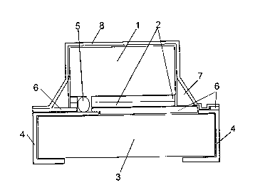
An electronic component, in particular a component using surface acoustic
waves, with a system of components (1, 2) mounted on a base plate (3) and with
electrical contacts made, where a protective layer (8) is provided on the
components side, facing away from the connecting zone between the components
system (1, 2) and the base plate (3); the protective layer (8) forms a tight
seal against environmental influences to the base plate (3) for the components
system (1, 2).


French Abstract

Composant SAW comprenant un système de composants (1, 2) montés électriquement en contact sur un substrat (3), caractérisé en ce qu'une couche protectrice (8) est prévue sur le côté du composant opposé à la zone de connexion entre le système de composants (1, 2) et le substrat (3), et en ce que la couche protectrice (8) forme un scellage étanche vis-à-vis des influences de l'environnement, pour la liaison dudit système de composants (1, 2) au substrat (3).

Claims

Note: Claims are shown in the official language in which they were submitted.


Claims

1. An electronic component, in particular a component
operating with surface acoustic waves - SAW component -, in
which a component system (1,2; 10, 11, 12) which comprises
electrically conductive structures (11, 12) on a substrate (1;
10) is mounted such that it makes electrical contact on a
baseplate (3; 13) and which has a protective coating which
shields the component system (1, 2; 10, 11, 12) against
environmental influences,
characterized in that
the protective coating (8; 19) is provided on that side of the
component which faces away from the connecting region between
the component system (1, 2; 10, 11, 12) and the baseplate (3;
13) and which forms a seal against environmental influences
for the component system (1, 2; 10, 11, 12) toward the
baseplate.
2. The component as claimed in claim 1,
characterized in that
the component system (1, 2; 10, 11, 12) is mounted on the
baseplate (3; 13) using flip-clip technology.
3. The component as claimed in claim 1,
characterized in that
the component system (1) is mounted on the baseplate (3) and
is electrically connected by means of wire contacts (31).
4. The component as claimed in claim 1 or 2,
characterized in that
the protective coating (8) is applied, toward the baseplate
(3), to that side of the substrate (1) which faces away from
the connecting region between the component system (1, 2) and
the baseplate (3), such that a seal which is proof against
environmental influences is formed toward the baseplate (3).
5. The component as claimed in one of claims 1 to 3,
characterized in that
a plastic covering (18) is provided on the component system
(10, 11, 12), and the protective coating (19) is applied to
the plastic covering (18) toward the baseplate (13), in such a
manner that a seal which is proof against environmental
influences is formed toward the base-plate (13).
6. The component as claimed in one of claims 1 to 5,
characterized in that
the protective coating (8; 19) is a coating containing metal.
7. The component according to one of claimed 1 to 5,
characterized in that
the protective coating (8; 19) is a metal coating.

8. The component according to one of claims 1 to 5,
characterized in that
the protective coating (8; 19) is a coating formed from a
plurality of partial coatings.
9. The component according to claim 8,
characterized in that
at least one partial coating is a metal coating.
10. The component according to claim 8
characterized in that
at least one partial coating is a glass coating..
11. The component according to claim 10
characterized in that
the glass coating is the lower partial coating of a partial
coating sequence.
12. The component according to one of claims 1 to 11
characterized in that
a corrosion protective coating is provided on the protective
coating (8; 19).
13. The component according to one claims 1 to 12,
characterized in that
an adhesive coating is provided under the protective coating
(8; 19).
14. The component according to one of claims 1 to 13,
characterized in that
the metallic part of the protective coating (8; 19) is made
contact with electrically.

Description

Note: Descriptions are shown in the official language in which they were submitted.


11~20/1998 11: 53 9251101 LERNER GREENBERG PAGE 02


? ~ r
~;~ 96 P 1514 ' ,~ ~.,L,~
Deacription

~lectronic co~po~ent, in par~icular a component operating with
~urface acou~tic wave~ - SAW component -

~he pre~ent invention relat~ to an electronic componen~, lnparticular a comro~e~t operatin~ with ~urface acOUBtie wa~e~ -
SAW eompone~t - according to the pream~le of paten~ claim 1.

It is known for electronic c~ro~t~ to be protectcd by
protective coating~ agaln~t environmental infl~ e~, for
example at~acks by chemical ~b~tance~, such as moisture. For
example, US PS 3 g38 873 de~cribe~ the protection o~
semico~ductor ~L~J~-entfi by prntectl~e coatings o~ silicon
nitride, al~ n~m oxide and mixed ~ili~ate~ ~uch aB a~ nllm
~ilic~te. Tn thi~ case, the ~rotectivc coatin~ i~ applied
directl~ onto ~he ~-ye~em o~ the ~emicond~tor component. ~rhe
t~r~ co~por~nt ~ystem in t~i~ ca~e mean~ the ~ub~ate which
contain~ ~he ac~ive electronic parts of the ~orron~nt. In
other words, the ~ L~onent ~e~em ie thu~ the c~,~onent
excludin~ any hou~ing contai n; ng it.

In certain electronic ~ o~,ts, it may not be ~en~ible, and
may e~en be dam~ging to the component function, to apply a
protective coating o~ the ~aid type onto the co~ron~ sy~em
~t~elf. Thi~ he case, ~or example, with comp~ent~
ope~atin~ with eur~ace acouetic waves, ~ince a protective
coating applied on~o the ~f,.-.L,o.~n~ sys~em of such co~ronents
c~n ad~reely a~ect t~e propagation o~ eur~ace aoou~tic
wavee. ~nother example of thi~ would ~e ~ensore for mechani~al
etreeses, ~ince ,e-h~n;cal ~or~e~ ca~ed by the proteetive
cc~ating irl the ~en~or ~;y~tem may inl~luence the detection of
mechanical e~res~e~ to be mea~ured.

--1--


CA 02255961 1998-11-20

11/20~1998 11:53 9251101 LERNER GREENBERG PAGE 03


The pre~ent invention i~ ba~ed on the object of ~pe~ifying one
option for protecting ele~tronic co~ron~nt~ againfit
environmental influence~ witho~t the adver~e e~e~s ~hich can
occur from protectlve coating~ applled onto co~p~ne~t s~stem-
~

Thi~ object i~ achieved accordi~g to the in~ention in the ca~eof an ele~ronic component of the type mentioned initially, ~y
the ~eature~ i~ the de~cripti~e part of patent ~laim 1.

~evelop~ent~ of the invention are the ~ubject mat~er of
dependent claimq.

The invention i~ explained in more d~tail in the ~ollowing
text wlth reference to exemplaxy c~oA~ments which are
illu~rated in the ~igure~ of the drawings. Jn thi~ ~a~,
Fi~ures ~ to 3 ~how, schem~tically, variou~ e~h~;~ent~ o~
electronic r~po~ent~ designe~ accor~ing to ~e inven~ion.

In the ca~e o~ the e-~ho~ent of a~ electronic compo~ent
accordin~ to Figure 1, a comroTler-t sy~;tem i8 mounted on a
ba~eplate 3 ~uch that it m~kes ele~trical contact. The
component ~y~em ie illu~trated ~chematlcally by a ~UbBt~ate
and an lnsulating frame 2 whi~h ~urro~ds ele~rically
conductive ~tructures ~which are ~ot ~hown). The electrically
CQn~ tive ~truc~ure~ may be, for example, lnterdigital
converters, re~onatoxs or re~lector~ for SAW ~u ~ nt~

The term ~baQeplate" for the purpo~e~ of ~he present invention
mean~ any s~b~tra~e with conductor tracks or interco~nect~
~ounte~ on it, on a pla~tic, gla~ or cera~ic baee. r~ tor
trac~ 4 are pro~ided on the ba~eplate 3 and make contact via
bump~ 5 wi~h t~e (not illu~rate~) cond~ctive stru~ure~ on
the ~ub~trate 1 of the ~.,.~o~ent ~y~tem. Such electrical


CA 02255961 1998-11-20


11~20~1998 11: 53 9251101 LERNER GREENBERG PAGE 04


contact compri~es the ~o-called flip-chip moun~ing which i5
known per se.

An in~ulating coatin~ 6, whi~h i~ co~ro~ed, fo~ example, o~
epoxy re~;in 4r gla~;E;, is provided on the baseplate 3, between
the conductor tracks 4 and the f~ame 2 which ~urround~ the
electrically conductive ~tr~ctures on ~he sub~trate l
~inally, in the ~o~necting region between the ~ nt sy~tem
1, 2 and the ba~eplate 3, a ~urrounding frame 7 i~ pro~ided
which may be, for example, an adhe~ive, a pot~ing reein or a
pre~ing ~ und. Thi~ ~urround iQ provided in particular to
ab~orb ~hear foxces which occur ~ a re~ult of different
thermal -Y~n~ion levels in ~he comrone~t ~y~tem and ~he
ba~eplate, and could mechanically a~ver~ely affect the
' electrical contact between the ele~rically conducti~e
~tructure~ on the ~ub~trate 1 ~nd the ron~.-ctor tracks 4 on
the baseplate 3 via the bump~ 5.

According to the lnvention, a pro~ective coatin~ 8 i5 pro~ided
on the component ~ide whi~h face~ away ~rom the ~s~ting
regio~ between the comron~nt sy~tem 1, 2 a~d the ba~plate 3,
and form~ a ~eal, which i~ proof again~t en~iL~ al
influence~r for the ~G~onent sy~tem toward the baeeplate. As
will be expl~in-1 in more detail in the following text, thl~
protecti~e coa~ing 8 ~ay be formed in variou~ ways.

In the ca~e of ~he embodimen~ of an ~W ~ nt ae ~ho~n in
Figure 2, an SAW ~"~on~nt ~y6te~ i~ ~ormed by ,~G 0~ a
piezoelectric ~ub~trate lo as well a~ r~ ctive ~tructure~ 11
(which are provided on thi~ ~ub~trate 10~ and connecting
~ur~ces 12 - pads - for the con~lrtive ~t~ucture~ 1}. The
electrically c~d~ctive ~truc~ures 11 may once A~- ~ n ~e, for
example, inte~digital converter~, re~onatore or reflectorc.
The c~n~lctive ~tructure~ 11 an~ the pad~ 12 are ~urrounded by


CA 02255961 1998-11-20

11~2E)~1998 11: 53 92511E~1 LERNER GREE~BERG PAGE 05


an in~ulating frame 21, according to the embodimen~ ~hown in
Figure 1. The illu~ration of an SAW co~pon~nt ~y~tem 10, 11,
12 in Figure 2 i~, once again, only of a ~chematic nature. The
complete con~truction of such a co~ron~nt ~t~m ~or SAW
component~ i~ know~ per ~e and will thu~ not be explAi n~ in
any more de~ail here.

In addition, a b~eplate 13 is pro~i~ed, on who~e ~ide facing
the co~ron~n~ sy~tem lO, 1~ co~ tor trac~ 14 are
pro~ided, wi~h bumps ~5 located o~ them, via which electric~l
coneact i~ m~de between the co~p~nt and the pad~ 12 The
con~truction of the baseplate 13 i~ not limited to two layer~.
Basepla~e~ with ~ore than two layer~ may also be u~ed.

The ele¢trical contact~ can be brought out of the co~nen~ by
pa~ing the conduc~or track~ 14 around the basepla~e 13, a~ i~
illu~trated on ~he left-hand ~ide of Figure 2, or by the
ba8eplate being ~onn~ted via bu~hings 16-1, 16-~, 16-3 to
CQ~~ tor track~ 17 on the o~t~3ide of the! ba~eplate 13. The
con~i~uratlon of the electrical hn~ng 16-l, 16-2, 16~3
off~e~ in the vertical dlrec~ion i~ ueed to prevent ingre~e of
chem~cal fiub~tance~ which adver~ely affe~t compo~ent
operation, that is to ~ay the off~et design o~ the bU~hin~
ensure~ a gas seal fro~ the out~ide of the ba~eplate 13. If
the condu~tor tracks 14 are pa~sed around the bafieplate 13 a~d
are co~n~ed to a pad 12 via bump~ ~5, an insulating coating
~0 i9 required between the ~onA~ctor track 14 and a protective
coating 1~, which 1~ de~ribed in the following text.

The ~ ~t sy~em 10, ll, 1~ is covered ~y a pla~tic ~heet
18 on ~he hasepl~te 13. ~his ~verin~ lB may be forme~ by
potting refiinQ, pressing ~.,.~o~nd~ or ~hermopl~tic8


CA 022SS961 1998-11-20


11~20~1998 11:53 9251101 LERNER GREENBERG PAGE 06


Accordin~ to the invent~on, a protective coating 19 according
~o ~he invention i~ provided on the cover 1~, on the eide
facing away fxom the connecting region be~ween the co~ron~t
~tem 10, ll, 12 and the baseplate 1~, and ~orm~ a sea~,
which i~ proof a~ain~t en~i~ - tal in~luence~, towar~ the
b~eplate 13.

A~ has already been G~ated ab~ve, the protective coating 8 ac
~hown in Figure 1, and lg a~ ohown in Figure z, can be formed
in various way~ . According to one e~ho~ ~ ~ent, it may be a
co~ting cont:~ining a metal or a completely n~etal coa~cing.
Fur~hennore, (although thl~: is not illul3tratecl 3pecifically in
Figure~; 1 and 2) it can algo ~e ~ormed ~y a plur~lity of
partial coatin~, at lea~t one o~ which i~ a metal coating.
Furthermore, one of the partial coati~g-~ may ~e a gla~
coa~ing which may be, ~n parti~ular, the lower partial coatin~
of ~ partial coatlng sequence. The metal~ which m~y be u~ed
include çopper, nickel o~ gold. A metal coatin~ may be
applied, for example, by vapor depo~ition, ~acuum
metallizatlon, elec~rochemical treatmen~ or ~ n~tion If
reguired, a corros~on proteCtive coating ~rhich i6 ~ot
illuYtrat~d speci~ically) may in t~i~ case be provide~ on th~
metal coating. Fur~hermore, an adheHi~e coating Iwhich lç
likewi~ not illustrated) may be pro~ided un~er ~e metal
coating.

illu~trated on t~e basi~ of the e~ho~;~ent ~hown in
Figure 2, the pro~c~i~e coatin~ 19, that i~ to say
~peci~ically its me~allic part, c:an ~e rnade contact wi~h
elec~rically, so t~at the protective çoating 19 ic not onl~ a
coating which provide~ protec~ion again~t envi ~ u ental
influence~, but a~ the ~ame tlm~ al~o forms a radio-frequen~y
chield I~or the c~ n~r,t fiy~;tem lO, 11, 12. To t.hi~ nd, the


CA 0225596l l998-ll-20

11~20~1998 11:53 9251101 LERNER GREENBERG PAGE ~7


protective coating 1~ is connected to a ~o~ ctor track 14 on
the ~a:3eplate 13, a~ i~; illue;trated by a link :22 in Figure 2.

Fig~re 3, in whi~h identical part~ to ~ho~e in Flgure~ 1 and 2
are provided with ~he ~ame re~erence ~ymbol~, chow~ an
embodiment in which the ~r~ent ~tem haQ wire con~act~. In
~his ca6e, the Yubstrate 1 i~ moun~ed on the ba~eplate 3 ~y
mean~ o~ a suitable joint, for example an adhe~ive ~O. Wire
contact i~ made ~ia contact wire~ 31 to the conduc~or tra~k-~ 4
on the ~3ide facing away from ~he moun~ing region.

~n ~his emboc~ nt as~ well, a pla~3tic sheath la with a
protective coating 19 according to the inven~ion i~ provided,
corres~p~n-l~ ng to that ~;hown in Figure 2


CA 02255961 1998-11-20


Representative Drawing
A single figure which represents the drawing illustrating the invention.
Administrative Status

For a clearer understanding of the status of the application/patent presented on this page, the site Disclaimer , as well as the definitions for Patent , Administrative Status , Maintenance Fee  and Payment History  should be consulted.

Administrative Status

Title Date
Forecasted Issue Date Unavailable
(86) PCT Filing Date 1997-05-23
(87) PCT Publication Date 1997-12-04
(85) National Entry 1998-11-20
Examination Requested 2002-02-26
Dead Application 2004-05-25

Abandonment History

Abandonment Date Reason Reinstatement Date
2003-05-23 FAILURE TO PAY APPLICATION MAINTENANCE FEE

Payment History

Fee Type Anniversary Year Due Date Amount Paid Paid Date
Registration of a document - section 124 $100.00 1998-11-20
Application Fee $300.00 1998-11-20
Maintenance Fee - Application - New Act 2 1999-05-25 $100.00 1999-04-16
Maintenance Fee - Application - New Act 3 2000-05-23 $100.00 2000-05-08
Maintenance Fee - Application - New Act 4 2001-05-23 $100.00 2001-05-08
Request for Examination $400.00 2002-02-26
Maintenance Fee - Application - New Act 5 2002-05-23 $150.00 2002-05-03
Owners on Record

Note: Records showing the ownership history in alphabetical order.

Current Owners on Record
SIEMENS MATSUSHITA COMPONENTS GMBH & CO. KG
Past Owners on Record
KRUGER, HANS
PAHL, WOLFGANG
STELZL, ALOIS
Past Owners that do not appear in the "Owners on Record" listing will appear in other documentation within the application.
Documents

To view selected files, please enter reCAPTCHA code :


To view images, click a link in the Document Description column. To download the documents, select one or more checkboxes in the first column and then click the "Download Selected in PDF format (Zip Archive)" or the "Download Selected as Single PDF" button.

List of published and non-published patent-specific documents on the CPD .

If you have any difficulty accessing content, you can call the Client Service Centre at 1-866-997-1936 or send them an e-mail at CIPO Client Service Centre.


Document
Description 
Date
(yyyy-mm-dd) 
Number of pages   Size of Image (KB) 
Representative Drawing 1999-02-11 1 5
Claims 1999-01-19 3 74
Claims 1998-11-20 2 84
Abstract 1998-11-20 1 54
Description 1998-11-20 6 254
Drawings 1998-11-20 3 41
Cover Page 1999-02-11 1 41
Prosecution-Amendment 1999-01-19 4 113
PCT 1998-11-20 24 790
Assignment 1998-11-20 4 175
Prosecution-Amendment 2002-02-26 2 57
Fees 2000-05-08 1 40