Note: Descriptions are shown in the official language in which they were submitted.
CA 022~984 1998-12-14
Title of the Invention
PROCESS FOR PRODUCING AN ACTUATOR F.T.T~M~NT AND
MICRODEVICE ~
Field of the Invention
The present invention relates to a process for
producing an actuator element. More particularly, the
present invention relates to a process for producing an
actuator element capable of curving or deforming an ion
exchange resin molding. Further, the present invention
relates to a process for producing a lead wire which is
electrically connected to an electrically operating
device such as any of various sensors, a motor or an
electrostatic or a polymeric actuator so that the lead
wire is most suitably used in the transmission or
receiving of signals and the supply of power. This
electrically working device arranged at an end of an
instrument inserted in an organ, such as a catheter
used, for example, to inject a medicinal liquid into a
blood vessel or other hollow organs or to insert a tool
for observation and treatment, a guide wire inserted
through the inside of the catheter and used to guide the
catheter to the target site or a medical tube for use in
an endoscope, etc.; or arranged at an end of a guide for
use in the inspection and repair of the piping and
CA 022~984 1998-12-14
eauipment set in industrial facilities, buildings, etc.
Also, the present invention relates to a working jig
therefor.
Still further, the present invention relates to a
microdevice for use in the inspection and repair of the
piping and branched pipeline disposed in industrial
facilities and equipment and buildings, and a
microdevice for use in the ex~m;n~tion and treatment in
the medical field, for example, a microdevice such as
forceps, scissors, a clamp, a snare, a laser knife, a
spatula or a clip for use in microsurgery such as
ophth~1m;c surgery or peritoneoscopic surgery. In
particular, the present invention relates to a
microdevice so constructed that it can be oscillated in
arbitrary directions. Moreover, the present invention
relates to a micromachine provided with the above
microdevice.
Backaround of the Invention
Recently, there is an enhanced demand for a
miniaturized, lightweight and highly flexible actuator
in the fields of medical eauipment, industrial robots,
micromachines and the like.
When the actuator is thus miniaturized, the
friction and viscous force are domin~nt over the
CA 022~984 1998-12-14
inertial force. Therefore, it has been difficult to
employ the means for converting energy to motion with
the use of inertial force, such as a motor or an engine,
as the power source of a microactuator. Accordingly,
the operating principles based on electrostatic
attraction, piezoelectricity, ultrasonic wave, shape
memory alloy and polymer expansion/contraction have been
proposed for the microactuator.
The actuator of the electrostatic attraction type
operates by attracting, for example, a plate or rod
becoming an electrode toward a counter electrode, and,
for example, one which bends an electrode by applying a
voltage of about 100 V between the electrode and the
counter electrode disposed with a spacing of about tens
of microns is known. The piezoelectric actuator
operates by applying a voltage of some volts to a
piezoelectric element of a ceramic such as barium
titanate so that the element is expanded and contracted,
and one capable of controlling a nm-unit displacement is
known. The ultrasonic actuator operates by combining
frictional force with the ultrasonic vibration generated
by the piezoelectric element or the like, or by
effecting a runoff. The actuator of the shape memory
alloy type operates by temperature change with the use
of the marked change of the configuration of the shape
CA 022~984 1998-12-14
memory alloy depending on temperature. The actuator of
the polymer expansion/contraction type operates with the
use of the expansion/contraction of~the polymer
depending on the temperature or change of pH and change
of the concentration of environmental chemical
substance.
However, these microactuators have drawbacks in
that there is restriction in their respective operation
environments, the response is unsatisfactory, the
structure is complicated and the flexibility is poor.
For example, for the operation of the actuator of the
polymer expansion/contraction type, the solution in
contact with the polymer must be replaced by the
solution containing other salt. Therefore, it has been
difficult to employ this actuator in the use requiring a
small size and a rapid response. In contrast, an
actuator element comprising an ion exchange membrane and
electrodes coupled to surfaces of the ion exchange
membrane and adapted to apply a potential difference to
the ion exchange membrane in the hydrous state so that
the ion exchange membrane is curved or deformed has been
proposed as one which can be easily miniaturized,
realizes rapid response and operates with small electric
power (see Japanese Patent Laid-open Publication No.
4(1992)-275078).
CA 022~984 1998-12-14
This actuator element is characterized by
comprising an ion exchange resin membrane and metal
electrodes coupled to surfaces thereof in mutually
insulating relationship and by being adapted to apply a
potential difference between the metal electrodes while
the ion exchange resin membrane is in the hydrous state
so that the ion exchange resin membrane (as ion exchange
resin molding) is curved or deformed.
In this actuator element, the electrodes are formed
on the surfaces of the ion exchange resin molding by
chemical plating, electroplating, vacuum deposition,
sputtering, coating, press bonding, fusion bonding or
other methods. For example, in the chemical plating,
the surfaces of the ion exchange membrane are subjected
to etching, bearing of a plating catalyst and immersion
in a plating bath, so that the surfaces of the ion
exchange membrane are plated to thereby have electrodes
formed thereon.
However, the actuator element having the electrodes
formed by the above methods has a drawback in that the
displacement level is not satisfactory. Therefore, it
has been desired to develop an actuator element capable
of realizing a greater displacement level and ensuring
rapid response.
CA 022~984 1998-12-14
On the other hand, as shown in Fig. 28, it is
common practice to arrange microdevice 301, such as any
of various sensors, a motor or an actuator capable of
carrying out mechanical operation and mechanism,
e.g., an electrostatic actuator, at front end portion
303 of guide 302, such as a medical tube or a medical
wire, of, for example, a catheter or an endoscope for
the purpose of performing ~reatment and observation in a
hollow organ, such as an intricate blood vessel.
In order to supply electric power to the above
microdevice 301 or to carry out the transmission and
receiving of signals, electric wire (lead wire) 304
comprising a copper wire of small diameter furnished
with an insulating coating of a resin is arranged inside
the tube or wire 302 or along the inner or outer wall
thereof. The electric wire 304 is connected to control
operating unit 305 such as an analyzer.
Also, the reliability enhancement and maintenance
easiness are now major tasks in accordance with the
upgrading and complication of plants, such as power
generating facilities, and mechanical systems, such as
aircraft engines. A microdevice such as any of various
sensors or an actuator is arranged at an end of a tube
or wire as a guide in order to carry out, for example,
inspection or repair, without disassembly, in an
CA 022~984 1998-12-14
extremely limited space, such as the inside of a plant
piping system or aircraft engine. In this application
as well, the same construction as in the medical
application is employed.
The above guide may be inserted in, for example, a
vital peripheral blood vessel or an intricate branched
pipe of an equipment piping. Therefore, it is now
required to reduce the diameter and size of the guide.
However, the above arrangement of a lead wire
comprising a copper wire furnished with an insulating
coating of a resin inside a tube as a guide has
drawbacks in that, for meeting and sustaining the
objective to inject a medicinal liquid into a blood
vessel or to use in observation and treatment, the size
of the guide is likely to become too large because of
the need to secure, for example, a medicinal liquid
path, or the medicinal liquid path inside the tube
becomes too narrow, thereby lowering the effect of
injecting the medicinal liquid. Moreover, fitting the
microdevice of minute size with the lead wire involves
difficult working, and arranging the lead wire of small
diameter in the tube requires extremely precision and
accurate working, thereby causing a productivity
lowering.
CA 022~984 1998-12-14
Therefore, a method has been proposed which,
referring to Fig. 29, comprises coating the surface
(outer wall) 312 of substrate 311 of a tube or wire as
an intraorgan insertion tool with a conductive material
such as a metal by the ion assist vapor deposition
process to thereby form deposition coating 313 and,
thereafter, repeatedly scanning the surface of the
substrate having its outer wall coated with the
conductor, along the longitudinal direction of the
substrate 311, with laser beam machine 314 using, for
example, excimer laser so that the surface of the
substrate 311 is irradiated with laser beam 315 to
thereby remove parts of the coating and, hence, form
insulating channels 316 with the result that a plurality
of conductive paths 317, 318 in mutually insulated
relationship are formed on the surface of the substrate
311 (see Japanese Patent Laid-open Publication No.
8(1996)-131545). In the method of Japanese Patent Laid-
open Publication No. 8(1996)-131545, the conductive
paths 317, 318 on the upper surfaces thereof are plated
with a metal by the electroplating or electroless
plating so that the electric resistance of the
conductive paths 317, 318 is lowered.
However, this method, in which the substrate
surface is coated with the conductor by the vapor
CA 022~984 1998-12-14
deposition of a metal, requires a large apparatus for
carrying out the vapor deposition of a metal, such as a
vacuum deposition apparatus, and the vapor deposition
operation is complicated. Therefore, the method is not
suitable for continuous production. Further, the
control of the bonding strength between the vapor
deposition layer of a metal and the substrate surface is
difficult, and the flexibility of the vapor deposition
layer or plated layer is so poor that the followup
thereof to substrate elongation is not satisfactory.
Therefore, there has been a problem such that a layer
separation from the substrate surface is caused by the
insertion or push in an intricate or branched minute
target site or the withdrawal therefrom or by the
rotational torque with the result that the conductivity
is lowered.
Moreover, in the method disclosed in Japanese
Patent Laid-open Publication No. 8(1996)-131545, the
insulating channels 316 are formed by repeatedly
scanning the substrate 311, along the longitudinal
direction thereof, with the laser beam machine 314 so
that the surface of the substrate 311 is irradiated with
the laser beam 315 to thereby remove parts of the
coating. Therefore, unless laser irradiation is
performed while accurately positioning and fixing the
CA 022~984 1998-12-14
1 0
substrate, there would be the danger of short
circuiting of conductive paths. However, in the
Japanese Patent Laid-open Publication No. 8(1996)-
131545, there is no disclosure teaching or suggesting
the method of positioning and fixing the substrate.
On the other hand, in the contemporary medical
field, there is a demand for high medical technology for
m;n;m;zing the pain inflicted on patients at the time of
ex~m;n~tion or treatment to thereby relieve the physical
and psychic burden on patients. The development of
medical equipment for meeting the above demand is
indispensable.
In the technology of microsurgery such as
ophthalmosurgery, peritoneoscopic surgery or
microangiosuturing surgery, as shown in Fig. 30,
microdevice 400 comprising slender guide member body 404
constituting an intraorgan insertion part and, connected
to an end thereof, therapeutic microtool 402 such as
forceps, scissors, a clamp, a snare, a laser knife, a
spatula or a clip has been provided as the above medical
equipment. This microdevice is independently used as
medical equipment.
The guide member body 404 of the microdevice 400 is
composed of a tube of thermoplastic resin with some
flexibility and, according to necessity, has its
CA 022~984 1998-12-14
circumferential surface wound by a metal wire
(generally, stainless steel wire) in order to increase
the rigidity thereof. The microtool 402 such as a
therapeutic knife connected to an end of the guide
member body 404 is guided to lesion, and the lesion is
extirpated or resected thereby. At the insertion of the
microdevice in an organ, the end portion thereof is
inserted in an intricate or branched minute part and
guided to the target site while manually manipulating
the end position by transmitting a rotational torque or
pushing or pulling the endoscope body by means of the
operating part on the handy side.
Also, referring to Fig. 31, the above microdevice
400 may be fitted in internal space for microdevice 414
of a mounting hole formed inside tubular endoscope body
412 and may be used as micromachine 410.
In this micromachine, the endoscope body 412 is
also composed of a tube of thermoplastic resin with some
flexibility and, according to necessity, has its
circumferential surface wound by a metal wire
(generally, stainless steel wire) in order to increase
the rigidity thereof. For example, at the insertion of
the endoscope body 412 in an organ, the end portion
thereof is inserted in an intricate or branched minute
part and guided to the target site while manually
CA 022~984 1998-12-14
12
manipulating the end position by transmitting a
rotational torque or pushing or pulling the endoscope
body by means of the operating part~on the handy side.
Upon the guidance of the endoscope body 412 to the
target site, the therapeutic microtool 402 of the
microdevice 400 and the end of the guide member body 404
thereof are protruded from the internal space for
microdevice 414. The therapeutic microtool 402 such as
a therapeutic knife connected to the end of the guide
member body 404 is guided to lesion, and the lesion is
extirpated or resected thereby. In Fig. 31, numeral 416
denotes an irradiation lens and numeral 417 a
photographic lens.
On the other hand, the reliability enhancement and
maintenance easiness are now major tasks in accordance
with the upgrading and complication of plants, such as
power generating facilities, and mechanical systems,
such as aircraft engines. Thus, when, for example,
inspection or repair is performed, without disassembly,
in an extremely limited space, such as the inside of a
plant piping system or aircraft engine, use is also made
of a microdevice with similar structure, comprising a
slender guide member body and, connected to an end
thereof, a microtool such as any of various sensors or a
CA 022~984 1998-12-14
repair tool. Further, use is made of a micromachine
furnished with the microdevice.
However, with respect to the independent use of the
microdevice of the above structure, for example, in
ophth~lm;c surgery, the outer diameter of the guide
member body constituting the intraorgan insertion part
of the microdevice is about 0.9 mm, and the guide member
body has a straight form. Therefore, the freedom
thereof is low, and it is difficult to guide the
microtool, such as a therapeutic knife, connected to an
end of the guide member body to lesion or the like to
thereby resect or extirpate the same. The operator must
have high degrees of expertise and experience, and there
is limitation in the manual skill with the result that
physical and psychic burden may be inflicted on the
patients.
On the other hand, with respect to the use of the
microdevice fitted in the mounting hole provided inside
the endoscope body as a micromachine, similar problem is
encountered in the operation of leading the endoscope
body to the target site in an organ and, thereafter,
guiding the microtool such as a therapeutic knife
connected to an end of the guide member body to lesion
to thereby resect or extirpate the same.
CA 022~984 1998-12-14
14
These are the same in, for example, a piping system
or engine interior of plants, such as power generating
facilities, and mechanical systems,~such as aircraft
engines, so that the consumption of labor and time has
been substantial in the repairing thereof.
Summary of the Invention
The present invention is intended to solve the
above problems of the prior art. Accordingly, it is an
object of the present invention to provide a process for
producing an actuator element which exhibits a large
displacement extent and a large displacement force, has
a simple structure, can be easily miniaturized, exhibits
a high response speed and is flexible.
It is another object of the present invention to
provide a process for producing a lead wire, in which
conductive lines of a conductive coating can
continuously be applied to a surface of a lead wire
substrate such as a tube or wire efficiently by simple
procedure without the need to use a large apparatus.
It is still another object of the present invention to
provide a process for producing a highly conductive lead
wire which comprises a substrate and conductive lines
bonded to a surface thereof with a high strength, the
conductive lines being excellent in flexibility, being
CA 022~984 1998-12-14
excellent in the follow-up to substrate elongation and
not peeled from the substrate surface by the insertion
or push in intricate or branched minute target sites or
the pull therefrom or by the rotational torque.
It is a further object of the present invention to
provide a process for producing a lead wire, in which,
in the formation of insulating zones conducted by
-irradiating a surface of a lead wire substrate with, for
example, laser beam to thereby remove part of a coating,
the irradiation with laser, etc. can be performed with
the substrate accurately positioned and fixed to thereby
enable avoiding, for example, mutual short circuiting of
conductive lines. It is still a further object of the
present invention to provide a working jig therefor.
It is still a further object of the present invention to
provide a microdevice which realizes freely guiding a
microtool connected to an end of a guide member body to,
for example, lesion in an organ or break-down part of a
piping of mechanical system to thereby enable
facilitating and perfectly carrying out an appropriate
surgery or repair and to provide a micromachine
furnished with the microdevice.
The present invention has been made with a view
toward solving the above problems of the prior art and
attaining the above objects. Therefore, in one aspect
CA 022~984 1998-12-14
16
of the present invention, there is provided a process
for producing an actuator element, the above actuator
element comprising an ion exchange resin molding and
metal electrodes which are formed in mutually insulated
relationship on surface of the ion exchange resin
molding, the above ion exchange resin molding adapted to
be curved or deformed upon application of a potential
difference between the metal electrodes while the ion
exchange resin molding is in hydrous state, which
process comprises the steps of:
(l) causing the ion exchange resin molding to
adsorb a metal complex in an aqueous solution, and
(2) reducing the adsorbed metal complex with a
reducing agent so that a metal is precipitated on
surface of the ion exchange resin molding to thereby
form a metal electrode.
The formation of a metal electrode by the above
process enables obtaining an actuator element which has
a simple structure, can be easily miniaturized, exhibits
a high response speed and exhibits a large displacement
extent.
It is preferred that a gold or platinum complex be
used as the metal complex. The use of a gold or
platinum complex enables obtaining an actuator element
exhibiting a large displacement extent.
CA 022~984 1998-12-14
In the present invention, upon formation of the
metal electrode, the ion exchange resin molding
preferably has its counter ion replaced by at least one
cation selected from the group consisting of Li+, Na+
and Cu2+. The displacement extent of the obtained
actuator element can further be increased by the cation
replacement.
The process for producing a lead wire according to
the present invention comprises the steps of:
coating surface of a lead wire substrate of an
insulating material with a conductive solution to
thereby form a conductive thin-film layer on the
surface, and
irradiating the lead wire substrate, in one
direction therealong, with light so that the conductive
thin-film layer is removed by the irradiation working to
thereby form insulating zones and thus form a plurality
of mutually electrically insulated conductive lines
along the lead wire substrate.
In this process, it is preferred that the coating
with the conductive solution be performed by a dip
coating and that the conductive solution be a conductive
solution of Au or Ag.
This process, because it is only required to coat
the surface of the lead wire substrate with the
CA 022~984 1998-12-14
18
conductive solution, enables continuously providing
conductive lines efficiently by simple procedure without
the need to use a large apparatus. ~Furthermore, a
highly conductive lead wire can be provided thereby, in
which the bonding strength between conductive lines and
substrate surface is excellent, the conductive lines
being excellent in flexibility, being excellent in the
follow-up to substrate elongation and not peeled from
the substrate surface by the insertion or push in
intricate or branched minute target sites or the pull
therefrom or by the rotational torque.
It is preferred that the lead wire substrate be in
tubular form. In this instance, the lead wire per se
can be used as a guide, such as a medical tube or a
medical wire, for a catheter, an endoscope, etc., so
that a medicinal liquid path can be ensured and a size
miniaturization can be attained. Further, in the
fitting of the above lead wire in a fine microdevice,
the lead wire fitting operation is easy to thereby
ensure high productivity.
It is preferred that the irradiation working be
performed by laser from the viewpoint that noncontacting
working can be effected and, hence, an outer wall having
a curved surface such as that in tubular form can be
easily worked.
CA 022~984 1998-12-14
1 9
Moreover, the process for producing a lead wire
according to the present invention is characterized in
that, in the irradiation working, the lead wire
substrate is fitted and fixed in a fixing channel
provided in an irradiation working jig, and surface of
the lead wire substrate, which is exposed from the
irradiation working jig, is subjected to the irradiation
worklng .
This enables providing a lead wire in which mutual
short circuiting of the conductive lines can be avoided
because, in the formation of insulating zones by partial
removal of the coating by irradiating the surface of the
lead wire substrate with, for example, laser beam, the
formation of the insulating zones can be performed with
the lead wire substrate accurately positioned and fixed.
It is preferred that the irradiation working jig
comprise a plate base frame having its upper surface
provided with a fixing channel, this fixing channel
adapted to fix a lead wire substrate so that a surface
of the lead wire substrate is subjected to irradiation
from upside. This construction enables securely
positioning and fixing the lead wire substrate in the
fixing channel.
In the present invention, preferably, the
irradiation working jig comprises a pair of base frames
CA 022~984 1998-12-14
arranged upside and downside, these base frames having
matching faces provided with fixing channels, the above
base frames provided with irradiation slits extending
from the fixing channels to upper and lower surfaces of
the base frames, and the lead wire substrate is fixed
between the fixing channels by closing the base frames
together and is at its surface subjected to irradiation
working through the irradiation slits. This enables
accurately forming two insulating zones at the upper and
lower surfaces of the lead wire substrate, respectively.
Further, preferably, the irradiation working jig
comprises four base frames arranged upside right, upside
left, downside right and downside left, these base
frames having matching faces provided with fixing
channels, the above base frames provided with
irradiation slits extending from upper, right, lower and
left surfaces of the base frames to the fixing channels,
and the lead wire substrate is fixed between the fixing
channels by closing the base frames together and the
lead wire substrate is at its surface subjected to
irradiation working through the irradiation slits. This
enables accurately forming a total of four insulating
zones at the upper, right, lower and left surfaces of
the lead wire substrate, respectively.
CA 022~984 1998-12-14
The working jig of the present invention is a jig
for irradiation working for use in producing a lead
wire, comprising a plate base frame~having its upper
surface provided with a fixing channel, this fixing
channel adapted to fix a lead wire substrate so that a
surface of the lead wire substrate is subjected to
irradiation from upside.
This enables providing a lead wire in which mutual
short circuiting of the conductive lines can be avoided
because, in the formation of insulating zones by partial
removal of the coating by irradiating the surface of the
lead wire substrate with, for example, laser beam, the
formation of the insulating zones can be performed with
the lead wire substrate accurately positioned and fixed.
It is preferred that the fixing channel be defined by a
fixed plate fastened to an upper surface of the base
frame and a channel width regulating plate arranged,
movably toward the fixed plate, on the upper surface of
the base frame. The reason for the preference is that
the lead wire substrate can be securely fixed.
Further, the working jig of the present invention
may comprise a pair of base frames arranged upside and
downside,
the above base frames having matching faces
provided with fixing channels, the above fixing channels
CA 022~984 1998-12-14
adapted to fix a lead wire substrate therebetween by
closing the base frames together,
the above base frames provided~with irradiation
slits extending from upper and lower surfaces of the
base frames to the fixing channels,
the above irradiation slits adapted to perform
irradiation working of a surface of the lead wire
substrate therethrough. This enables accurately forming
two insulating zones at the upper and lower surfaces of
the lead wire substrate, respectively.
Still further, the working jig of the present
invention may comprise four base frames arranged upside
right, upside left, downside right and downside left,
the above base frames having matching faces
provided with fixing channels, the above fixing channels
adapted to fix a lead wire substrate therebetween by
closing the base frames together,
the above base frames provided with irradiation
slits extending from upper, right, lower and left
surfaces of the base frames to the fixing channels, the
above irradiation slits adapted to perform irradiation
working of a surface of the lead wire substrate
therethrough. This enables accurately forming a total
of four insulating zones at the upper, right, lower and
left surfaces of the lead wire substrate, respectively.
CA 022~984 1998-12-14
The microdevice of the present invention comprises:
a slender guide member body;
a therapeutic tool connected to a front end of the
guide member body;
a polymeric actuator arranged in the vicinity of
part of the connection; and
an actuator operation control unit electrically
connected to the actuator through a lead wire extending
along a longitudinal direction of the guide member body,
wherein the polymeric actuator comprises an ion
exchange resin molding and at least one pair of
electrodes, provided in positions interposing the ion
exchange resin molding, and
wherein an arrangement is made such that the ion
exchange resin molding is deformed by selective
application of a voltage through the lead wire to the
pair of electrodes by means of the operation control
unit so that the therapeutic tool connected to the front
end of the guide member body can be oscillated in any
arbitrary direction.
Moreover, the micromachine of the present invention
comprises the above microdevice fitted in an internal
space of a tubular slender guide member body, wherein an
arrangement is such that the microdevice can be
CA 022~984 1998-12-14
24
protruded through an opening formed at a front end of
the slender guide member body.
When the microdevice is inserted in an organ or a
piping system of mechanical system and guided to the
target site, by virtue of the above arrangement, the
therapeutic tool connected to the front end of the guide
member body can be oscillated in any arbitrary
direction, so that it does not become a hindrance and is
free from inadvertently injuring the organ interior or
piping. Furthermore, when the microdevice must be
operated, it can be guided to lesion in an organ and
failure site in a piping system of mechanical system, so
that the operation and repair can be carried out easily
and securely.
Brief Descri~tion of the Drawinas
Fig. 1 is a schematic sectional view of one form of
actuator element obtained by the process of the present
invention, which is in the state of having no voltage
applied thereto;
Fig. 2 is a schematic sectional view of one form of
actuator element obtained by the process of the present
invention, which is in the state of having a voltage
applied thereto;
CA 022~984 1998-12-14
Fig. 3 is a schematic diagram showing an example of
application of one form of actuator element obtained by
the process of the present invention;
Fig. 4 is a schematic enlarged view of an essential
part of Fig. 3;
Fig. 5 is a schematic diagram showing another form
of actuator element obtained by the process of the
present invention;
Fig. 6 is a schematic diagram explaining one mode
of step of coating with a conductive solution, conducted
in the process for producing a lead wire according to
the present invention;
Fig. 7 is a schematic diagram explaining one mode
of step of forming insulating zones by irradiation
working, conducted in the process for producing a lead
wire according to the present inventioni
Fig. 8 is a schematic diagram explaining another
mode of step of coating with a conductive solution,
conducted in the process for producing a lead wire
according to the present invention;
Fig. 9 is a perspective view of one form of working
jig for use in the process for producing a lead wire
according to the present invention;
. .
CA 022~984 1998-12-14
26
Fig. 10 is a perspective view of another form of
working jig for use in the process for producing a lead
wire according to the present inventioni
Fig. 11 is a perspective view of still another form
of working jig for use in the process for producing a
lead wire according to the present invention;
Fig. 12 is a perspective view of a further form of
working jig for use in the process for producing a lead
wire according to the present invention;
Fig. 13 is a sectional view on the line A-A of Fig.
12;
Fig. 14 is a partially enlarged sectional view of
still a further form of working jig for use in the
process for producing a lead wire according to the
present invention;
Fig. 15 is a perspective view of still a further
form of working jig for use in the process for producing
a lead wire according to the present invention;
Fig. 16 is a sectional view on the line B-B of Fig.
15i
Fig. 17 is a schematic diagram of another form of
irradiation working apparatus for use in the present
nventlon;
Fig. 18 is a partially cutaway perspective view of
the first form of micromachine fitted with the
.. ...
CA 022~984 1998-12-14
microdevice of the present invention applied to the
medical field, especially, microsurgery field;
Fig. 19 is a schematic diagram~of one form of
microdevice of the present inventioni
Fig. 20 is a schematic diagram of an essential part
of the microdevice of the present invention shown in
Fig. 19;
Fig. 21 is a schematic diagram showing the
micromachine furnished with one form of microdevice of
the present invention which is in the state of resecting
and extirpating lesion in an organ;
Fig. 22 is an enlarged perspective view of an
essential part of another form of microdevice of the
present inventioni
Fig. 23 is a schematic view of still another form
of microdevice of the present invention;
Fig. 24 is a schematic diagram of an essential part
of the microdevice of the present invention shown in
Fig. 23;
Fig. 25 is an enlarged perspective view of an
essential part of a further form of microdevice of the
present invention;
Fig. 26 is an enlarged sectional view on the line
C-C of Fig. 25;
CA 022~984 1998-12-14
28
Fig. 27 is an enlarged sectional view on the line
D-D of Fig. 25;
Fig. 28 is a schematic diagram~of the conventional
medical tube;
Fig. 29 is a schematic diagram explaining the
process for producing the conventional lead wire;
Fig. 30 is a perspective view of the conventional
microdevice; and
Fig. 31 is a perspective view of the micromachine
provided with the conventional microdevice.
Detailed Descri~tion of Preferred Embodiment
Embodiments of the present invention will be
described in detail below with reference to the
drawings.
Figs. 1 and 2 are schematic sectional views of the
most suitable form of actuator element obtained by the
process of the present invention. In this form of
actuator element, actuator element 1 comprises slender
rectangular plate of ion exchange resin molding 2 and
electrodes 3a, 3b arranged in mutually insulating
relationship on opposite surfaces of the ion exchange
resin molding 2. A potential difference is applied
between the electrodes 3a, 3b while the ion exchange
resin molding 2 is in a hydrous state, so that the ion
CA 022~984 1998-12-14
29
exchange resin molding 2 is curved or deformed.
Ends of a pair of lead wires 4a, 4b are respectively
electrically connected to the electrodes 3a, 3b, and the
other ends of the lead wires 4a, 4b are connected to
power source 5.
The shape of the ion exchange resin molding 2 is
not limited to the above rectangular plate, and may be,
for example, a membrane, a column or a cylinder.
The ion exchange resin for forming the above ion
exchange resin molding 2 can be an anion exchange resin,
a cation exchange resin or an amphoteric ion exchange
resin. Of these, the cation exchange resin is
preferably used because the extent of displacement of
the actuator element can be large.
The above cation exchange resin can be a resin such
as polyethylene, polystyrene or a fluororesin having,
introduced therein, a functional group such as a
sulfonate group or a carboxyl group. Especially, a
cation exchange resin comprising a fluororesin having,
introduced therein, a functional group such as a
sulfonate group or a carboxyl group is preferred. Among
the above cation exchange resins, those having an ion
exchange capacity of 0.8 to 2.2 meq/g, especially, 1.4
to 1.8 meq/g are still preferred. The use of the cation
exchange resin having such an ion exchange capacity
. ......... .. . ..
CA 022~984 1998-12-14
enables further increasing the extent of displacement of
the actuator element.
In the present invention, a metal complex is
adsorbed, on the ion exchange resin molding in an
aqueous solution, and the metal complex having been
adsorbed on the ion exchange resin molding is reduced by
a reducing agent to thereby precipitate a metal on
surfaces of the ion exchange resin molding. Thus, metal
electrodes are formed.
As this metal complex, any of gold, platinum,
palladium, rhodium and ruthenium complexes can be used.
Of these, gold and platinum complexes are preferred
because the extent of displacement of the actuator
element can be large.
The adsorption of the above metal complex onto the
ion exchange resin molding is effected by immersing the
ion exchange resin molding in an aqueous solution
containing the metal complex.
The reduction of the metal complex is effected by
immersing the ion exchange resin molding having the
metal complex adsorbed thereonto in an aqueous solution
containing a reducing agent.
Although depending on the type of employed metal
complex, the reducing agent can be selected from among,
for example, sodium sulfite, hydroxylamine
CA 022~984 1998-12-14
31
hydrochloride, hydrazine and potassium borohydride.
According to necessity, an acid or an alkali may be
added in the reduction of the metal~complex.
Upon the reduction of the metal complex adsorbed on
the ion exchange resin molding, a metal precipitates on
surfaces of the ion exchange resin molding, thereby
forming metal electrodes.
In the present invention, surfaces of the employed
ion exchange resin molding may be roughened prior to the
formation of the metal electrodes. The roughening of
membrane surface can be conducted by the use of, for
example, sandblasting or sand paper treatment. The
degree of the roughening of the surface may be such that
the surface layer is shaved.
This roughening increases the area of contact of
the surfaces of the ion exchange resin molding and the
later formed electrodes to thereby enable increasing the
extent of displacement of the actuator element.
Further, in the present invention, the employed ion
exchange resin molding may be subjected to:
(1) water treatment in which the ion exchange resin
molding is heated in boiling water;-
(2) hydrochloric acid treatment in which the ionexchange resin molding is held in dilute hydrochloric
acid of about 25% by volume;
CA 022~984 1998-12-14
(3) NaOH treatment in which the ion exchange resin
molding is held in an aqueous sodium hydroxide solution
of about 0.1 N;
(4) alcohol treatment in which the ion exchange
resin molding is immersed in an alcohol such as methanol
or ethanol; or
(S) autoclave treatment in which the ion exchange
resin molding is heated at 110 to 150~C in an autoclave.
With respect to the reduction of the metal complex
adsorbed on the ion exchange resin molding, it is
presumed that a metal precipitation occurs at the
surface of the ion exchange resin molding at which the
metal complex contacts the reducing agent and,
accordingly, the metal complex lying in the internal
part of the membrane moves toward the vicinity of the
membrane surface (toward the precipitated metal) and is
reduced to thereby attain the desired metal
precipitation. The metal precipitation is made in not
only the surface of the ion exchange resin molding but
also the internal part close to the surface, so that the
area of contact of the ion exchange resin molding and
the metal electrode would be larger-than in the
conventional chemical plating process. Therefore, the
actuator element obtained in the present invention
CA 022~984 1998-12-14
exhibits a greater extent of element displacement than
that of the conventional actuator element.
After the electrode formation,~the ion exchange
resin molding is generally washed with pure water to
thereby remove unprecipitated metal complex and the
reducing agent. The insulation between the electrodes
can be effected by cutting the edges of the ion exchange
resin molding having the metal electrodes formed
thereon. Further, the insulation between the electrodes
can be effected by irradiating the ion exchange resin
molding having the metal electrodes formed thereon with
laser beam or electron beam to thereby shave parts of
the metal electrodes with the result that insulating
zones are disposed between the electrodes.
Moreover, the ion exchange resin molding having the
electrodes formed thereon may be subjected to the above
treatments (1) to (5).
Furthermore, additional electrode layers may be
disposed on the formed electrodes. The additional
electrode layers can be formed by chemical plating,
electroplating, vacuum deposition, sputtering, coating,
press bonding, fusion bonding or other methods. These
additional electrode layers may be either identical with
or different from the metal layers formed on the
surfaces of the ion exchange resin molding.
CA 022~984 1998-12-14
34
Still further, the ion exchange resin molding
having the electrodes formed thereon may have its
counter ion replaced by, for example, Li+, Na+, Cu2+, H+,
Ca2+, Fe3+ or Mg2+. Of these ions, the replacement is
preferably conducted by Li+, Na+ or Cu2+. This counter
ion replacement can be effected by immersing the ion
exchange resin molding having the electrodes formed
thereon in an aqueous solution of LioH, NaOH, etc.
At the operation of the thus obtained actuator
element, it is requisite that the ion exchange membrane
should be in the hydrous state. The terminology
"hydrous state" used herein means that the actuator
opera~es in not only water but also highly humid
atmosphere.
With respect to the mechanism of operation of the
above actuator element, it is presumed that, when a
potential difference is applied between opposite
surfaces of the ion exchange resin molding which are in
mutually insulating relationship, positive (+) ions 4
lying in the ion exchange resin molding move to the
negative electrode side as shown in Fig. 2 and,
entrained by the ions, water molecules move in the
membrane with the result that a water content difference
occurs between the positive electrode side and the
negative electrode side. Thus, it is presumed that the
.
CA 022~984 1998-12-14
increase in water content causes a swelling and the
decrease in water content causes a shrinkage, so that
the ion exchange resin molding is curved.
The thus obtained actuator element can have a
displacement of about 0.5 to 3 times the length of the
actuator element within a period of seconds at the
application of a direct current voltage of 0.1 to 3 V
between the electrodes. This actuator element can
flexibly operate in water.
An example of application of this actuator element
can be found in the guide of Fig. 3.
In this application example, guide wire 11 as a
guide comprises linear member 12 composed of, for
example, a slender tube of synthetic resin or stainless
steel and actuator element 13 connected to an end of the
linear member 12.
The above actuator element 13 comprises ion
exchange resin molding 14 shaped into a relatively
slender rectangular plate and, disposed on both sides
thereof, a pair of electrodes 15a, 15b formed by the
process of the present invention. Application of a
voltage to the electrodes 15a, 15b causes the actuator
element 13 to curve in two directions.
Ends of a pair of lead wires 16a, 16b are
electrically connected to the electrodes 15a, 15b,
CA 022~9X4 1998-12-14
36
respectively. The lead wires 16a, 16b are positioned
inside the linear member 12 and extend along the entire
length of the linear member 12, and~the other ends of
the lead wires 16a, 16b are connected to operation
control unit 17.
This operation control unit 17 is fitted with
operating lever 18 which enables switching operation.
The electrode of the current from power source 20 which
flows through the pair of lead wires 16a, 16b can be
switched by means of double-pole double-throw switch 19
disposed inside the operation control unit 17 in
accordance with the manipulation made by the operating
lever 18.
That is, referring to Fig. 4, when the double-pole
double-throw switch 19 is arranged in the position
indicated by the full line, the lead wires 16a and 16b
are connected to the positive electrode and the negative
electrode, respectively. On the other hand, when the
double-pole double-throw switch 19 is rearranged from
the neutral position as indicated by the two-dot long
and two short dashes line in accordance with the
manipulation made by the operating lever 18 of the
operation control unit 17, contrarily, the lead wires
16a and 16b are connected to the negative electrode and
the positive electrode, respectively.
CA 022~984 1998-12-14
As apparent from the above, the actuator element 1
can arbitrarily and positively be deformed by
manipulating the positive electrode~and the negative
electrode.
Furthermore, cylindrical actuator element 40 as
shown in Fig. 5 can be produced by the process of the
present invention.
In the production of this cylindrical actuator
element 40, first, a metal complex is adsorbed on
cylindrical ion exchange resin molding 41 by the above
procedure. The metal complex is reduced by a reducing
agent to thereby precipitate a metal on the surface of
the ion exchange resin molding 41 so that a metal layer
is formed.
Subsequently, the cylindrical ion exchange resin
molding 41 having its outer surface furnished with the
metal layer, at the outer surface, is irradiated with
laser beam from a laser beam machine to thereby remove
the metal layer at the irradiated part. Thus, channel-
shaped insulating zones 42 and a plurality of mutually
electrically insulated metal electrodes 43a, 43b, 43c,
43d are formed.
In the actuator element of Fig. 5, ends of lead
wires 44a, 44b, 44c, 44d are electrically connected to
the metal electrodes 43a, 43b, 43c, 43d, respectively.
CA 022 j j984 1998- 12- 14
38
The ion exchange resin molding 41 can be curved in four
directions by applying a voltage to electrodes 43a, 43c
disposed opposite to each other with the ion exchange
resin molding 41 interposed therebetween and to
electrodes 43b, 43d disposed opposite to each other with
the ion exchange resin molding 41 interposed
therebetween. Further, the curving directions can be
combined with each other to thereby enable a rotation.
These metal electrodes may be arranged on an inner
circular face of the ion exchange resin molding.
- Example 1
A 0.2 mm-thick fluororesin ion exchange resin
molding (Nafion 117 produced by E.I. DuPont de Nemours &
Co., Inc., having an ion exchange capacity of 0.9 meq/g)
was sandblasted with the use of alumina particles (no.
800), thereby roughening the surface of the ion exchange
resin molding. After the surface roughening, sandblast
particles and other dirt were removed from the ion
exchange resin molding by ultrasonic cleaning.
Thereafter, the ion exchange resin molding was boiled in
an aqueous 25% by volume hydrochloric acid solution for
30 min and boiled in pure water for 30 min to thereby
remove hydrochloric acid therefrom.
CA 022~984 1998-12-14
39
After the above boiling, the ion exchange resin
molding was immersed in an aqueous solution of
platinum/amine complex for 6 hr to thereby cause the ion
exchange resin molding at its internal part to adsorb
the platinum/amine complex. Thereafter, the ion
exchange resin molding was immersed in an aqueous
solution of sodium borohydride at 40 to 65~C for 5 hr to
thereby reduce the platinum/amine complex with the
result that platinum was precipitated on the surface of
the ion exchange resin molding.
The ion exchange resin molding having platinum
precipitated on its surface was further immersed in an
aqueous solution of platinum/amine complex, and an
aqueous solution of hydroxylamine hydrochloride and an
aqueous solution of hydrazine were added thereto and
heated at 40 to 60~C for 5 hr to thereby reduce the
platinum/amine complex. Thus, platinum growing plating
was performed on the surface of the ion exchange resin
molding, thereby accomplishing an electrode formation.
After the electrode formation, the resultant ion
exchange resin molding was boiled in an aqueous 25% by
volume hydrochloric acid solution for 30 min and boiled
in pure water for 30 min to thereby remove hydrochloric
acid therefrom.
CA 022~984 1998-12-14
The above ion exchange resin molding was immersed
in a lM aqueous LiOH solution for 6 hr to thereby
replace the counter ion by Li+ and cut into strips of 1
mm width. Thus, an actuator element was obtained.
The extent of bending displacement of a front end
portion exhibited when a voltage of 2 V was applied to
the obtained actuator element was measured by the use of
a laser displacement meter. The extent of bending
displacement was evaluated in terms of the displacement
extent per 10 mm of the element length.
The results are given in Table 1.
Example 2
An actuator element was produced in the same manner
as in Example 1, except that a lM aqueous NaOH solution
was used in place of the lM aqueous LioH solution to
thereby replace the counter ion by Na+. The extent of
bending displacement thereof was evaluated in the same
manner as in Example 1. The results are given in Table
1.
Example 3
An actuator element was produced in the same manner
as in Example 1, except that an ion exchange resin
molding exhibiting an ion exchange capacity of 1.4 meq/g
, _ . .
CA 022~984 1998-12-14
was used, and that a lM aqueous NaOH solution was used
in place of the lM aqueous LioH solution to thereby
replace the counter ion by Na+. The extent of bending
displacement thereof was evaluated in the same manner as
in Example 1. The results are given in Table 1.
Exam~le 4
An actuator element was produced in the same manner
as in Example 1, except that a lM aqueous CuSO4 solution
was used in place of the lM aqueous LioH solution to
thereby replace the counter ion by Cu2+. The extent of
bending displacement thereof was evaluated in the same
manner as in Example 1.
The results are given in Table 1.
Exam~le 5
The roughened ion exchange resin molding which was
obtained in the same manner as in Example 1 was boiled
in an aqueous 25% by volume hydrochloric acid solution
for 30 min and boiled in pure water for 30 min to
thereby remove hydrochloric acid therefrom.
The resultant ion exchange resin molding was
immersed in an aqueous solution of gold complex
(dichlorophenanthrolinegold chloride) to thereby cause
the ion exchange resin molding at its internal part to
CA 022~984 1998-12-14
42
adsorb the gold complex. The ion exchange resin molding
having adsorbed the gold complex was immersed in an
aqueous solution of sodium sulfite and heated at 40 to
80~C for 5 hr to thereby reduce the gold complex with
the result that gold was precipitated on the surface of
the ion exchange resin molding to thereby attain an
electrode formation.
The ion exchange resin molding, on which the
electrode was formed, was immersed in lN sulfuric acid
for 30 min and further immersed in pure water to thereby
remove sulfuric acid therefrom.
The above ion exchange resin molding was immersed
in a lM aqueous LioH solution for 6 hr to thereby
replace the counter ion by Li+ and cut into strips of 1
mm width. Electrode connection was effected, thereby
obtaining an actuator element.
The extent of bending displacement of the obtained
actuator element was evaluated in the same manner as in
Example 1.
The results are given in Table 1.
Comparative Exam~le 1
The surface of the same ion exchange resin molding
as employed in Example 1 was subjected to chemical
CA 022~984 1998-12-14
43
plating so that a platinum electrode was formed on the
surface of the ion exhange resin molding.
The ion exchange resin molding, on which the
electrode was formed, was immersed in a lM aqueous LioH
solution for 6 hr to thereby replace the counter ion by
Li+ and cut into strips of 1 mm width, in the same
manner as in Example 1. Electrode connection was
effected, thereby obtaining an actuator element.
The extent of bending displacement of the obtained
actuator element was evaluated in the same manner as in
Example 1.
The results are given in Table 1.
Com~arative Exam~le 2
The surface of the same ion exchange resin molding
as employed in Example 1 was subjected to a vacuum
deposition of platinum so that a platinum electrode was
formed on the surface of the ion exchange resin molding.
The ion exchange resin molding, on which the
electrode was formed, was immersed in a lM aqueous LioH
solution for 6 hr to thereby replace the counter ion by
Li+ and cut into strips of 1 mm width, in the same
manner as in Example 1. Electrode connection was
effected, thereby obtaining an actuator element.
CA 022~984 1998-12-14
44
The extent of bending displacement of the obtained
actuator element was evaluated in the same manner as in
Example 1.
The results are given in Table 1.
Comparative Exam~le 3
The surface of the same ion exchange resin molding
as employed in Example 1 was subjected to sputtering so
that the surface was furnished with a platinum
electrode.
The ion exchange resin molding, on which the
electode was formed, was immersed in a lM aqueous LioH
solution for 6 hr to thereby replace the counter ion by
Li+ and cut into strips of 1 mm width, in the same
manner as in Example 1. Electrode connection was
effected, thereby obtaining an actuator element.
The extent of bending displacement of the obtained
actuator element was evaluated in the same manner as in
Example 1.
The results are given in Table 1.
Com~arative Example 4
The surface of the same ion exchange resin molding
as employed in Example 1 was coated with a conductive
ink containing fine particles of platinum so that a
CA 022~984 1998-12-14
platinum electrode was formed on the surface of the ion
exchange resin molding.
The ion exchange resin molding, on which the
electrode was formed, was immersed in a lM aqueous LiOH
solution for 6 hr to thereby replace the counter ion by
Li+ and cut into strips of 1 mm width, in the same
manner as in Example 1. Electrode connection was
effected, thereby obtaining an actuator element.
The extent of bending displacement of the obtained
actuator element was evaluated in the same manner as in
Example 1.
The results are given in Table 1.
Exam~le 6
An actuator element was produced in the same manner
as in Example 1, except that a lM aqueous HCl solution
was used in place of the lM aqueous LioH solution to
thereby replace the counter ion by H+, and the extent of
bending displacement thereof was evaluated in the same
manner as in Example 1.
The results are given in Table 1.
Example 7
An actuator element was produced in the same manner
as in Example 1, except that a lM aqueous CaC12 solution
CA 022~9X4 1998-12-14
46
was used in place of the lM aqueous LioH solution to
thereby replace the counter ion by Ca2+, and the extent
of bending displacement thereof was~evaluated in the
same manner as in Example 1.
The results are given in Table 1.
Exam~le 8
An actuator element was produced in the same manner
as in Example 1, except that a lM aqueous FeC13 solution
was used in place of the lM aqueous LioH solution to
thereby replace the counter ion by Fe3+, and the extent
of bending displacement thereof was evaluated in the
same manner as in Example 1.
The results are given in Table 1.
Exam~le 9
An actuator element was produced in the same manner
as in Example 1, except that a lM aqueous MgC12 solution
was used in place of the lM aqueous LioH solution to
thereby replace the counter ion by Mg2+, and the extent
of bending displacement thereof was evaluated in the
same manner as in Example 1.
The results are given in Table 1.
Example 10
CA 022~984 1998-12-14
47
An actuator element was produced in the same manner
as in Example 1, except that the ion exchange resin
molding was immersed in an aqueous solution of rhodium
complex in place of the immersion in the aqueous
solution of platinum/amine complex to thereby form a
rhodium electrode. The extent of bending displacement
thereof was evaluated in the same manner as in Example
1.
The results are given in Table 1.
1 0
Table 1
Electrode Counter Method of Extent of
metal ion formingdisplacement
electrode (mm)
Example 1Pt Li+ 3.2
Example 2Pt Na+ 2.8
Example 3Pt Na+ 4.1
Example 4Pt Cu2+ 2.5
Example 5Au Li+ 2.9
Comp.Ex.lPt Li+Chemlcal 0.2
Comp.Ex.2Pt li+ Vacuum 0.2
Comp.Ex.3Pt Li+Sputtering O.l
Comp.Ex.4Pt Li+ lnk
Example 6Pt H+ 1.1
Example 7Pt Ca2+ 0.4
Example 8Pt Fe3+ . 0.7
Example 9Pt Mg2+ 0.6
ExamplelOPt Li+ 0.4
...... ...... . .
CA 022~984 1998-12-14
48
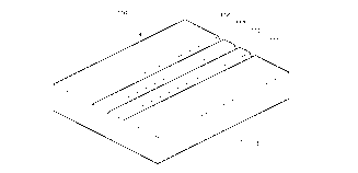
Fig. 6 is a schematic diagram explaining one mode
of step of coating with a conductive solution, conducted
in the process for producing a lead~wire according to
the present invention. Fig. 7 is a schematic diagram
explaining one mode of step of forming insulating zones
by irradiation working, conducted in the process for
producing a lead wire according to the present
invention.
Referring to Fig. 6, numeral 101 denotes a lead
wire substrate which constitutes the body of the lead
wire of the present invention. The lead wire substrate
101 has the shape of a tube and is composed of, for
example, a polyolefin resin such as polyethylene or
polypropylene, a polyurethane resin, a polyester resin
or a polycarbonate resin. The lead wire substrate 101
may be composed of any highly flexible polymeric
materials other than these, and the materials are not
particularly limited. Although the size of the lead
wire substrate 101 can also be appropriately changed
according to the purpose of the use, it is preferably in
the range of, for example, about 0.1 to 20 mm in outside
diameter, 0.003 to 5 mm in thickness and 500 to 2000 mm
in length in the use in, for example, the medical field.
The lead wire substrate 101 of the above construction is
dipped in dip coating bath 103 in which conductive
CA 022~984 1998-12-14
49
solution 102 is placed. Thereafter, the lead wire
substrate 101 is taken out from the dip coating bath 103
and dried, so that conductive thin-film layer 104 is
formed on the outer wall lOla of the lead wire substrate
101.
In place of the above dipping of the lead wire
substrate 101 in the dip coating bath 103 to thereby
form the conductive thin-film layer 104 on the outer
wall lOla of the lead wire substrate 101, as shown in
Fig. 8, the lead wire substrate 101 can be passed
through hole 103a provided at the bottom of the dip
coating bath 103 and pulled upward in the arrowed E
direction, so that the conductive thin-film layer 104
can be continuously formed on the outer wall lOla of the
lead wire substrate 101.
The paste material constituting the principal agent
of the conductive solution 102 is preferably selected
from among, for example, epoxy, polyimide, polyester,
acrylic, vinyl and phenol resins.
The conductive material as a constituent of the
conductive solution is, for example, a conductive metal
such as Au, Ag, Cu, Al or Pt, or a nonmetallic
conductive material such as conductive carbon. These
materials are used either individually or in
combination.
CA 022~984 1998-12-14
Referring to Fig. 7, the lead wire substrate 101
having its outer surface furnished with the conductive
thin-film layer 104 is irradiated with electron beam or
light 105a from irradiation working apparatus 105 on the
surface thereof and along the lead wire. Thus, the
conductive thin-film layer 104, at the irradiated parts,
is removed, so that channel-shaped insulating zones 106
are formed.
The irradiation working apparatus 105 is
numerically controlled by a computer. A plurality of
insulating zones 106 are formed by repeated scanning
along the direction of the length of the lead wire
substrate 101. As a result, the conductive thin-film
layer 104 remaining on the surface of the lead wire
substrate 101 forms a plurality of conductive lines 107
electrically insulated from each other, which border the
insulating zones 106 and are arranged along the lead
wire 108.
The light emitted from the irradiation working
apparatus 105 is preferably laser beams, such as
excimer, YAG or carbon dioxide laser beams, having a
wavelength of 0.19 to 10.6 ~m. From the viewpoint of
working capability, it is especially preferred that
excimer laser beams having a wavelength of 0.19 to 0.35
~m is used.
CA 022~984 1998-12-14
51
Although the width, depth, etc. of the insulating
zones 106 can be appropriately selected in conformity
with the dimension of the lead wire~substrate 101, it is
preferred that the width range from 10 to 60 ~m from the
viewpoint that short circuiting can be prevented and
insulating capability is ensured. Further, although the
insulating zones 106 are formed along the lead wire
substrate 101 in the direction of the length thereof as
shown in Fig. 7, the configuration of the insulating
zones 106 can be appropriately changed, for example, can
have spiral form (not shown).
In this irradiation working, unless the lead wire
substrate 101 is irradiated with the laser or the like
emitted from the irradiation working apparatus 105 while
the position thereof is accurately fixed, there is the
danger of, for example, short circuiting of the
conductive lines 107 constituting electric conduction
paths.
Therefore, irradiation working jig 110 as shown in
Fig. 9 is preferably used in the irradiation working.
The irradiation working jig 110 comprises base frame 111
having the shape of a plate. The base frame 111 at its
upper surface llla is provided with a plurality of
fixing channels 112, 112 having a semicircular section,
which are arranged with a constant spacing along the
CA 022~984 1998-12-14
52
length of the base frame 111 and which are used to fix
the lead wire substrate 101. The dimension of the
fixing channels is slightly smaller~than or identical
with that (diameter) of the lead wire substrate 101, so
that the lead wire substrate 101 can be unmovably fixed
in the fixing channels 112.
By virtue of the above fixing of the lead wire
substrate 101 in the fixing channels 112 of the base
frame 111, the dislocation of the lead wire substrate
101 can be avoided at the time of irradiation with, for
example, laser emitted from the irradiation working
apparatus 105. Therefore, not only the insulating zones
106 can be accurately formed but also the conductive
lines 107 constituting electric conduction paths are not
dislocated and short circuiting thereof does not occur.
Moreover, a plurality of fixing channels 112, 112 are
provided, so that a plurality of lead wire substrates
101 can be simultaneously fixed and subjected to
irradiation working to thereby enhance the productivity
thereof.
In the use of this working jig 110, it is required
for forming a plurality of insulating zones 106 that,
after completing irradiation working once, the lead wire
substrate 101 should be reset in the fixing channel 112
in order to change the position of irradiation working.
CA 022~984 1998-12-14
53
Although in this em~bodiment the fixing channel 112
is provided linearly along the direction of the length
of the base frame 111, it is naturally feasible to
arrange the fixing channel 112 in curved form as shown
in Figs. 10 and 11. In this instance, the irradiation
working apparatus 105 is numerically controlled by a
computer so that, in conformity with the configuration
of the lead wire substrate 101 fixed in the fixing
channel 112 of the base frame 111, the irradiation
working can be performed by scanning the surface of the
lead wire substrate 101 along the lead wire substrate
101 on the basis of the data inputted in advance. The
employment of this arrangement enables irradiation
working without the need to enlarge the ~;m~n~ion of the
1 5 base frame 111, namely, the ~l;m~n~ion of the working jig
110 even when the length of the lead wire is large.
Fig. 12 is a perspective view of a further form of
working jig according to the present invention, and Fig.
13 is a sectional view on the line A-A of Fig. 12.
In working jig 120 of this embodiment, fixed plate
123 having the shape of a band plate is fixed on upper
surface 121a of base frame 121 having the shape of a
plate in the direction of the length of the working jig
120. Accommodating part 125 having an L-shaped section
2 5 which accommodates movable plate 124 having the shape of
. . ~. . ~
CA 022~984 1998-12-14
54
a band plate in a manner such that the movable plate 124
can slide toward the fixed plate 123 and backward is
fastened on the upper surface 121a of the base frame 121
with a given spacing from the fixed plate 123.
Width regulating screw 126 is fitted in threaded
hole 124a formed in the upper surface portion of the
movable plate 124 through slit 125a formed in the upper
surface portion of the accommodating part 125. The
movable plate 124 is slid away from the fixed plate 123
by loosening the width regulating screw 126 to thereby
provide fixing channel 122 between the movable plate 124
and the fixed plate 123. The lead wire substrate 101 is
fitted in the fixing channel 122, and, thereafter, the
movable plate 124 is slid toward the fixed plate 123.
The lead wire substrate 101 can thus be fixed in the
fixing channel 122 by driving the width regulating screw
126.
This arrangement enables changing the width of the
fixing channel 122 by sliding the movable plate 124
toward the fixed plate 123 and backward, so that it is
feasible to cope with various ~;men.~ions of the lead
wire substrate 101.
Fig. 14 is a partially enlarged sectional view of
still a further form of working jig according to the
present invention.
CA 022~984 1998-12-14
Working jig 130 of this embodiment comprises a pair
of base frames consisting of upper base frame 131a and
lower base frame 131b. These base frames 131a, 131b
have respective matching faces 131c, 13ld which are
provided with respective fixing channels 132a, 132b
having an approximately semicircular section. Space 132
is formed between the fixing channels 132a, 132b by
closing the base frames 131a, 131b, and the lead wire
substrate 101 is fixed in the space 132.
Irradiation slits 133a, 133b are respectively
formed in the upside base frame 131a, from back 131e to
the fixing channel 132a, and in the downside base frame
131b, from back 131f to the fixing channel 132b.
Arrangement is so made that the irradiation working of
the surface of the lead wire substrate 101 is conducted
through the irradiation slits 133a, 133b. This
arrangement enables accurately forming two insulating
zones 106 on the upper side and lower side of the lead
wire substrate 101, respectively, at one time.
In this instance, it is naturally feasible to
provide the fixing channel 132 linearly along the
direction of the length of the base frame 131 as in the
embodiment of Fig. 9 and also to arrange the fixing
channel 132 in curved form as in the embodiments of
Figs. 10 and 11.
CA 022~984 1998-12-14
56
Fig. 15 is a perspective view of still a further
form of working jig according to the present invention,
and Fig. 16 is a sectional view on the line B-B of Fig.
15. Working jig 140 of this embodiment has the shape of
substantially a square pole and consists of base frames
141a to 141d which correspond to four divisions of the
square pole, namely, upper left, upper right, lower left
and lower right parts of the square pole. The matching
faces of these base frames are provided with fixing
channels 142a to 142d having an approximately quadrantal
section. Space 142 is defined between the fixing
channels 142a to 142d by closing the base frames 141a to
141d together, and the lead wire substrate 101 is fixed
in the space 142.
The base frames 141a to 141d are provided with
four-direction irradiation slits 143a to 143d which,
when the base frames 141a to 141d are closed together,
are directed from the space 142 defined by the fixing
channels 142a to 142d upward, leftward, downward and
rightward, respectively. Arrangement is so made that
the irradiation working of the surface of the lead wire
substrate 101 with the use of the irradiation working
apparatus is conducted through the four-direction
irradiation slits 143a to 143d. This arrangement
enables accurately forming four insulating zones 106 on
, .
CA 022~984 1998-12-14
the upper side, left side, lower side and right side of
the lead wire substrate 101, respectively, at one time.
Fig. 17 is a schematic diagram of another form of
irradiation working apparatus for use in the present
invention.
This form of irradiation working apparatus 150
comprises laser irradiation apparatus 160 capable of
laser irradiation and scanning and irradiation working
jig 170 disposed thereunder.
Input laser beam F generated by a laser source (not
shown) is transmitted through lenses 161, 162 and
reflected by scanner 163 provided with a mirror, and the
lead wire substrate 101 fixed in the irradiation working
jig 170 disposed thereunder is irradiated with the laser
beam F.
On the other hand, the irradiation working jig 170
is fitted with clamps 171, 172 for fixing both ends of
the lead wire substrate. The clamp 171 is fastened to
driving shaft 174 of stepping motor 173. Gear 173
fastened to the driving shaft 174 engages clamp timing
gear 175 fastened to one end of synchronous shaft 178.
Revolution of the driving shaft 174-is transmitted to
the clamp 172 through gear 177 which engages clamp
timing gear 176 fastened to the other end of the
synchronous shaft 178. Therefore, the clamps 171, 172
..... ..... ~. .
CA 022~984 1998-12-14
58
have mutually synchronous revolution in accordance with
the stepwise revolution of the driving shaft 174
effected by the stepping motor 173.~
The method of forming insulating zones 106 on the
surface of the lead wire substrate 101 by the use of the
irradiation working apparatus 150 of the above
construction is as follows.
First, both ends of the lead wire substrate 101 are
fixed with a tension on the clamps 171, 172. Then, the
laser irradiation apparatus 160 is operated. Input
laser beam F generated by a laser source is transmitted
through lenses 161, 162 and reflected by scanner 163
fitted with a mirror, and the lead wire substrate 101
fixed on the clamps 171, 172 of the irradiation working
jig 170 is irradiated with the laser beam F. The
irradiation is moved in the direction of the length of
the lead wire substrate 101, so that a channel is formed
along the direction of the length of the lead wire
substrate 101. Thus, the insulating zone 106 is
obtained.
After the formation of the insulating zone 106
effected by the channeling along the direction of the
length of the lead wire substrate 101, the stepping
motor 173 of the irradiation working jig 170 is driven
so that the driving shaft 174 is 90~ stepwise revolved.
....~,~._.
CA 022~984 1998-12-14
59
Synchronous revolution of the clamps 171, 172 is
performed so that the lead wire substrate 101 is 90~
revolved.
Thereafter, the laser irradiation apparatus 160 is
operated so that the lead wire substrate 101 is
irradiated with laser beam F. This cycle is repeated
four times, thereby enabling accurately forming four
insulating zones 106 on the upper, left, lower and right
parts of each lead wire substrate 101, respectively.
The number of insulating zones 106 formed on the
periphery of the lead wire substrate 101 can be changed
by varying the angle of revolution of the stepping motor
173 in place of the 90~ stepwise revolution conducted in
this embodiment.
Although in the above embodiments the outer wall
lOla of the lead wire substrate 101 is coated with the
conductive solution 102 by subjecting the lead wire
substrate 101 to the dip coating to thereby enable
forming the conductive thin-film layer 104, it is
feasible to coat the outer wall lOla of the lead wire
substrate 101 with the conductive solution 102 by other
methods such as the roll coating.
Although not shown, the formation of insulating
zones 106 and, hence, conductive lines 107 by the
irradiation working of the lead wire substrate 101 can
CA 022~984 1998-12-14
naturally be followed by coating of the surface of the
lead wire 108 with a highly flexible polymeric material
such as a silicone resin.
Fig. 18 is a partially cutaway perspective view of
the first form of micromachine fitted with the
microdevice of the present invention applied to the
medical field, especially, microsurgery field.
Referring to Fig. 18, numeral 201 generally denotes a
micromachine. The micromachine 201 comprises tubular
endoscope body 202. The inside of the endoscope body
202 is provided with internal spaces for microdevice 203
which are formed in the direction of the length of the
endoscope body 202. A plurality of microdevices 204 are
fitted in the internal spaces for microdevice 203.
Front end portion 205 of the endoscope body 202 is
equipped with irradiation lens 206 and photographic lens
207. These lenses are connected, through optical fiber
208 disposed in the internal spaces for microdevice 203
provided inside the endoscope body 202, to a control
unit not shown.
On the other hand, referring to Fig. 18, the
microdevice 204 comprises slender guide member body 212
and, connected to an end thereof through connecting part
211j therapeutic tool 210 such as biopsy forceps, other
forceps, scissors, a snare or a cell harvesting brush.
CA 022~984 1998-12-14
61
Arrangement is so made that the therapeutic tools 210
and the vicinities of the front ends of the guide member
bodies 212 thereof protrude from openings for
microdevice 213 provided at the front end of the
endoscope body 202.
Referring now to Fig. 19, the microdevice 204 is
provided with linear member 222 which consists of a
slender tube of, for example, a synthetic resin or
stainless steel and which is a constituent of the guide
member 212 and polymeric actuator 223 joining thereto at
the vicinity of the connecting part 211 of the guide
member 212.
This polymeric actuator 223 comprises ion exchange
resin molding 224 shaped into a relatively slender
rectangular plate and, a & ering to both sides thereof,
at least a pair of electrodes 225a, 225b. Application
of a voltage to the pair of electrodes 225a, 225b causes
the ion exchange resin molding 224 to undergo curving
deformation (bending) in two directions.
Ends of a pair of lead wires 226a, 226b are
electrically connected to the electrodes 225a, 225b,
respectively. The lead wires 226a, 226b are positioned
inside the linear member 222 and extend along the entire
length of the linear member 222, and the other ends of
CA 022~984 1998-12-14
62
the lead wires 226a, 226b are connected to operation
control unit 227.
This operation control unit 227 is fitted with
operating lever 228 which enables switching operation.
The electrode of the current from power source 230 which
flows through the pair of lead wires 226a, 226b can be
switched by means of double-pole double-throw switch 229
disposed inside the operation control unit 227 in
accordance with the manipulation made by the operating
lever 228.
That is, referring to Fig. 20, when the doublepole
double-throw switch 229 is arranged in the position
indicated by the full line, the lead wires 226a and 226b
are connected to the positive electrode and the negative
electrode, respectively. On the other hand, when the
double-pole double-throw switch 229 is rearranged from
the neutral position as indicated by the two-dot long
and two short dashes line in accordance with the
manipulation made by the operating lever 228 of the
operation control unit 227, contrarily, the lead wires
226a and 226b are connected to the negative electrode
and the positive electrode, respectively.
Although in this embodiment the switching is
performed by the use of the double-pole double-throw
switch 229, this is no limitation and any common
~....~_
CA 022~984 1998-12-14
63
electrical circuits for electrode change-over can be
used.
This actuator 223 has been developed as an actuator
element which can easily be miniaturized, ensures rapid
response and operates with low electric power (see
Japanese Patent Laid-open Publication No. 4(1992)-
275078). Both a cation exchange resin membrane and an
anion exchange resin membrane can be used as the ion
exchange resin molding 224 for forming the polymeric
actuator 223. For example, the cation exchange resin
membrane can be a polystyrenesulfonate membrane or an
ion exchange resin membrane of a fluororesin having,
introduced therein, a sulfonate group or a carboxyl
group. Furthermore, the actuator element produced by
the above process for producing an actuator element
according to the present invention can be also used.
Although a noble metal such as gold, platinum,
iridium, palladium or ruthenium is preferred, other
materials having both conductivity and corrosion
resistance, such as a conductive polymer or graphite,
can also be used in the electrodes 225a, 225b joined to
both the surfaces of the ion exchange resin molding 224.
The joining of the electrodes 225a, 225b to the ion
exchange resin molding 224 can be performed by the use
of the known method for bonding an electrode material to
CA 022~984 1998-12-14
64
a polymeric membrane, such as chemical plating,
electroplating, vacuum deposition, sputtering, coating,
press bonding or fusion bonding. The connection of the
lead wires 226a, 226b to the electrodes 225a, 225b can
be performed by the common method, such as the
application of a conductive adhesive, metal welding,
fitting, caulking or application of another adhesive.
The material for forming the lead wires 226a, 226b can
be selected from among common conductive materials such
as copper, gold, silver, iron and aluminum, which,
according to necessity, can be plated or provided with
an insulating coating. Further, it is feasible to
arrange the lead wires 226a, 226b outside the linear
member 222 or to print a conductive ink on the inner
wall surface or outer wall surface of the linear member
222 so that it is used as a lead wire. Still further,
use can also naturally be made of the lead wire produced
by the above process for producing a lead wire according
to the present invention.
In this embodiment, a fluororesin ion exchange
membrane having a thickness of 100 to 200 ~m, a width of
300 ~m and a length of 14 mm is used as the ion exchange
resin molding 224. Both the surfaces thereof are
chemically plated with gold. This gold is used as the
25 electrodes 225a, 225b. Thus, the polymeric actuator 223
CA 022~984 1998-12-14
is formed. A 1 to 3 V direct current power source is
used as the power source 230.
Although the mechanism of operation of this
polymeric actuator 223 is not necessarily apparent, it
is presumed that, by the application of a potential
difference between the front and back surfaces of the
ion exchange resin molding 224, positive ions lying in
the ion exchange resin molding 224 move to the negative
electrode side and, entrained by the ions, water
molecules move in the ion exchange resin molding 224.
As a result, a water content difference occurs between
the positive electrode side and the negative electrode
side. Thus, it is presumed that the increase in water
content causes a swelling and the decrease in water
content causes a shrinkage, so that the ion exchange
resin molding 224 is curved.
That is, when the lead wires 226a and 226b are
simultaneously connected to the positive (+) side and
the negative (-) side of the power source 230,
respectively, as shown by the full line in Fig. 20 by
means of the double-pole double-throw switch 229 by
manipulating the operating lever 228 of the operation
control unit 227, the electrode 225a connected to the
lead wire 226a becomes a positive electrode while the
electrode 225b connected to the other lead wire 226b
CA 022~984 1998-12-14
becomes a negative electrode. As a result, the ion
exchange resin molding 224 is curved from the linear
neutral position shown by the full line in Fig. 20
upward as shown by the dotted line in Fig. 20.
On the other hand, when the lead wires 226a and
226b are simultaneously connected to the negative (-)
side and the positive (+) side of the power source 230,
respectively, as shown by the two-dot long and two short
dashes line in Fig. 20 by manipulating the operating
10 lever 228 of the operation control unit 227, the
electrode 225a connected to the lead wire 226a becomes a
negative electrode while the electrode 225b connected to
the other lead wire 226b becomes a positive electrode.
As a result, the ion exchange resin molding 224 is
curved downward as shown by the two-dot long and two
short dashes line in Fig. 20.
Thus, the polymeric actuator 223 joined to the
front end of the linear member 222, namely, to the guide
member 212 of the microdevice 204 at the vicinity of the
connecting part 211 can be arbitrarily and positively
deformed by manipulating the operating lever 228 of the
operation control unit 227, disposed at the handy side.
Therefore, by virtue of the free deformation of the
polymeric actuator 223, the therapeutic tool 210, such
as biopsy forceps, other forceps, scissors, a snare, a
CA 022~984 1998-12-14
67
cell harvesting brush or a therapeutic knife, connected
to the front end of the guide member 212 can arbitrarily
be guided toward, for example, lesion G inside an organ,
as shown in Fig. 21, to thereby enable resecting or
extirpating the lesion.
In this embodiment, the outside diameter of the
linear member 222 is preferably up to 5 mm, still
preferably, up to 1 mm in connection with the inside
diameter of the endoscope body 202. The voltage applied
to the electrodes 225a, 225b is, for example, up to 10
V. The voltage is preferred to be about 2 V when a gas
is emitted depending on the type of the material of the
electrode.
Fig. 22 shows another form of microdevice of the
present invention, which corresponds to the first form
of microdevice having polymeric actuator 243, which is
shaped into a square pole, joined to the front end of
the linear member 222. Therapeutic tool 210 is not
shown in the figure for the convenience of elucidation
(same in the following embodiments).
Specifically, the polymeric actuator 243 comprises
ion exchange resin molding 244 having the shape of a
square pole of, for example, 300 to 600 ~m square and 14
mm length and two pairs (four) of electrodes 245a, 245b,
247a, 247b disposed in mutually electrically insulated
CA 022~984 1998-12-14
68
relationship on the four sides of the ion exchange resin
molding 244, respectively. Ends of lead wires 246a,
246b, 248a, 248b composed of, for example, a 30 ~m iron
wire provided with an insulating coating are
electrically connected by means of, for example, tin
solder to the above electrodes 245a, 245b, 247a, 247b,
respectively. Application of a voltage to the
electrodes 245a, 245b, 247a, 247b arranged opposite to
each other with the ion exchange resin molding 244
interposed therebetween realizes a four-direction
curving.
In this embodiment, the above electrodes 245a,
245b, 247a, 247b are formed by uniformly applying, for
example, a gold plating to the four sides, except the
two end faces, of the ion exchange resin molding 244
and, thereafter, removing the gold plating at the four
corners of the ion exchange resin molding 244 along the
direction of the length thereof.
In this embodiment, the polymeric actuator 243 is
furnished with the two pairs of electrodes 245a, 245b,
247a, 247b arranged opposite to each other with the ion
exchange resin molding 244 interposed therebetween, and
a four-direction arbitrary curving of the polymeric
actuator 243 can be realized by applying a voltage to
these electrodes 245a, 245b, 247a, 247b, as in the
CA 022~984 1998-12-14
69
foregoing embodiments. Further, the curving directions
can be combined with each other to thereby enable a
rotation.
Although an arrangement can be made so as to effect
the rotation by the use of three electrodes, the
rotation can be performed more smoothly by the use of
four (two pairs of) electrodes.
In this embodiment, although the lead wires 246a,
246b, 248a, 248b are positioned inside the linear member
222, extend along the length of the linear member 222
and reach the operation control unit 227 as in the
embodiment of Fig. 18, they may be arranged outside the
linear member 222.
Fig. 23 shows still another form of microdevice of
the present invention. In this embodiment, the guide
member 212 comprises tube body 252 composed of, for
example, a synthetic resin or stainless steel and
tubular polymeric actuator 253 arranged at curved part,
which constitutes connecting part 211, of the front end
of the tube body 252.
That is, microdevice in which, as in the above
embodiments, use is made of the polymeric actuator
having a rectangular shape or the shape of a square pole
and in which the guide member 212 consists of linear
member 222 is available when the therapeutic tool 210 is
CA 022~984 1998-12-14
a therapeutic knife or a cell harvesting brush.
However, when the therapeutic tool 210 is one which must
be capable of performing closing and opening operation,
such as biopsy forceps, other forceps, scissors or a
snare, it is needed to arrange an operating wire or the
like inside the linear member 222 but it is difficult to
meet the need. In contrast, the employment of the guide
member 212 and polymeric actuator 253 having tubular
shapes as in this embodiment facilitates the arranging
of the operating wire (not shown) inside the guide
member 212.
The polymeric actuator 253 comprises cylindrical
ion exchange resin molding 254 and two pairs (four) of
electrodes 255a, 255b, 257a, 257b disposed in mutually
electrically insulated relationship on inner wall
surface and outer wall surface positions, opposite to
each other, of the ion exchange resin molding 254 with
the ion exchange resin molding 254 interposed
therebetween. Application of a voltage to each of the
two pairs of electrodes 255a, 255b, 257a, 257b realizes
a two-direction curving deformation (bending) of the ion
exchange resin molding 254. Ends of lead wires 256a,
256b, 258a, 258b are electrically connected to the
electrodes 255a, 255b, 257a, 257b, respectively. The
lead wires 256a, 256b, 258a, 258b are positioned inside
CA 022~984 1998-12-14
the tube body 252 and extend along the entire length of
the tube body 252, and the other ends of the lead wires
256a, 256b, 258a, 258b are connected to the operation
control unit 227, as in the first embodiment of Fig. 19.
That is, referring to Fig. 24, when the doublepole
double-throw switch 229 is arranged in the position
indicated by the full line, the lead wires 256a and 258b
are connected to the positive (+) electrode and the lead
wires 256b and 258a to the negative (-) electrode. On
the other hand, when the double-pole double-throw switch
229 is rearranged from the neutral position as indicated
by the two-dot long and two short dashes line in
accordance with the manipulation made by the operating
lever 228 of the operation control unit 227, contrarily,
the lead wires 256a and 258b are connected to the
negative (-) electrode and the other lead wires 256b and
258a to the positive (+) electrode.
That is, when the lead wires 25.6a and 258b are
connected to the positive (+) side of the power source
230 and the lead wires 256b and 258a simultaneously to
the negative (-) side of the power source 230 as shown
by the full line in Fig. 24 by means of the double-pole
double-throw switch 229 by manipulating the operating
lever 228 of the operation control unit 227, the
electrodes 255a and 257b connected to the lead wires
CA 022~984 1998-12-14
256a and 258b become positive electrodes while the
electrodes 255b and 257a connected to the lead wires
256b and 258a become negative electrodes. As a result,
the ion exchange resin molding 254 is curved from the
linear neutral position shown by the full line in Fig.
24 upward as shown by the dotted line in Fig. 24.
On the other hand, when the lead wires 256a and
258b are connected to the negative (-) side of the power
source 230 and the lead wires 256b and 258a
simultaneously to the positive (+) side of the power
source 230 as shown by the two-dot long and two short
dashes line in Fig. 24 by manipulating the operating
lever 228 of the operation control unit 227, the
electrodes 255a and 257b connected to the lead wires
256a and 258b become negative electrodes while the
electrodes 255b and 257a connected to the lead wires
256b and 258a become positive electrodes. As a result,
the ion exchange resin molding 254 is curved downward as
shown by the two-dot long and two short dashes line in
Fig. 24.
The reason for the above connection of the upper
lead wires and the lower lead wires, among the pairs of
lead wires 256a, 256b, 258a, 258b, to respective single
electrodes is to avoid the mutual cancellation of
curving directions as the ion exchange resin molding 254
CA 022~984 1998-12-14
is so curved that the positive electrode side shrinks as
mentioned below.
In this embodiment, for example, a fluorinated ion
exchange resin having an inside diameter of 600 ~m, an
outside diameter of 800 ~m and a length of 15 mm is used
as the ion exchange resin molding 254. Both the inner
wall surface and outer wall surface thereof are
uniformly chemically plated with gold. Further,
insulating zones 259 composed of a part having gold
plating removed are provided at two positions of each of
the inner wall surface and outer wall surface along the
direction of the length of the ion exchange resin
molding 254, which halve the ion exchange resin molding
254. Thus, the polymeric actuator 253 fitted with
electrodes 255a, 255b, 257a, 257b of gold plating is
formed. A 1 to 3 V direct current power source is used
as the power source 230.
Figs. 25 to 27 show a further form of microdevice
of the present invention. In this embodiment, the guide
member 212 comprises a double tube, as tube body 262,
consisting of inside tube 262a and outside tube 262b
and, joined to a front end of the tube body 262,
cylindrical polymeric actuator 263.
Specifically, the polymeric actuator 263 comprises
cylindrical ion exchange resin molding 264 having, for
CA 022~984 1998-12-14
74
example, an inside diameter of 600 ~m, an outside
diameter of 800 ~m and a length of 15 mm and four pairs
(eight) of electrodes 265a, 265b, 267a, 267b, 269a,
269b, 271a, 271b disposed in mutually opposite positions
of the inner wall surface and outer wall surface of the
ion exchange resin molding 264. Ends of lead wires
266a, 266b, 268a, 268b, 272a, 272b, 274a, 274b composed
of, for example, a 30 ~m iron wire provided with an
insulating coating are electrically connected by means
of, for example, tin solder to the above electrodes
265a, 265b, 267a, 267b, 269a, 269b, 271a, 271b,
respectively. Application of a voltage to the
electrodes 265a, 265b, 267a, 267b, 269a, 269b, 271a,
271b arranged opposite to each other with the ion
exchange resin molding 264 interposed therebetween
realizes a four-direction curving.
In this construction, for avoiding the mutual
cancellation of curving directions, voltage must be
applied so that moving directions are identical with
each other between the electrodes positioned on mutually
opposite sides, namely, between the electrodes 265a,
265b and the electrodes 269a, 269b and between the
electrodes 267a, 267b and the electrodes 271a, 271b.
The above electrodes 265a, 265b, 267a, 267b, 269a, 269b,
271a, 271b are formed by uniformly applying a gold
... .
CA 022~984 1998-12-14
plating to the outer wall surface and inner wall surface
of the ion exchange resin molding 264 and, thereafter,
providing insulating zones 274 composed of a part having
gold plating removed at four positions of each of the
outer wall surface and inner wall surface, which are
opposite to each other across the ion exchange resin
molding 264, along the direction of the length thereof.
The above arrangement enables an arbitrary curving in
four directions, and the curving directions can be
combined with each other to thereby enable a rotation.
In this embodiment, a total of eight lead wires
266a, 266b, 268a, 268b, 272a, 272b, 274a, 274b run along
the tube body 262. Referring to Figs. 26 and 27, the
lead wires 266a, 266b, 268a, 268b, 272a, 272b, 274a,
274b are arranged in the junction interface of the
inside tube 212a and the outside tube 212b to prevent
the lead wires 266a, 266b, 268a, 268b, 272a, 272b, 274a,
274b from becoming a hindrance.
The lead wires 266a, 266b, 268a, 268b, 272a, 272b,
274a, 274b interposed between the inside tube 262a and
the outside tube 262b can be held unmovable by the use
of, for example, the double tube in which the outside
tube 262b is composed of a thermally shrinkable resin.
Although in the foregoing embodiments the
micromachine comprising the endoscope fitted with the
.. . ... ~
CA 022~984 1998-12-14
76
microdevice has been described, it is naturally feasible
to independently employ the microdevice in each medical
field. Also, the endoscope body can be turned toward
any arbitrary direction by arranging in the endoscope
body the polymeric actuator as disposed in the
microdevice of the present invention.
Moreover, although the micromachine comprising the
microdevice of the present invention employed in the
microsurgery of medical fields has been described in the
foregoing embodiments, the microdevice of the present
invention can be used in various sensors, repair tools
and micromachines for carrying out, for example, the
inspection or repair of plant piping systems, aircraft
engine interiors, etc.
Effect of the Invention
The process for producing an actuator element
according to the present invention enables obtaining an
actuator element which has a simple structure, can be
easily miniaturized, exhibits a high response speed,
exhibits a large displacement extent and can operate
with low electric power.
Therefore, when the actuator element produced by
the process of the present invention is joined to the
front end of the guide member body of the microdevice,
CA 022~984 1998-12-14
the actuator element can be arbitrarily and positively
curved (deformed) by manipulation by means of the
operation control unit. Accordingly, the microdevice
capability of guiding a medical instrument for
microsurgery, such as scissors, forceps, a snare, a
laser knife or a spatula, any of various sensors or a
mechanical tool connected to the frond end of the guide
member can be enhanced. As a result, it is feasible to
effect the guidance thereof toward target site in any
arbitrary direction, which can be speedily and easily
performed without the need to have expertise.
Moreover, the actuator element produced by the
process of the present invention can suitably be used in
other items, for example, high-frequency vibration
micropumps; health devices such as an auxiliary-power
massage machine for rehabilitation; industrial
appliances such as a hygrometer, a hygrometer control
device, a software manipulator, a submersible valve and
a software conveyor; submersible mobiles such as a
goldfish and seaweeds; and hobby goods such as a moving
fishing bait and a propeller fin.
The process for producing a lead wire according to
the present invention, because it is only required to
coat the surface of the lead wire substrate with a
conductive solution, enables continuously providing
CA 022~984 1998-12-14
conductive lines efficiently by simple procedure without
the need to use a large apparatus. Furthermore, a
highly conductive lead wire can be provided thereby, in
which the bonding strength between conductive lines and
substrate surface is excellent, the conductive lines
being excellent in flexibility, being excellent in the
follow-up to substrate elongation and not peeled from
the substrate surface by the insertion or push in
intricate or branched minute target sites or the pull
therefrom or by the rotational torque.
In the employment of construction in which the lead
wire substrate is in tubular form, the lead wire per se
can be used as a guide, such as a medical tube or a
medical wire, for a catheter, an endoscope, etc., so
that a medicinal liquid path can be ensured and a size
miniaturization can be attained.
In the fitting of the above lead wire in a fine
microdevice, the lead wire fitting operation is easy to
thereby ensure high productivity.
When the process for producing a lead wire
according to the present invention is used and, also,
the working jig therefor is used, in the irradiation
working, the lead wire substrate is fitted and
immobilized in the fixing channel provided in the
irradiation working jig, and the surface, exposed from
. . . _ . .
CA 022~984 1998-12-14
79
the irradiation working jig, of the lead wire substrate
is subjected to the irradiation working. Thus,
insulating zones can be formed by irradiation with, for
example, laser with the lead wire substrate accurately
positioned and fixed, so that mutual short circuiting of
the conductive lines can be avoided.
Further, in the use of the microdevice and
micromachine of the present invention, the polymeric
actuator joined to the front end of the guide member
body can be arbitrarily and positively curved (deformed)
by the manipulation by means of the operation control
unit. Accordingly, the microdevice capability of
guiding a medical instrument for microsurgery, such as
scissors, forceps, a snare, a laser knife or a spatula,
any of various sensors or a mechanical tool connected to
the frond end of the guide member can be enhanced, so
that it is feasible to effect the guidance thereof
toward target site in any arbitrary direction, which can
be speedily and easily performed without the need to
have expertise.
Still further, not only can a size miniaturization
and a diameter reduction can be attained but also an
excellent response can be realized by the construction
of the polymeric actuator from the ion exchange resin
molding and the electrode.
CA 022~984 1998-12-14
Therefore, in the technology of microsurgery such
as ophthalmosurgery, peritoneoscopic surgery or
microangiosuturing surgery, the application of the
microdevice and micromachine fitted therewith according
to the present invention to a medical instrument such as
forceps, scissors, a clamp, a snare, a laser knife, a
spatula or a clip enables m;n;m; zing the pain inflicted
on patients at the time of examination or treatment and
relieving the physical and psychic burden on patients.
Furthermore, the application of the microdevice and
micromachine fitted therewith according to the present
invention to, for example, any of various sensors or a
repair tool for use in the inspection or repair of a
piping system or engine interior conducted in plants,
such as power generating facilities, and mechanical
systems, such as aircraft engines enables effectively
performing such work without wasting labor and time.