Note: Descriptions are shown in the official language in which they were submitted.
CA 022~6763 1998-11-30
W097/45873 PCT/SE97/00954
CONDUCTORS FOR INTEGRATED CIRCUITS
TECHNICAL FIELD
The present invention relates to an electrical conductor in an
integrated circuit (IC) having a low loss to a substrate and a
method of making such a conductor, in particular to a method of
fabricating spiral inductors and also to an integrated circuit
inductor.
RAr~r7R-ouND OF THE lwv~ ON
Advanced silicon bipolar, CMOS and BiCMOS circuits are today
used for high-speed electronic applications in the 1 - 2 GHz
frequency range and they replace circuits previously only
possible to implement using devices based on materials found in
column III-V in the periodic table.
Inductor elements are often nPe~ in high-frequency circuits
when forming blocks like resonators and filters. A problem
common to all integrated circuit devices is how to achieve
integrated circuit inductors having high quality factors, Q, and
high operating frequencies, the operating frequency being
limited by the resonance frequency.
The quality factor, Q-value, is the ratio of the stored energy
to the loss energy and can be computed for an inductor as Q =
2*~*f*L/R, where f is the operation frequency, L the inductance
and R is the resistive losses of the metal, not tAki ng any
parasitic losses from an underlying substrate into a~ounL.
Because of the conducting properties of the substrate, the Q-
value of the inductor is reduced. By selectively removing the
silicon under the inductor, higher Q-values and higher resonance
frequencies are obtAine~. The Q-value can be increased by a
factor of two by such a removal. The removal can be in the form
of a silicon etching process, giving air gaps of several hundred
micrometers, see J.Y.C. Chang, A.A. Abidi, M. Gaitan, "Large
Susp~n~e~ Inductor on Silicon and Their Use in a 2 ~m CMOS RF
Amplifier~, IEEE Transactions on Electron Devices Vol. 40, No.
5, p. 246, May 1993, but such removals are not regarded as
feasible in large production volumes or compatible with silicon
CA 022~6763 1998-11-30
W O 97145873 PCT/SE97/00954
IC processes.
Recent advances in processing methods for fabricating integrated
circuits on silicon have allowed inductor layouts having higher
inductance per area unit of the integrated circuit and lower
losses because of reduction of circuit sizes and multiple metal
layers using thick oxide in order to better isolate the inductor
from the substrate. There are still considerable losses because
of the resistivity of the metal and losses in a corresponding
substrate on which the ICs are formed. It is difficult to obtain
inductor elements having Q-values higher than 5 - 10 in the 1 -
2 GHz frequency range using existing methods for processing
silicon wafers.
Inductor elements are usually laid out as square-spirals metal
stripes, see for instance N.M. Nguyen, R.G. Meyer, "Si IC-
Compatible Inductor and LC Passive Filter", IEEE Journal of
Solid-State Circuits Vol. 25, No. 4, p. 1028, August 1990.
Furthermore, ICs usually comprise multiple metal layers and up
to five layers is now common in complex Very Large-Scale
Integration (VLSI) circuits. At least two metal layers are
required for spiral layouts, one for the very spiral and one for
closing the structure, i.e. for forming a conductor path from
the centre of the spiral to an output terminal at the edge of
the inductor. The uppermost ones of the metal layers usually
have a lower resistivity because of larger thicknesses and
should therefore be u~ed.
By using instead a circular spiral, a 10% reduction of the
resistance value can be obt~ine~ for an equal inductance value,
resulting in an increased Q-value of the inductor formed of the
same magnitude. The circular layout is not very well suited for
common software used for Computer Aided Design (CAD), but can be
replaced ~y an octagonal configuration without increasing the
resistance value of the inductor, see S. Chaki, S. Aono, N.
Andoh, Y. Sasaki, N. Tanino, "Loss Reduction of a Spiral
Inductor", Technical Report of IEICE, p. 61, ED93-166, MW93-123,
lCD93-181(1994-01).
CA 022~6763 1998-11-30
W O 97/45873 PC~/SE97/009~4
A better way of reducing the resistance is to make an inductor
having parallel spiral paths in adjacent layers, e.g. to connect
the uppermost metal layers in parallel. The Q-value of the
inductor can in this way be increased 1.5 - 2 times, at the
expense of a lower resonance frequency because of the decreased
isolation thickness. By increasing the number of turns of the
spiral, the inductance value is made larger. The capacitance of
the inductor spiral to the substrate will however also increase,
1~A~; ng to a lower resonance frequency limiting the useful
frequency range of operation of the inductor.
Thus U.S. patent 5,446,311 describes such a structure having an
inductor formed in multiple metal layer levels in order to
reduce the inductor resistance.
Furthermore, the Japanese patent application JP A 07-106 514
discloses a structure similar to the structure described in U.S.
patent 5,446,311, in which the loss due to electrostatic
capacity is reduced and the Q-value is increased by forming an
inductor which has two spiral metallic paths formed in different
metallization layers and which are interconnected by a third
layer.
~eep trenches are applied in modern IC processes for isolation
of devices. The advantages of such trenches are reduced
parasitic capacitances and reduced device spacing. A deep, 5 -
20 ~m, and narrow, 1 - 2 ~m, trench is obtAin~ by means of dry
etching and refilling it with oxide and undoped poly-silicon or
a dielectric material. After the refilling process, the surface
of the substrate will be coated with a layer of refilling
material and thus be substantially flat so that e.g. metal
layers can be placed over the trenches without any restrictions.
Also, in U.S. patents 5,336,921 and 5,372,967 a method of form-
ing an inductor in a vertical trench is described. The inductor
described aims at eliminating some of the problems encountered
with conventional, horizontal inductors on integrated circuits
by means of providing a method of fabricating vertical inductors
in the shape of an inductive coil in a trench.
. ~ ~ .. .
CA 022~6763 1998-11-30
W097/45873 PCT/SE97/00954
Further, U.S. patent 5,095,3S7 discloses an inductive structure
having low parasitic capacitances for direct integration in
semiconductor integrated circuits.
SU~L~RY OF THE INV~W110N
It is an object of the present invention to provide a method
whereby conductors having low losses can be obtAin~ in a simple
way.
It is another object of the present invention to obtain a
structure for integrated circuits, which makes it possible to
achieve inductors having high Q-values.
These and other objects are obt~ine~ by using trenches filled
with an isolating material under the spiral inductor layout,
which increase the effective distance from the metal to the
semiconducting substrate. The losses in the substrate of the
integrated device and the capacitance to the substrate will then
decrease. The Q-value and the resonance frequency of the
inductors will increase accordingly.
In a case where only two metal layers are available, the filled
trenches may be enough to achieve acceptable Q-values and
resonant frequencies.
In another case, where more metal layers are available,
typically four to five layers, the spiral should be laid out in
the uppermost of the metal layers, furthermore lowering the
parasitic capacitance to the substrate, already lowered by the
filled trenches in the substrate, giving a higher self-resonance
frequency. The uppermost layer usually has the lowest sheet
resistivity, which also will increase the Q-value.
The reduced substrate capacitance can also be utilized to
connect the upper metal layers in parallel, e.g. metal layer
three and four from the substrate for the spiral, metal layer
two from the substrate for the cross-under, thus increasing the
Q-value by another factor of 1.5 - 2.
.. ~ . . , ~, . . . .. .. .. . ..
CA 022~6763 1998-11-30
W097/45873 PCT/SE97/00954
Trenches can also be used under any metal line or bond pad in
order to reduce parasitic capacitance and reduce losses to the
substrate.
In addition, no process changes or additional process steps are
necessary to achieve this if an advanced Si-IC process is used.
Thus in a method of fabricating an integrated circuit inductor
or an integrated circuit comprising an inductor the inductor is
produced in or on an electrically semiconducting or semi-
isolating substrate and in particular by depositing or coating
various layers on a silicon substrate. The inductor can
generally comprise a structure of electrical conductor paths
exten~ing substantially in one plane or in several, for example
substantially parallel planes. Before the conductor paths are
produced, in particular before the inductor metal paths are
applied to or deposited on the substrate, trenches are etched in
the substrate exten~ing from the substrate surface at suitable
locations. The locations of the trenches are selected so that
the inductor paths will be located above and close to the
trenches and generally so that the trenches will intersect the
hypothetical electrical current paths inside the material of the
substrate, when the inductor is used and there is an electrical
current flowing therein and no trenches would have been made in
the substrate, this configuration of the trenches then
attenuating or hin~ering the currents inside the substrate. The
trench~s are filled with an electrically isolating material, in
particular a dielectric or semiconducting material, in order
that the following process steps when making the conductor paths
will experience a substantially flat surface.
The trenches may then advantageously be arranged so that they
occupy the largest possible area under the inductor, that is
they can be densely spaced. Also, the trenches are preferably
arranged in a structure of substantially parallel trenches or a
in meshlike structure.
The integrated circuit having an inductor integrated therein
thus comprises, in the most general aspect, thin plates of a
CA 022~6763 1998-11-30
W097/45873 PCT/SE97100954
material thst is a worse or poorer electrical conductor than the
substrate, these "plates" being the filled trenches as described
above. The plates are arranged in the substrate in some region
at the conductor paths, e.g. under the inductor paths, but also
configurations having plates between planes of conductor paths
and above the inductor paths are conceivable in complex multi-
layer structures. The plates may in any case be arranged
substantially perpendicularly to the plane or planes of the
conductor paths or have any other suitable geometrical
configuration in order to make the undesired current paths, when
the circuit is used and the desired current flows in the
conductor paths, in the substrate from one place at the
conductor to another place thereat, long to give these current
paths a large resistance, this configuration reducing these
currents significantly.
The plates may thus be arranged substantially in parallel to
each other, at least in subsets of the total set of all plates.
The plates can then, as viewed in a direction from the conductor
paths, for example be arranged in a meshlike structure formed of
two subsets of parallel plates. The plates can have a suitable
thickness in order to sufficiently cut off the current paths
inside the substrate and restricting the current in the
substrate to have only long paths inside the substrate. The
thickness of the plates may e.g. be substantially equal to the
thickness of the conductor paths for typical plate materials.
The width or depth of the plates, as seen from a conductor path,
should also be sufficient to restrict the current paths inside
the substrate. The plates are then also preferably densely
arranged or arranged to have a dense or close spacing, so that
the interspace between neighbouring plates is small, this also
limiting the current paths and thus the currents inside the
substrate material from a place on a conductor to a place
thereon located very closely. For example, the spacing could be
substantially equal to 2 or a few times, e.g. 5, the thickness
of the plates. This may also be worded in the way that the
plates or trenches are arranged to occupy the largest possible
area as seen from the inductor, the cross-sectional area of each
plate however being small as seen in this view.
CA 022~6763 1998-11-30
W O 97/45873 PCT/SE97/00954
An integrated circuit can as above, generally, comprise a metal
conductor formed on or in an electrically semiconducting or
semi-isolating substrate, in particular on a silicon substrate,
the conductor for example being a part of an inductor path.
Also, then, plates or trenches can be arranged in a region or
region adjacent the conductor as described above, for reducing
losses in the conductor to the substrate. The plates can then as
above for example be arranged substantially perpendicularly to
the plane of the conductor or the electrical current path
therein. The plates may be filled trenches arranged to generally
cross the electrical current path in the metallic conductor and
preferably to extend in a direction substantially perpendicular
to said current path and/or in a longitll~inAl direction of the
conductor.
BRIEF DESCRIPTION OF THE DRAWINGS
The invention will now be described in greater detail with
reference to the accompanying drawings, in which:
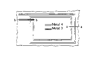
- Fig. 1 is a highly schematic, rectangular spiral layout as
seen from above for an integrated circuit inductor according to
state of the art,
- Fig. 2a and 2b are schematic cross secti O~A l views of the
inductor in fig. l,
- Fig. 3 is a schematic cross sectional view of an integrated
circuit inductor,
- Fig. 4 is a trench pattern to be used on a substrate,
- Fig. 5 shows a trench pattern under a metal conductor line.
DESCRIPTION OF A PREFERRED EMBODIMENT
In fig. 1 a state of the art rectangular spiral layout formi ng
an inductor is shown. The inductor is in this case formed in a
fourth, as counted bottom up, uppermost metal layer 101 by a
spiral, electrically conductive path comprising a number of
rectangular turns, the number of turns typically being between 5
and 10. A lower metallization layer 103, in this case the third
layer, is used for closing the spiral structure by means of a
cross-under.
The inductor structure of fig. 1 is also shown in cross section-
. ~
CA 022~6763 1998-11-30
W097/4S873 PCT/SE97/00954
al views in figs. 2a and 2b, the sections being taken along
lines a - a and b - b in fig. l, respectively. Thus, fig. 2a
shows the metal 201 of the fourth metal layer forming the rect-
angular turns. Underneath the metal spiral 201, there is an
oxide layer 203 applied to a silicon substrate 205. The thick-
ness of the metal layer is typically in the range of 1 - 2 ~m
and the thickness of the oxide layer is typically 6 ~m and the
width of the conductor paths can be about 5 ~m, the distance
between neighbouring paths being the same order of magnitude as
the width of the paths.
In fig. 2b, which is a cross sectional view along the line b - b
in fig. 1, also the third metal layer 207 is shown. The third
metal 207 layer constitutes a an electrically conductive cross-
under for completing the coil of the inductor. The fourth metal
layer 201 and the third metal layer are connected via electri-
cally conductive connectors 209. These connectors can be made in
a separate step using etching and metallization or, they can be
made by first making suitable holes and then filling the holes
with the material of the fourth layer.
Fig. 3 shows a cross sectional view of an inductor 305 having an
improved isolation, the inductor paths being formed in the top-
most, fourth metal layer on a silicon substrate 301. However,
before forming the structure on the silicon substrate 301, an
etching operation for producing a trench has been performed on
the silicon substrate 301 followed by a refilling of the
trenches with an isolating material, i.e. a material that has a
lower electrical conductivity than that of the substrate. The
refilled trenches 303 serve as to increase the effective
distance from the metal layer of the inductor to the semi-
conducting substrate. The losses in the substrate and the
capacitance to the substrate will then decrease. The Q-value and
the self-resonance frequency of the inductors will also increase
accordingly.
The trenches can be made substantially as in the recited con-
ventional methods used in modern IC processes for device
isolation. Deep and narrow trenches can thus be produced by dry
CA 022~6763 1998-11-30
W097/4S873 PCT/SE97/00954
etching and refilling the etched voids with an isolating
material like silicon oxide and undoped poly-silicon or a
dielectric material. The surface above the substrate produced in
the refilling process will then still be substantially flat. The
trench~s can have widths of about 1 - 2 ~m and depths of about 5
- 20 ~m. The width of the substrate material between neigh-
bouring trenches may be as small as is practically possible, for
instance 2 - 4 ~m. The trenches are arranged in some suitable
pattern to cross the overlying conductor paths.
Fig. 4 shows a view of a portion of a substrate 401 from above
in which a preferred pattern of trenches 403 has been etched.
The trench pattern is then used under an inductor for reducing
the losses to the substrate. The pattern comprises a first set
of several straight identical trenches located in parallel to
each other and having an equal spacing and also a second set of
identical trenches located in parallel to each other and equally
spaced, the trenches of the second set being perpendicular to
those of the first set. The tren~hes should always be so long
and located that they pass beyond the outermost inductor turn
into the free material surrolln~ing the inductor. The trench
pattern used can however have any meshlike shape, and it is
generally desirable to remove as much of the substrate as
possible.
Finally, fig. 5 shows how the method as described herein can be
used in another application. In this case trenches 501 are
etched under a metallization line 503 in order to reduce the
parasitic capacitance and reduce losses to the substrate. The
trenches may have the same dimensions as discussed above and
they are arranged to cross under the electrically conductive
path at substantially straight angles. They can be located
symmetrically under the conductor path and extend to each side
of the path as long as is required or possible, e.g. some 4 - 10
~m. This trench configuration or preferably the meshlike con-
figuration of fig. 3 can be also used for reducing losses of
bond pads.
,.. . .