Language selection

Search

Patent 2256926 Summary

Third-party information liability

Some of the information on this Web page has been provided by external sources. The Government of Canada is not responsible for the accuracy, reliability or currency of the information supplied by external sources. Users wishing to rely upon this information should consult directly with the source of the information. Content provided by external sources is not subject to official languages, privacy and accessibility requirements.

Claims and Abstract availability

Any discrepancies in the text and image of the Claims and Abstract are due to differing posting times. Text of the Claims and Abstract are posted:

  • At the time the application is open to public inspection;
  • At the time of issue of the patent (grant).
(12) Patent: (11) CA 2256926
(54) English Title: TUNABLE CHIRPED FIBER GRATING DEVICE AND METHOD FOR FORMING CHIRPED FIBER GRATING
(54) French Title: DISPOSITIF A RESEAU DE FIBRES COMPRIMEES ACCORDABLE ET METHODE DE FABRICATION DE RESEAU DE FIBRES COMPRIMEES
Status: Expired and beyond the Period of Reversal
Bibliographic Data
(51) International Patent Classification (IPC):
  • G02F 01/035 (2006.01)
  • G02F 01/01 (2006.01)
(72) Inventors :
  • PARK, MOO-YOUN (Republic of Korea)
(73) Owners :
  • SAMSUNG ELECTRONICS CO., LTD.
(71) Applicants :
  • SAMSUNG ELECTRONICS CO., LTD. (Republic of Korea)
(74) Agent: SMART & BIGGAR LP
(74) Associate agent:
(45) Issued: 2002-02-05
(22) Filed Date: 1998-12-23
(41) Open to Public Inspection: 1999-06-30
Examination requested: 1998-12-23
Availability of licence: N/A
Dedicated to the Public: N/A
(25) Language of filing: English

Patent Cooperation Treaty (PCT): No

(30) Application Priority Data:
Application No. Country/Territory Date
97-82102 (Republic of Korea) 1997-12-31

Abstracts

English Abstract


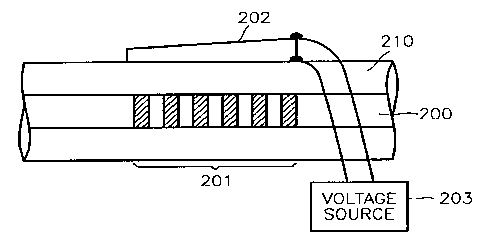
A tunable chirped grating device an optical fiber having the same spacings
between index perturbations, a piezoelectric element bonded to the optical fiber,
for changing the perturbation spacings according to an applied voltage, and a
voltage source for applying the voltage to the piezoelectric element. Since a
predetermined piezoelectric element is bonded to an optical fiber provided with a
grating having regular spacings and the perturbation spacings can be differentlydeformed by applying different electric field to respective perturbation positions by
the piezoelectric element, and the chirping rates of the reflected wavelengths
waves can be adjusted, a chirped grating device whose manufacturing procedure
is simple and which has flexibility can be provided.


Claims

Note: Claims are shown in the official language in which they were submitted.


CLAIMS:
1. A tunable chirped grating device comprising:
an optical fiber having equal spacings between index perturbations of a
chirped grating:
an elongated piezoelectric element having one end with a thickness greater
than an opposite end in the longitudinal direction, bonded to the optical
fiber, for
varying the spacings between the perturbations in response to an applied
voltage;
and
a voltage source for applying the voltage to the piezoelectric element.
2. The tunable chirped grating device as claimed in claim 1, wherein the
material of the piezoelectric element is Pb(Zr x Ti1-x)0 3.
3. The tunable chirped grating device as claimed in claim 1, wherein the
piezoelectric element is wedge-shaped and is bonded to the optical fiber using
an
epoxy.
4. A method for forming a chirped grating including the steps of:
forming a grating having regularly spaced perturbations in a core of an
optical fiber;
bonding a wedge-spaced piezoelectric device to said optical fiber adjacent
said grating; and
stretching said optical fiber by applying a controlled voltage to said wedge-
shaped piezoelectric device in order to vary the spacings between the
perturbations.
5. The method as claimed in claim 4, wherein said step of stretching applies
different tensions to said optical fiber according to a variation in thickness
of said
wedge-shaped piezoelectric device.
5

Description

Note: Descriptions are shown in the official language in which they were submitted.


CA 022~6926 l998-l2-23
TUNABLE CHIRPED FIBER GRATING DEVICE
AND METHOD FOR FORMING CHIRPED FIBER GRATING
BACKGROUND OF THE INVENTION
1. Field of the Invention
The present invention relates to a tunabie chirped fiber grating device in
which the spacings of perturbations in the index of refraction vary with a strain
which is produced by applying a voltage across a predetermined piezoelectric
element and a method for forming a chirped fiber grating.
2. Description of the Related Art
A chirped grating is designed to have different perturbation spacings or
different effective refractive indices depending on positions of the perturbations,
and is characterized in that the wavelength of reflected light differs depending on
the positions of the perturbations. FIGS. 1A and 1B show side views illustratingan optical fiber in which a chirped grating is formed. Here, a core is represented
by reference numeral 100 or 120, a cladding by 110 or 130, and a grating by 101
or 102. The chirped grating 101 in the core 100 according to FIG. 1A has a
structure in which the spacings of successive perturbations are different from each
other, while the effective refractive indices of the perturbations are the same, and
a chirped grating 102 in the core 120 according to FIG. 1B has a structure in
which the spacings of successive perturbations are the same, while the effectiverefractive indices of the perturbations are different from each other.
However, such chirped gratings are doomed to experience more
complicated procedures than those having equal perturbation spacings, and since
the chirping rates of the reflected wavelengths according to the positions of the
perturbations are fixed to values in fabrication conditions and therefore the
gratings can be used for a specific wavelength band, and the gratings cannot be
applied flexibly.
SUMMARY OF THE INVENTION

CA 022~6926 l998-l2-23
To solve the above problem, it is an objective of the present invention to
provide a tunable chirped grating device whose perturbation spacings differ fromeach other by attaching an element whose length can vary with an applied voltageto an optical fiber including a grating in which spacings between perturbations are
are regular and controlling the applied voltage, and a method for forming a chirped
fiber grating.
Accordingly, to achieve the above objective, there is provided a tunable
chirped grating device characterized in that the tunable chirped grating device
includes an optical fiber having the same spacings between index perturbations, a
piezoelectric element bonded to the optical fiber, for changing the perturbationspacings according to an applied voltage, and a voltage source for applying the
voltage to the piezoelectric element.
To achieve the above objective, there is provided a method for forming a
chirped fiber grating characterized in that the method includes the steps of (a)forming a grating having regularly spaced perturbations in the optical fiber, and (b)
causing the perturbation spacings of the optical fiber grating to differ from each
other by applying different tensions to the optical fiber grating according to the
positions of the perturbations.
BRIEF DESCRIPTION OF THE DRAWINGS
The above objective and advantages of the present invention will become
more apparent by describing in detail a preferred embodiment thereof with
reference to the attached drawings in which:
FIGS. 1A and 1B are side views illustrating an optical chirped grating is
formed; and
FIG. 2 is a side view illustrating the structure of a tunable chirped grating
device according to the present invention.
DESCRIPTION OF THE PREFERRED EMBODIMENTS
FIG. 2 shows a side view illustrating the structure of a tunable chirped
grating device according to the present invention. The tunable chirped grating
device shown in FIG. 2 includes an opticla fiber in which a grating 201 having

' CA 022~6926 l998-l2-23
.
perturbations which have the same refractive index perturbations and regularly
spaced therebetween in a core 200 formed inside a cladding 210, a piezoelectric
element 202 attached to the optical fiber, and a voltage source 203 for supplying a
voltage to the piezoelectric element 202.
A method for forming a chirped grating using the above described structure
is as follows. That is, the grating 201 having regularly spaced perturbations isformed in the optical fiber core 200, and the spacings of perturbations are caused
to differ from each other by applying different tensions to the optical fiber grating
201 according to the positions of the perturbations. The tensions are created bythe piezoelectric element 202 and the voltage source 203.
The grating 201 satisfies the following Bragg condition in the optical fiber
core 200.
~Ij = 2-n ffdj
where Aj is the wavelength of an incident wave, n ffiS the effective index of
refraction, and dj is the spacing between perturbations.
The material of the piezoelectric element 202 attached on the outside of the
grating 201 is a material which can be deformed according to the voltage appliedby the voltage source 203, and Pb(Zr Ti1 )o3. 0.4 ' x ' 0.6 (PZT or Lead
Zirconate Titanate) is preferably appropriate for the material. Epoxy may be used
as the adhesive. The piezoelectric element 202 made of a material such as PZT
deforms in a direction perpendicular to the applied electrical field. The shape of
the piezoelectric element 202 is preferably wedge-shaped in order for
deformations at each position to occur with different degrees from each other
according to the applied voltage. That is, though the applied voltage is constant,
as a portion of the piezoelectric element 202 is thicker, the electrical field becomes
relatively weaker than a thinner portion. As a result, the thinner portion deforms to
a smaller extent than the thicker portion.
The perturbation spacings of the grating 201 bonded to the piezoelectric
element 202 having the above-described characteristics vary with the deformationof the piezoelectric element 202. Consequently, a chirped grating device having

CA 022~6926 l998-l2-23
different spacings between perturbations can be formed. Further, when the
voltage applied by the voltage source 203 is adjusted, the chirping rates of thereflected wavelengths can be adjusted.
According to the present invention, since a predetermined piezoelectric
element is bonded to an optical fiber provided with a grating having regular
perturbation spacings and the perturbation spacings can be differently deformed
by applying different electrical fields to respective perturbation positions by the
piezoelectric element, and the chirping rates of the reflected wavelengths can be
adjusted, a chirped grating device whose manufacturing procedure is simple and
which has flexibility can be provided.

Representative Drawing
A single figure which represents the drawing illustrating the invention.
Administrative Status

2024-08-01:As part of the Next Generation Patents (NGP) transition, the Canadian Patents Database (CPD) now contains a more detailed Event History, which replicates the Event Log of our new back-office solution.

Please note that "Inactive:" events refers to events no longer in use in our new back-office solution.

For a clearer understanding of the status of the application/patent presented on this page, the site Disclaimer , as well as the definitions for Patent , Event History , Maintenance Fee  and Payment History  should be consulted.

Event History

Description Date
Time Limit for Reversal Expired 2007-12-24
Letter Sent 2006-12-27
Inactive: IPC from MCD 2006-03-12
Grant by Issuance 2002-02-05
Inactive: Cover page published 2002-02-04
Inactive: Final fee received 2001-10-25
Pre-grant 2001-10-25
Notice of Allowance is Issued 2001-09-19
Letter Sent 2001-09-19
Notice of Allowance is Issued 2001-09-19
Inactive: Approved for allowance (AFA) 2001-08-31
Amendment Received - Voluntary Amendment 2001-05-24
Inactive: S.30(2) Rules - Examiner requisition 2001-01-30
Inactive: Cover page published 1999-07-27
Application Published (Open to Public Inspection) 1999-06-30
Inactive: Single transfer 1999-03-22
Inactive: IPC assigned 1999-02-12
Classification Modified 1999-02-12
Inactive: First IPC assigned 1999-02-12
Inactive: Courtesy letter - Evidence 1999-02-02
Inactive: Filing certificate - RFE (English) 1999-01-28
Application Received - Regular National 1999-01-27
Request for Examination Requirements Determined Compliant 1998-12-23
All Requirements for Examination Determined Compliant 1998-12-23

Abandonment History

There is no abandonment history.

Maintenance Fee

The last payment was received on 2001-11-13

Note : If the full payment has not been received on or before the date indicated, a further fee may be required which may be one of the following

  • the reinstatement fee;
  • the late payment fee; or
  • additional fee to reverse deemed expiry.

Patent fees are adjusted on the 1st of January every year. The amounts above are the current amounts if received by December 31 of the current year.
Please refer to the CIPO Patent Fees web page to see all current fee amounts.

Fee History

Fee Type Anniversary Year Due Date Paid Date
Request for examination - standard 1998-12-23
Application fee - standard 1998-12-23
Registration of a document 1999-03-22
MF (application, 2nd anniv.) - standard 02 2000-12-25 2000-11-27
Final fee - standard 2001-10-25
MF (application, 3rd anniv.) - standard 03 2001-12-24 2001-11-13
MF (patent, 4th anniv.) - standard 2002-12-23 2002-11-19
MF (patent, 5th anniv.) - standard 2003-12-23 2003-11-17
MF (patent, 6th anniv.) - standard 2004-12-23 2004-11-08
MF (patent, 7th anniv.) - standard 2005-12-23 2005-11-08
Owners on Record

Note: Records showing the ownership history in alphabetical order.

Current Owners on Record
SAMSUNG ELECTRONICS CO., LTD.
Past Owners on Record
MOO-YOUN PARK
Past Owners that do not appear in the "Owners on Record" listing will appear in other documentation within the application.
Documents

To view selected files, please enter reCAPTCHA code :


To view images, click a link in the Document Description column (Temporarily unavailable). To download the documents, select one or more checkboxes in the first column and then click the "Download Selected in PDF format (Zip Archive)" or the "Download Selected as Single PDF" button.

List of published and non-published patent-specific documents on the CPD .

If you have any difficulty accessing content, you can call the Client Service Centre at 1-866-997-1936 or send them an e-mail at CIPO Client Service Centre.

({010=All Documents, 020=As Filed, 030=As Open to Public Inspection, 040=At Issuance, 050=Examination, 060=Incoming Correspondence, 070=Miscellaneous, 080=Outgoing Correspondence, 090=Payment})


Document
Description 
Date
(yyyy-mm-dd) 
Number of pages   Size of Image (KB) 
Claims 2001-05-23 1 34
Abstract 1998-12-22 1 21
Description 1998-12-22 4 162
Claims 1998-12-22 1 42
Drawings 1998-12-22 1 14
Representative drawing 2002-01-13 1 6
Representative drawing 1999-07-20 1 5
Filing Certificate (English) 1999-01-27 1 163
Courtesy - Certificate of registration (related document(s)) 1999-05-04 1 116
Reminder of maintenance fee due 2000-08-23 1 110
Commissioner's Notice - Application Found Allowable 2001-09-18 1 166
Maintenance Fee Notice 2007-02-06 1 171
Correspondence 2001-10-24 1 35
Correspondence 1999-02-01 1 31
Fees 2000-11-26 1 33
Fees 2001-11-12 1 32