Note: Descriptions are shown in the official language in which they were submitted.
CA 022~7639 1998-12-08
W O 98146050 PCT~B98/00416
TRlAC DIMMABLE COMPACT FLUORESCENT LAMP WITH LOW POWER FACTOR
This invention relates generally to a ballast for powering one or nore lamps,
C~ l iSil~g:
an input stage coupled to the mains;
an output stage co"ll)lising an inverter and coupled to the mput stage for
supplying power to the one or more lamps; and
a feedback circuit coupled between the output stage and the input stage for
feeding to the input stage a signal produced by the output stage and representative of the
voltage across the one or more lamps.
The invention also relates to a compact fluorescent lamp.
A conventional compact fluorescent lamp inrh~ c a ballast for powering the
lamp. The ballast is positioned subst~nti~lly within the lamp base. In order to meet
constrained space requirements, it is desirable to limit the number of ballast components
required for power factor correction. Without power factor correction, a compact fluorescent
lamp will operate at about a power factor of 0.5. There is also a growing demand for
compact fluorescent lamps which can dim, that is, which can adjust the level of light
produced by the lamp. Dimming of a compact fluorescent lamp controlled by a triac dirnmer
is highly desirable.
A compact fluorescent lamp with a power factor of about 0.5 essenti~lly draws
current in spikes from the A.C. mains, that is, each half cycle at about the line voltage peak.
No current is otherwise drawn from the A.C. mains during each half cycle. A triac dimmer,
however, cannot effectively dim a compact fluorescent lamp which draws current only in
spikes from the A.C. mains. Triac dimmers require a l~trhing current flowing therethrough
to be turned on and a holding current flowing ther~ ough to sustain conduction. Conse-
quently, a triac dimmer for controlling the light output of a compact fluorescent lamp having
a power factor of about 0.5 can be turned on only during the current spike and will imm~rli-
ately turn off after the current spike. For a triac dimmer to effectively control the light
output of a compact fluolescel" lamp, current should be drawn through the triac dimrner for
.
CA 022~7639 1998-12-08
W O ~8116~50 PCT~B98/00416
a s~bst~nti~l period of time during each half cycle of the A.C. mains. Current can be drawn
through the triac dimmer for a substantial period of time during each half cycle of the A.C.
mains by increasing the compact fluorcscellL lamp power factor. Compact fluorescent lamps
with high power factors, such as disclosed in U.S. Patent No. 5,313,142, provide fee~back
5 of a high frequency signal to the input of a ballast rectifier. As the power factor is increased
and especi~lly at power factors approaching 1.0, larger sized col."~ol1ents are required to
handle increased power levels. The larger sized components are diffirnlt to accommod~te in
a compact fluorescent lamp due to limited space requirements.
Accordingly, it is desirable to provide an improved triac ~limm~'nle compact
10 fluorescent lamp. The improved triac climm~hle compact fluorescent larnp should be at a low
power factor thereby ~ g the need for large sized components.
A ballast as described in the opening paragraph is therefore characterized in that
15 the output stage includes a voltage divider network having at least two components forming a
junction therebetween, respective ends of the voltage divider being connected to respective
terrninals of the inverter and the junction being connected to the fee-lback circuit.
The feeclb~rk circuit increases the current being drawn by the compact
fluorescent lamp during each half cycle of the A.C. mains. The voltage divider is so
~imrn~ioned that as compared to a conventional compact fluorescent lamp without power
factor correction, the ballast in accordance with the invention draws sufficient current from
the A.C. mains to permit dimminE control by a triac dimmer. Power factor correction
through the feedb~ck circuit, however, remains relatively low. Advantageously, the increase
in current dem~nll arising from the feedb~rk circuit can be met without a sllbs~nsi~l increase
in the area required for the ballast components within the standard compact fluorescel~L base.
Preferably the voltage divider network is in parallel with the one or more
larnps.
It is a feature of this first aspect of the invention that the input stage include a
voltage doubler and a rectifier. The output stage typically includes a lesonall~ tank circuit
formed, in part, from the at least two components. _
Alternatively the voltage divider in a ballast according to the invention can beso ~lim~n~ioned that the amount of power fed back by the feedh~k circuit is chosen such
CA 022~7639 1998-12-08
WO ~8146~50 PCTnB98/00416
that, for a particular lamp voltage of the one or more lamps, a relatively low amount of THD
is produced by the ballast and the power factor of the ballast is relatively high. In other
words the arnount of power fed back can be optimized for a range of values of the lamp
voltage so as to minimi7~ THD by means of tlim.oncioning of the voltage divider network.
Accordingly, it is an object if the invention to provide a ballasl having a voltage
divider and a feedb~ck circuit that generates a low amount of THD.
It is also an object of the invention to provide an improved triac dimm~hle
comr~ct fluorescent lamp with low power factor.
It is another object of the invention to provide an improved triac dimm~hle
10 compact fluorescent lamp having a fee-lb~ck circuit for increasing current demand.
It is further object of the invention to provide an improved triac rlimm~ le
fluorescent lamp which minimi7~c the need for large sized ballast components.
Still other objects and advantages of the invention, will, in part, be obvious and
will, in part, be ap~ale,ll from the specifir~tion.
For a fuller unde~ n~ g of the invention, reference is had to the following
description taken in connection with the accompanying drawings, in which:
FIG. 1 is a block diagram of a triac ~imm~hle compact fluorescent lamp in
20 accordance with the invention;
FIG. 2 is a sch~om~tir of a triac di~nrner as shown in FIG. l;
FIG. 3 is a sch~rn~tic of a compact fluorescent lamp;
FIG. 4 is a logic block diagram of an integrated circuit which serves as the
drive control circuit of FIG. 3; and
FIG. 5 is a sch~m~tic diagram of a Schmitt trigger shown in FIG 3.
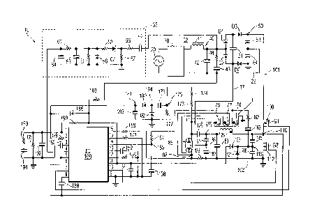
As shown in FIG. 1, a compact fluo~3cent lamp (CFL) 10 is supplied through
a triac dimmer 30 from an A.C. power line ~ rcs~ ed by an A.C. source 20. Compact
30 fluorescent lamp 10 in~lnrlec a d~mped electr-m~gnPtir hl~ relel~ce (EMI) filter 40, an
auxiliary power supply 45, a rectifier/voltage doubler 50, a ~1immin~ interface 55, an
inverter 60, a drive control circuit 65, a load 70 and a power fee~lb~k circuit 90. The output
of inverter 60, which serves as the output for the ballast of CFL lO, is connected to load 70.
Load 70 includes a lamp 85 and a l,,..ona"l tank circuit formed from a primary winding 75 of
CA 022~7639 1998-12-08
W O9~t~6~50 PCT~B98tO0416
a ~a.,srol",er T and a plurality of c~r~ritors 80, 81 and 82. The damped EMI filter 40
~ignifit~ntly dampens h~rmonirs (i.e. oscillations) generated by inverter 60. Rectifier/voltage
doubler 50 rectifies the sinusoidal voltage supplied by A.C. source 20 resulting in a D.C.
voltage with ripple which is boosted and made into a s~lbst~nti~lly constant D.C. voltage
S supplied to inverter 60. Those portions of compact fluorescent lamp 10 other than lamp load
70 are commonly grouped toge~1er and rel~ d to as fo",lillg a ballast for powering lamp
load 70.
Inverter 60 is driven by drive control circuit 65 at a varying switching
frequency based on the level of ill~ ion desired. The D.C. voltage is converted by
10 inverter 60 into a square wave voltage waveform applied to load 70. The level of lamp
illumination can be increased and decreased by decreasing and increasing the frequency of
this square wave voltage waveform, respectively.
The desired level of lamp illumination is set by triac dirnmer 30 and is
co--,l"l~ at~(l to drive control circuit 65 through a tlimming interface 55. Power feedback
15 circuit 90 feeds a portion of the power from the resonant tank circuit back IO the voltage
doubler resulting in only minim~l power factor correction being n.ocess~ry to sustain triac
conduction after firing. Auxiliary power supply 45 provides power to drive control 65 to
supplement the supply of power to drive control 65 when the rail voltage for inverter 60
momentarily drops in meeting load ~em~n~.
As shown in FIG. 2, triac dimmer 30 is connected across A.C. source 20
through a pair of lines 21 and 22. Triac dimmer 30 includes a capacitor 31 which is charged
through the serial combination of an inductor 32 and a variable resistor 33. A diac 34 is
connected to the gate of a triac 35. When the voltage on capacitor 31 reaches the voltage
breakdown of diac 34, triac 35 fires. Current (i.e. l~t~hing current of triac 35) is supplied to
25 CFL 10 through inductor 32 and triac 35. At the end of the 60 Hz, ~/2 wave cycle, the level
of current in triac 35 decreases below its holding current (i.e. minimllm anode current
n~cess~ry to sustain conduction of triac 35). Triac 35 turns off. The firing angle, that is, the
angle between 0 and 180 degrees at which triac 35 first conducts, can be adjusted by
c~nging the re~i~t~n~e of variable resistor 33. Variable resistor 33 can be, but is not limited
30 to, a potentiometer. The maximum firing angle is limited by the breakdown voltage of diac
34. Inductor 32 limits the rise or fall time of di/dt and thus protects triac 35 from a sudden
change in current. A c~racitor 36 serves as a snubber and prevents flicker especially when__~
the length of wiring b~l~eel~ triac 35 and CFL 10 is relatively long. Harmonics introduced
by the in~ ct~nce and parasitic capacitance ~oci~te(l with such long wiring are bypassed by
CA 022~7639 1998-12-08
W O9~ 50 PCT~B98/00416
s
c~r~ or 36. Consequently, the level of triac current and the operation of triac 36 are not
affected by the length of wiring between triac 35 and CFL 10. Flicker of lamp 85 through
such harmonics is avoided.
Triac dimmer 30 has two minimnm dim settings defined by/relative to CFL 10.
5 The first ...i~ -- dim setting (i.e. ~ -- turn on dim setting) is the lowest dim setting
possible to turn on lamp 85. The second miniml-m dim setting (i.e. minimllm steady state
dim setting), which is at a larger cut-in angle than the cut-in angle at the minimum turn on
dim setting, can be moved to after lamp 85 has reached its steady state operation. To ensure
flicker free operation, the power drawn by CFL 10 during preheat when at the minimllm turn
10 on dim setting must be greater than the power drawn during steady state operation at settings
between Illini-.,l--.- turn on and minimllm steady state. CFL 10 in combination with triac
dimrner 30 when at the minimllm turn on dim setting during preheat will draw more current
than after preheat whereby CFL 10 can complete preheat operation and operate in a steady
state mode.
As shown in FIG. 3, the damped EMI filter 40 includes an inductor 41, a pair
of capacitors 42 and 43 and a resistor 44. Resistor 44 and capacitor 43, which forrn a
snubber, are serially connected across the output of the damped EMI filter. This snubber
dampens oscillations produced by EMI filter 40 as triac 35 is turned on. These oscillations, if
not dampened by the snubber forrned by resistor 44 and capacitor 43, would decrease the
20 level of current flowing through triac 35 to below its holding current resulting in triac 35
being turned off. Resistor 44 and capacitor 43 also provide a path to avoid large dissipation
by filter 40 of 60 Hz power.
The rectifier and voltage doubler, which form a cascade half-wave voltage
doubler rectifier, includes a pair of diodes Dl and D2 and a pair of capacitors 53 and 54.
25 Diodes Dl and D2 rectify the sinusoidal voltage provided by damped EMI filter resulting in
a D.C. voltage with ripple. Capacitors 53 and 54 together serve as a buffer capacitor
boosting and making the rectified sinusoidal voltage into a s~hst~nti~lly constant D.C.
voltage supplied to inverter 60.
A c~pacitor 51 and a pair of diodes D3 and D4 provide a high frequency power
30 fee~lhacl~ signal from the fesonallL tank circuit to be further di.cc~ ed below. The high
frequency power feefl~cl~ signal switches diode D1 and a diode D3 between conductive and
non-conductive states during the positive half cycle of the 60 Hz waveform. Similarly, the_
high frequency power feedback signal switches diode D2 and a diode D4 between conductive
and non-conductive states during the negative half cycle of the 60 Hz waveform. The power
.
CA 022~7639 1998-12-08
W 0 98/46050 PCTnB98/00416
feedb~rk derived from the resol1dnt tank circuit (i.e. winding 75 and capacitors 80, 81 and
82) m~int~in~ the }evel of current through triac 35 above its holding current. Conduction of
triac 35 can be sl~c~in~d during a substantial portion of the 60 Hz, 1/2 cycle (i.e. about more
than 0.5 milli.cecond).
Dimming interface 55 provides an interface between the output of EMI filter 40
and drive control circuit 65. The angle at which triac 35 fires, that is, the cut in angle
~ Jles~ s the level of illllrnin~tic)n desired. Dimming interface 55 converts the cut-in angle
(i.e. tr~n~l~rçs the conduction pulse width of triac 35~ into a ~lo~ollional average rectified
voltage (i.e. ~limming signal) compatihle with and supplied to a DIM pin of an imegrated
10 circuit (IC 109) within drive control circuit 65.
Dimming interface 55 includes a plurality of resistors 56, 57, 58, 59 and 61;
capacitors 62, 63 and 64; a diode 66 and a zener diode 67. IC 109 is referenced to a circuit
ground. The voltage sampled by ~imming interface 55, which is supplied to the DIM pin of
IC 109, however, is shifted by a DC component. This DC component is equal to half the
15 buffer capacitor voltage of the voltage doubler, that is, the voltage across capacitor 54.
Capacitor 62 filters out this DC component. Capacitor 62 is also relatively large in size to
accommodate the line frequency. A pair of resistors 56 and 57 form a voltage divider which
together with a zener diode 67 determine the scaling factor which is applied in producing the
~limming signal. Resistors 56 and 57 also provide a discharge path for capacitor 62. The
20 average rectified voltage applied to the DIM pin is reduced by the zener voltage of zener
diode 67. Zener diode 67 therefore limits the maximum average rectified voltage (corres-
ponding to full light output) applied to the DIM pin. Variations in the maximum average
rectified voltage arising from differences in the minimllm cut-in angle of different triac
dimmers are limited by zener diode 67 to within a range of voltages which can be readily
25 i.l~ Led by IC 109. In other words, zener diode 67 establishes a ~ ll cut-in angle
(e.g. 25-30 degrees) co..~ ollding to a maximum level for the dimmin~ signal.
Zener diode 67 also limits the maximum firing (cut-in) angle of triac 35 during
the positive half cycle of the 60 Hz waveform (e.g. to about 150 degrees). The firing angle
is adjusted based on the values selected for resistors 56 and 57 and the breakdown voltage of
30 zener diode 67. Above a certain firing angle (e.g. above 150 degrees), the rail voltage of bus
101 is too low to develop a sufficient voltage at pin VDD to power IC 109. Inverter 60 is
th~ fole unable to operate and lamp 85 remains unlit.
Most triac dimmers have a mi.,i,.,u", firing (cut-in) angle of 25 to 30 degrees
which co.lc:s~,onds to full light output, At these small cut-in angles the maximum average
. CA 022~7639 1998-12-08
W O 98/46050 PCT~B98/00416
rectified voltage will be applied to a c~r~cieor 64. A plurality of resistors 56. 57, 58 and 59
and zener diode 67 inflllel-ce the dimming curve and in particular determine the maximum
firing angle at which lamp 85 provides full light output. That is, resistors 56, 57, 58 and 59
and zener diode 67 d~ llille the average rectified voltage which is sensed by the DIM pin
of IC 109 based on the firing angle of triac 35 chosen. The circuit for averaging the rectified
voltage is provided by resistor 61 and c~racitor 64. A c~raeit~-r 63 filters the high fre~uency
components of the signal applied to resistor 61 and c~r~ or 64.
During the negative half cycle of the 60 Hz waveform, a diode 66 limits the
negative voltage applied to the averaging circuit (resistor 61, c~raeitor 64) to a diode drop
(e.g. about 0.7volts). In an alternative embodiment, a zener diode 66' can be used in place
of diode 66 to improve regulation. Zener diode 66' will clamp the voltage applied to the
DIM pin such that the desired light level can be determined based on the duty cycle of the
voltage rather than on the average rectified voltage. For example, when the cut-in angle is
set to about 30 degrees for maximum light output of lamp 85, the duty cycle would
correspond to somewhat less than 50%. As the cut-in angle increases in order to decrease the
light output of lamp 85, the duty cycle would decrease.
Inverter 60 is configured as a half-bridge and includes a B+ (rail) bus 101, a
return bus 102 (i.e. circuit ground) a pair of switches (e.g. power MOSFETs) 100 and 112
which are serially connected between bus 101 and bus 102. Switches 100 and 112 are joined
together at a junction 110 and cornmonly identified as forrning a totem pole arrangement.
The MOSFETs serving as switches 100 and 112 have a pair of gates G1 and G2, respective-
ly. A pair of capacitors 115 and 118 are joined together at a junction 116 and serially
connPct~d between junction 110 and bus 102. A zener diode 121 is connected in parallel to
capacitor 118. A diode 123 is connected between a pin VDD of IC 109 and bus 102.Winding 75, c~racitor 80, a c~r~ritor 81, and a DC blocking capacitor 126 are
joined together at a junction 170. A pàir of secondary windings 76 and 77 of transformer T
are coupled to primary winding 75 for application of voltages across the filaments of lamp 85
in conditioning the latter during the preheat operation and when Ol.c.d~ g lamp load 85 at
less than full light output. C~ citQ~s 80, 82, 118, zener diode 121, switch 112 and a resistor
-30 153 are conn~ctPd together to a circuit ground. Lamp 85, resistor 153 and a resistor 168 are
joined together at a junction 88. A pair of resistors 173 and 174 are serially connected
between a junction 175 and the junction joining larnp 85 and c~pacilor 126 together.
Capacitors 81 and 82 are serially connrcted together and are joined at a junction 83.
C~raritor 51 of rectifier and voltage doubler 50 is co~ ec~ed to junction 83. A resistor 177 is
.. ...
CA 022~7639 1998-12-08
wO 98/16~0 pcT/ls98/oo4l6
cQnn~ctecl bc~cell node 175 and a circuit ground. A c~pacitor 179 is connected between
junction 175 and a junction 184. A diode 182 is connected between junction 184 and a circuit
ground. A diode 180 is connected between junction 184 and a junction 181. A ~Al~ac;lor 183
is cQ~nPcte(l between junction 181 and a circuit ground.
Drive control circuit 65 in~ es IC 109. IC 109 inrludes a plurality of pins. A
pin RIN~ is CQnn~Clrd to junction 185. A c~racit~r 158 is connPctPd between junction 185
and a circuit ground. A pair of re~ ol~ 161 and 162 and a c~r~itor 163 are serially
co~n~cted between junction 185 and junction 116. The input voltage at pin RIND reflects the
level of current flowing through winding 75. The current flowing through winding 75 is
obtained by first sampling the voltage across a secondary winding 78 of tran~rol,l.e. T. The
sampled voltage, which is proportional to the voltage across winding 75, is then integrated
by an integrator formed by resistor 161 and capacitor 158. The integrated sampled voltage
supplied to pin RIND is lcyiese~ tive of the current flowing through winding 75.Reconstructing the current flowing through winding 75 by first sampling and then hltcgldting
the voltage of winding 78 results in far less power losses than conventional sch~m~os (e.g.
sensing resistors) in sensing the current flow through the resonant inductor. It would also be
far more difficult to reconstruct the current flowing through winding 75 otherwise since this
current is split between lamp 85, resonant c~r~hors 80, 81 and 82 and a power feedb~ck
line 87.
VDD supplies the start-up voltage for driving IC 109 by connection to line 22
through a resistor 103. A pin LI1 is connected through a resistor 168 to junction 88. A pin
LI2 is connPcted through a resistor 171 to a circuit ground. The difference between the
~;u~el~ts inputted to pins LI1 and LI2 reflects the sensed current flowing through lamp 85.
The voltage at a pin VL, which is connected through a resistor 189 to junction 181, reflects
the peak voltage of larnp 85. The current flowing out of a CRECT pin into a circuit ground
through a parallel RC network of a resistor 195 and a c~racitcr 192 and the serial RC
network of a resistor 193 and a ~ r 194 reflects the average power of lamp 85 (i.e. the
product of lamp current and lamp voltage). An optional external D.C. offset, explained in
greater detail below, inrluti~s a serial combination of VDD and a resistor 199 which results
in a D.C. offset current flowing to a circuit ground through the resistor 195.
Capacitor 192 serves to provide a filtered D.C. voltage across resistor 195. A
resistor 156 is connlo-ct~rl between a pin RREF and a circuit ground and serves to set ~he
rc~lellcc current within IC 109. A c~p~cit()r 159, which is conn~oct~d between a CF pin and
a circuit ground, sets the fre~uency of a current controlled oscill~tor ~CCO) ~ cus~ed in
~ .
- CA 022~7639 1998-12-08
W O 9P'~6~eO PCT~B98/00416
greater detail below. A capacitor 165, which is connected between a pin and a circuit
ground, is employed for timing of both the preheat cycle and the non-oscillatinglstandby
mode as tli~c--~sed below. A GND pin is conn~cted directly to a circuit ground. A pair of
pins Gl and G2 are col~c~,led directly to gates Gl and G2 of switches 100 and 112,
S respectively. A pin Sl, which is conn~cted directly to junction 110, I'~ ,Scnl~ the voltage at
the source of switch 100. A pin FVDD is CQ~n.~~Clc'(lto junction 110 through a c~r~ciror 138
and feple~t~ the floating supply voltage for IC 109.
Operation of inverter 60 and drive control circuit 65 is as follows. Initially (i.e.
during startup), as capacitor 157 is charged based on the RC time constant of resistor 103
10 and capacitor 157, switches 100 and 112 are in noncon-1~lctinE and con~lcting states,
csl,e~;lively. The input current flowing into pin VDD of IC 109 is m~int~in.od at a low level
(less than 500 microarnp) during this startup phase. Capacitor 138, which is connected
between junction 110 and pin FVDD, charges to a relatively constant voltage equal to
approximately VDD and serves as the voltage supply for the drive circuit of switch 100.
15 When the voltage across cap 157 exceeds a voltage turnon threshold (e.g. 12 volts), IC 109
enters its operating (oscillating/switching) state with switches 100 and 112 each switching
back and forth between their con~ucting and noncon~lucting states at a frequency well above
the resonant frequency determined by winding 75 and c~p~citQrs 80, 81 and 82.
IC 109 initially enters a preheat cycle (i.e. preheat state) once inverter 60
20 begins oscillating. Junction 110 varies between about 0 volts and the voltage on bus 101
depending on the switching states of switches 100 and 112. Capacitors 115 and 118 serve to
slow down the rate of rise and fall of voltage at junction 110 thereby reducing switching
losses and the level of EMI generated by inverter 60. Zener diode 121 establishes a p~ ting
voltage at junction 116 which is applied to c~p~citor 157 by diode 123. . A relatively large
25 operating current of, for example, 10-lS milli~mps supplied to pin VDD of IC 109 results.
Capacitor 126 serves to bloclc the D.C. voltage co~ ,on~ from being applied to lamp 85.
During the preheat cycle lamp 85 is in a nonignited state, that is, no arc has
been established within larnp 85. The initial o~ela~ g frequency of IC 109, which is about
100 kHz, is set by resistor 156 and caraeitor 159 and the reverse diode condnctin~ times of
30 switches 100 and 112. IC 109 immPdi~tely reduces the Op~.dLillg frequency at a rate set
internal to the IC . The reduction in frequency continues until the peak voltage across the RC
h,le~;ld~ol forrned by resistor 161 and c~pacitor 158 as sensed at the RIND pin is equal to -~4
volts (i.e. the negative peak voltage equal to .4 volts). The switching frequency of switches
100 and 112 is regulated so as to m~int~in the sensed voltage by the RIND pin equal to -.4
CA 022~7639 1998-12-08
W O 98/46050 PCTnB98/00416
volts which results in a relative constant frequency of about 80-85 kHz (defined as the
preheat rle~lu~.lcy) at junction 110. A relatively cor~Lall~ RMS current flows through winding
7S which through coupling to windings 76 and 77 perrnits the fil~mPntc (i.e. cathodes) of
lamp 85 to be sufficiently preconditioned for subsequent ignition of larnp 85 and to m~int~in
5 long lamp life. The duration of the preheat cycle is set by c~p~c;lor 165. When the value of
c~ r;lor 165 is zero (i.e. open), there is effectively no prehP~;..g of the fil~mem~ res~llting
in an instant start operation of lamp 85.
At the end of the preheat operation, as determined by c~pacitor 165, pin VL
ac~ -m~os a low logic level. Pin VL is at a high logic level during preheat. IC 109 now starts
sweeping down from its switching frequency at preheat at a rate set internal to IC 109 toward
an unloaded resonant frequency (i.e. resonant frequency of winding 75 and capacitors 80, 81
and 82 prior to ignition of lamp 85-e.g. 60 kHz). As the switching frequency approaches the
resonant frequency, the voltage across lamp 85 rises rapidly (e.g. 600-800 volts peak) and is
generally sufficient to ignite lamp 85. Once larnp 85 is lit, the current flowing therethrough
rises from a few milli~mps to several hundred milli~mps. The current flowing through
resistor 153, which is equal to the lainp current, is sensed at pins LI1 and LI2 based on the
current difr~le~Lial therebetween as proportioned by ItSi~ 168 and 171, Ic;,~eclively. The
voltage of lamp 85, which is scaled by the voltage divider combination of resistors 173, 174
and 177, is detectçd by a peak to peak detector forrned from diodes and 182 and capacitor
183 resulting in a D.C. voltage, proportional to the peak to peak lamp voltage, at junction
181. The voltage at junction 181 is converted into a current by resistor 189 flowing into pin
VL.
The current flowing into pin VL is multiplied inside IC 109 with the differential
currents between pins LI1 and LI2 resulting in a rectified A.C. current fed out of pin
CRECT into the parallel RC network of capacitor 192 and resistor 195 and series RC
network of resistor 193 and c~p~ritQr 194. These parallel and series RC networks convert the
A.C. rectified current into a D.C. voltage which is proportional to the power of lamp 85.
The voltage at the CRECT pin is forced equal to the voltage at the DIM pin by a feedback
circuit/loop contained within IC 109. R~ tion of power cone--n-P~ by lamp 85 results.
The desired level of ill~ ion of lamp 85 is set by the voltage at the DIM
pin. The feedb~r~ loop inrludes a lamp voltage sensing circuit and a lamp current sensing
circuit rli~cu~ecl in greater detail below. The switching frequency of half-bridge inverter 60
is adjusted based on this fee~lbacl~ loop whereby the CRECT pin voltage is made equal to the
voltage at the DIM pin. The CRECT voltage varies between 0.5 and 2.9 volts. Whenever the
CA 022~7639 1998-12-08
WOgP~16~50 Pcr/Iss8/004l6
11
voltage at the DIM pin rises above 2.9 volts or falls below 0.5 volts, it is clarnped internally
to 2.9 volts or 0.5 volts, les~e~ ely. The signal provided at the DIM pin is generated
through phase angle dim ming in which a portion of the phase of the A.C. input line voltage
is cut off. The cut-in phase angle of the input line voltage is converted into a D.C. signal
5 through (3i"""i~-~ interface 55 which is applied to the DIM pin.
The voltage at the CRECT pin is zero when larnp 85 ignites. Ac lamp current
builds up, the current generated at the CRECT pin, which is plopo.lional to the product of
lamp voltage and larnp current, charges c~raritors 192 and 194. The switching frequency of
inverter 60 decreases or increases until the voltage at the CRECT pin is equal to the voltage
10 at the DIM pin. When the dim level is set to full (100 %) light output, capacitors 192 and
194 are ~ d to charge to 2.9 volts and thele~o.~ the CRECT pin voltage rises to 2.9
volts based on the feedback loop. During the rise in voltage, the feedb~ck loop, discussed in
greater detail below, is open. Once the CR~CT pin voltage is at about 2.9 vol~s, the
feedback loop closes. Similarly, when the dim level is set to ~ - light output,
15 capacitors 192 and 194 are permitted to charge to 0.5 volts and therefore the CRECT pin
voltage rises to 0.5 volts based on the fee~b~ck loop. Generally, 0.5 volts at the DIM pin
corresponds to 10% of full light output. For deep ~imming down to 1% of full light output,
external offset provided by resistor 199, which is otherwise not required can be employed
such that 0.5 volts at the DIM pin corresponds to 1% of full light output. When the dim
level is set to the miniml-m light output, the CRECT capacitor charges to 0.5 volts before the
feedb~c~ loop closes.
Conventional lamps which are set to dim upon ignition typically exhibit an
ignition flash. The flash of light, which is above the level of illtlmin~tion desired, is
produced by supplying a high level of power to the lamp for a relatively long and
25 unn~cess~ry period after ignition (e.g. up to a few seconds). In this way, conventional
compact fluorescent lamp ignition schPm~s ensure succecsful ignition of the lamp. In
accordance with the invention, however, ignition flashes are minimi7.e~1. The duration of a
high light condition following ignition is very short for low dim settings and the visual
impact of the undesired light flash is .~ .od. Sul ~ avoidance of ignition flashes is
30 achieved by recl~cing the power level supplied to lamp 85 imm~ tPly after ignition takes
place through use of the feed~ loop.
In ~m~lg~m lamps, the lamp voltage drops sl~kst~nti~lly when the :~m~lg~m
le~ )e~alulc exceeds a predetermined level. The mercury vapor ples~.u~ is reduced causing
the lamp voltage to drop. Under such conditions, regulation of lamp power will result in
CA 022~7639 l998-l2-08
W O 98/46050 PCTnB98/00416
12
extremely high larnp cu,re~ and consequential destruction of the larnp electrodes and
shortening of lamp life.
In acco~ ce with the invention, an accepLable level of lamp current is
m~int~inPd by clamping the minimnm voltage at junction 181 equal to the VDD pin voltage
less the voltage drop of a diode 186. The voltage of lamp 85, which is scaled by the voltage
divider combination of resistors 173, 174 and 177, is ~letec~e~i by a peak to peak detector
formed from diodes and 182 and capacitor 183 resulting in a D.C. voltage, proportional to
the peak lamp voltage, at junction 181.
The voltage at junction 181, which is converted into a current by resistor 189
flowing into pin VL, is m~int~in~d equal to no less than the VDD pin voltage less the voltage
drop of diode 186. Since IC 109 regulates lamp power and by cl~ll~ing sampled lamp
voltage to a minimum value, the larnp current is limited to an acceptable maximum level.
An auxiliary power supply, which is formed by secondary winding 78 of
transro,l,lc, T, resistor 162 and capacitor 163, is provided to avoid flicker. Flicker is caused
by IC 109 turning off momentarily due to the voltage level at pin VDD falling below a
~--i-~i,.---.-, threshold required to power IC 109. As lamp 85 is turning on, CFL 10 draws
more current which can cause the voltage supplied by bus 101 to mom~orlt~rily dip. Since the
voltage at pin VDDis based on the voltage supplied by bus 101, a momentary reduction in
the voltage level at pin VDD below this minimnm threshold will result in flicker.
The auxiliary power supply supplements the main power supply. The main
power supply, established by zener diode 121, provides a pulsating voltage to capacitor 157
in charging the latter. The VDD pin voltage is set by and equal to the voltage across
capacitor 157. The auxiliary power supply provides a rectified voltage, after but not during
preheat, which is applied to pin VDD by coupling the voltage across winding 78 through
resistor 162, c~p~ritor 163 and diode 123. The auxiliary power supply provides a DC offset
to pin VDD which ensures that the voltage at pin VDDis m~int~in~d above a miniml~m
threshold of about 10 volts to power IC 109. The mom~nt~ry h.~e."l~Lion of light produced
by lamp 85 (i.e. flicker) due to the increased load as larnp 85is turning on is thereby
avoided.
Power is fedback to rectifier/voltage doubler 50 along power feedha~k line 87
from junction 83 to the junction joining diodes D2 and D4 and c~racitor 51 together. In
order to lower the overboost voltage supplied by rectifier/voltage doubler 50 to lamp 85 and~
increase the amount of current during ignition and ~limming conditions, the c~raçit~n~e
represented by c~racitors 81 and 82 of the resonant tank circuit has been split therebetween.
CA 022~7639 1998-12-08
WO ~8/160FO PCMB98/00416
13
Fee-lh~el~ current flows only through c~p~ritor 81 and ~lepen~lc on the ratio of c~pacit- r 81 to
c~r~citor 82. The ratio of c~racitQr 81 to c~pacil.Jr 82 depends on the ratio of lamp voltage
(i.e. voltage across larnp 85) to the line voltage (i.e. voltage of A.C. source 20).
Diodes D1 and D3 con~ ct when the line voltage is positive. Diodes D2 and D4
5 conduct when the line voltage is negative. During the peak portion of each half cycle of the
mains line voltage (i.e. voltage from A.C. source 20), there is no high frequency feedb~c~
contribution from c~pacitc-r 81. That is, the voltage during the peak portion of each half
cycle of the mains line is greater than the voltage at junction 83 such that the high frequency
contribution fed into rectifier/voltage doubler 50 is blocked by diodes D2 and D4.
C~r~ritor 51 is a D.C. blocking c~pacitor which electrically connects the
junction 3Oining diodes Dl and D3 to the junction joining diodes D2 and D4 with respect to
the high frequency feeclb~ck contribution from capacitor 81. Capacitor 51 thereby ensures
that the high frequency feedback contribution is the same (i.e. symmetrical) for both the
positive and negative half cycles of the mains line voltage. The amount of feedhac~ varies
15 based on the mains line voltage and dim setting. C~ra~itors 81 and 82 are effectively in
parallel with lamp 85 with respect to the high frequency power being fed back torectifier/voltage doubler 50. The power being fed back to rectifier/voltage doubler 50 reflects
the voltage across lamp 85.
The power feedback circuit advantageously permits CFL 10 to operate at a
20 power factor far less than 1.0 (e.g. about 0.7). When the power factor is about 1.0, there is
far greater stress on the components within inverter 60 and load 70 than at a lower power
factor. The power feedback circuit raises the power factor sufficiently to the minim~l level of
about 0.7 n.ocess~ry to sustain conduction of triac 35.
Turning now to FIG. 4, IC 109 in~ludes a power regulation and ~imming
25 control circuit 250. The diff~le.llial current b~.~een pins LI1 and LI2 is supplied to an active
rectifier 300. Active rectifier 300 full wave rectifies the A.C. waveforrn by employing an
arnplifier with internal feedb~c~ rather than a diode bridge to avoid any voltage drop
nn~ ly a~sori~tecl with diodes. A current source 303 in ,~ onse to the output of active
l~,lir.e~ 300 ge.le.~les a rectified current ILDIFF ~ lesel~l;ng the flow of current through
30 lamp 85 which is supplied as one of two inputs to a current multiplier 306.
A P channel MOSFET 331 is turned on and an N-channel MOSFET 332 is
turned off during preheat so as to pull the VL pin up to the voltage potential of pin VDD. At
the end of preheat cycle (e.g. 1 second in duration), P channel MOSFET 331 is turned off
and N channel MOSFET 332 is turned on to permit power regulation and dim control
_ _ . . . ...
CA 022~7639 l998-l2-08
WO 9~16~50 PCT~B98/00416
14
operation of inverter 60 to take place. Current following the preheat cycle flows through the
VL pin and N ch~nn~l MOSFET 332 and is scaled by a resistor 333. A current source (i.e.
current amplifier) 336 in resl,onse to the scaled current from the VL pin produces a current
signal IVL. A current clamp 339 limits the maximum level of current signal IVL which is
S fed into the other input of multiplier 306. A current source 309 outputs a current ICRECT in
response to the output of mull;plier 306 which is fed into both the CRECT pin and the
noninverting input of an error amplifier 312. As shown in FIG. 3, the parallel network of
capacitor 192 and resistor 195 in parallel with the series combination of resistor 193 and
capacitor 194 converts the A.C. rectified current at the CRECT pin into a D.C. voltage.
Referring once again to FIG. 4, a D.C. voltage at the DIM pin is applied to a
voltage clarnp circuit 315. Voltage clamp circuit 315 limits the voltage at the CRECT pin
between 0.3 and 3.0 volts. The output of voltage clamp circuit 315 is supplied to the
inverting input of error amplifier 312. The output of the error amp 312 controls the level of
current IDIF flowing through a current source 345. A current cu~llpaldlor 348 colll~,ares
15 current IDIF with a reference current IMIN and a current IMOD and outputs the current
signal of greatest m~gnitu~e. The IMOD current is controlled by a switch capacitor
integrator 327. The current ouL~ul~ed by current colllpdldtor 348 provides a control signal
which determines the osci}lation (switching) frequency at which VCO 318 oscillates. When
the lamp ignites, the CRECT pin voltage and IDIF current are zero. The output of the
20 co~ )al~lor 348 selects the maximum current level from among IMIN, IDIF and IMOD
which is IMOD. As the CRECT pin voltage builds up to the voltage at the DIM pin, the
IDIF current increases. When the IDIF current exceeds the IMOD current, the output of
colllpal~lor 348 is equal to the IDIF current.
The feedb~rl~ loop is centered about error amplifier 312 and includes many
25 components internal and external to IC 109 in making the voltage at the CRECT pin equal to
the voltage at the DIM pin. When the voltage at the DIM pin is below .3 volts, a D.C.
voltage of 0.3 volts is applied to the inverting input of error amplifier 312. When the voltage
at the DIM pin exceeds 3.0 volts, 3.0 volts is applied to error amplifier 312. The voltage
applied to the DIM pin should range from and inrhl~ling 0.3 volts to and inrl~ ing 3.0 volts
to achieve a desired ratio of 10:1 between the maximum and ~-.i-.;,.,.. light levels of lamp
85. Input to multiplier 306 is cl~mpecl by current clamp 339 to provide proper scaling of the
current into multiplier 306.
The frequency of CCO 318 in le~OnSe to the output of col"~ tor 348
controls the switching frequency of half bridge inverter 60. C~ paldtor 348 supplies the
CA 022~7639 1998-12-08
W O gP'-6~'0 PCT~B98/00416
IMOD current to CCO 318 during preheat and ignition sweep. Co~ uator 348 outputs to
CCO 318 the IDIF current during steady state operation. CCO 318 in response to the IMIN
current when uul~ull~d by co"ll.aralor 348 limits the ...;,.i-..~-- switching frequency The
",;j~j"~l,." switching frequency is also based on r~ o~ 159 and resistor 156 which are
S co~ r~(ed external to IC 109 at pins CF and RREF"~ e~Li~ely. Inverter 60 reaches close~d
loop operation when the CRECT pin voltage is at the same voltage as the DIM pin voltage.
Error amplifier 312 adjusts the IDIF current o~ u~l~d by con,l)alatol 348 so as to m~int~in
the C~ECT pin voltage about equal to the DIM pin voltage.
A resonant inductor current sense circuit monitors the currenl of the resonallt
10 inductor, as lep~esented by the signal at the RIND pin, in deterrnining whether inverter 60 is
in or near the capacitive mode of operation. Inverter 60 is in the capacitive mode of
operation when the current flowing through winding 75 leads the voltage across switch 112.
In the near capacitive mode of operation, the current flowing through winding 75 is close to
but does not yet lead the voltage across switch 112. For example, given a resonant frequency
15 based on winding 75 and capacitors 80, 81 and 82 of about 50 kHz, a near capacitive mode
of operation exists when the current flowing through winding 75 lags behind but is within
about 1 microsecond of the voltage across switch 112.
Circuit 364 also detects whether forward conduction or body diode conduction
(from the substrate to the drain) of switch 100 or 110 takes place. A signal IZEROb
20 produced by lesona,l~ inductor current sense circuit 364, that is, signal IZEROb produced at
the Q output of a flip-flop 370 is at a high logic level when either switch 100 or 112 is in
forward conduction and at a low logic level when the body diode of switch 100 or 112
conducts. Signal IZEROb is supplied to an IZEROb pin of CCO 318. When signal IZEROb
is at a low logic level, the waveform at the CF pin 379 is subst~n~ y at a constant level.
25 When signal IZEROb is at a high logic level and switch 100 is con(l~lcting, the voltage at the
CF pin is rising. When signal IZEROb is at a high logic level and the switch 112 is
com~ucting, the voltage at the CF pin is decreasinglfalling.
A signal CM produced by reson~lL inf~ tc)r current sense circuit 364, that is,
signal CM produced by an OR gate 373 is at a high logic level when the switching frequency
30 of inverter 60 is in the near capacitive mode of operation. A switch c~pacitor integrator 327
based on signal CM being at a high logic level will cause an increase in the output of current
source 329 (i.e. IMOD current). The increase in m~g~ de of the IMOD current results in_.
col~lpalalor 348 supplying the IMOD current to VCO 318 whereby an increase in the
~wilcllillg frequency of inverter 60 takes place. The near ca~,a.;ili~e mode of operation is
CA 022~7639 1998-12-08
W 0 98/~6CFO PCT~B98tO0416
16
~.e~cted by res~ h~.luclol current sense circuit 364 by monilolil1g the sign (+ or -) of the
voltage waveform at the RIND pin during the leading (rising) edge of each gate drive pulse
produced at pin Gl and G2 of IC 109. When the sign of the voltage waveforn at the RIND
pin during the leading edge of gate pulse Gl is + (positive) or of gate pulse G2 is -
(negative), inverter 60 is in a near capacitive mode of operation.
ANAND gate 376 outputs a CMPANIC signal which is at a h;gh logic level
when inverter 60 is opc.~ g in the capacitive mode. Once the c~acilive mode is detected,
the level of the IMOD current rapidly rises in response to the rapid rise in the output of
switch c~p~citor integrator 327. VCO 318 based on the IMOD signal, resistor 156 and
10 c~raciror 159 controls a relatively inct~nt~nPous rise to the maximum switching frequency of
inverter 60. The capacitive mode is detectecl by monitoring the sign (+ -) of the voltage
waveforrn at the RIND pin during the trailing (falling) edge of each gate drive pulse
produced at pin G1 and G2 of IC 109. When the sign of the voltage waveform at the RIND
pin during the trailing edge of gate pulse G1 is - (negative) or of gate pulse G2 is +
15 (positive), inverter 60 is in a capacili~e mode of operation.
A circuit 379 in le~.~onse to the value of c~paritor 165 (connected between pin
CP and a circuit ground) sets the times for pr~h~ting the fil~m~ntc of lamp 85 and for
placing inverter 60 into a standby mode of operation. During the preheat cycle, 2 pulses
(over a 1 second duration~ are generated at the CP pin. The switching frequency of inverter
20 60 during the preheat cycle is about 80 kHz. At the end of the preheat cycle, a signal IGNST
mçs a high logic level initi~ting an ignition start, that is, an ignition sweep in the
switching frequency from about 80 IcHz to about but above the resonant frequency of
winding 75 and capacitors 80, 81 and 82 of, for example, about 60 'kHz (unloaded ~cs(jnalll
frequency). The ignition sweep can be at a rate, for example, of 10 kHz/milliceconds.
IC 109 regulates the amplitude of current flowing through resonant winding 75
which is sensed at the RIND pin. When the voltage m~gnitll~e at the RIND pin exceeds .4, a
signal PC outputted by a coll,~lalor 448 acs~mPs a high logic level causing the output of
switch c~p~ or integrator 327 to adjust the level of the IMOD current. An inclease in the
RMS switching frequency results which reduces the arnplitude of the current flowing through
30 resol1al~l winding 75. When the voltage m~gnit~ e at the RIND pin falls below .4, signal PC
aCs~lmPs a low logic level causing the output of switch c~r~itor integrator 327 to adjust the
level of the IMOD signal such that the switching frequency decreases. An increase in the _.
current flowing through resonanl winding 75 results. A well regulated flow of current
through re30l1al~l winding 75 is achieved which permits a subst~n~ y consl~l,l voltage across
CA 022~7639 1998-12-08
WO ~8M~'0 PcTtlss8/004l6
17
each fil~m~nt of lamp 85 during preheat. Alternatively, by inrl~ ing a capacitor (not shown)
in series with each fil~m~nt a s~1bst~nti~lly constant current flow through the filaments can be
achieved during preheat.
Circuit 379 also inrl~ s an ignition timer which is initi~t~d following elapse of
the preheat cycle. Once activated, 1 pulse is gene~dted at the CP pin. If after this pulse either
a c~r~citive mode of inverter operation or an overvoltage condition across lamp 85 is
~etecte~l, IC 109 enters a standby mode of operation. During standby, VCO 318 stops
oscill~ting with switches 112 and 100 being m~int~int~ci in conductive and nonconductive
states, respectively. To exit the standby mode of operation, the supply voltage to IC 109 (i.e.
10 supplied to pin VDD) must be reduced to at least or below a turnoff threshold (e.g. 10 volts)
and then increased to at least a turnon threshold (e.g. 12 volts).
The preheat timer includes a Schmitt trigger 400 (i.e. a comparator with
hysteresis) which sets the tripping points of the CP waveform. These tripping points
represent the voltages applied to the input of the Schmitt trigger 400 for triggering the latter
15 on and off. A switch 403 when in a conductive state provides a path for discharge of
capacitor 165. Switch 403 is placed in a conductive state whenever and for the duration of
each pulse generated by Schrnitt trigger 400. Capaci~or 165 discharges whenever the voltage
at the CP pin exceeds the upper tripping point as established by Schmitt trigger 400. The
discharge path includes the CP pin, switch 403 and a circuit ground. Capacitor 165 is
20 charged by a current source 388. When a capacitive mode of operation is detected as
reflected by the generation of a CMPANIC signal at a NAND gate 376, a switch 392 is
turned on. Capacitor 165 is now also charged by a current source 391. Current charging
capacitor 165 is 10 times higher when the capacili~e mode of operation is detected. The
voltage at the CP pin reaches the upper tripping point of Schmitt trigger 400 in 1/10 the time
25 it takes when not in the capacitive mode. The pulse therefore at the CP pin is 10 times
shorter when the capacitive mode of operation is detectç(1 than when the capacitive mode of
operation is not ~etected. Consequently, IC 109 will enter the standby mode of operation in a
relatively short period of time whenever an hlLl~ase in the switching frequency does not
elimin~te the capacitive mode condition.
The preheat tirner also inrl~des a D-type flip flop forming counter 397. The
output of a NAND gate 406 generates a signal COUNT 8b which ~ ..es a low logic level
at the end of the ignition period. A gate 412 outputs a high logic level whenever an
overvoltage ...;.-i...i..~ threshold condition (i.e. as rep,esenled by the OVCLK signal) across
lamp 85 or a capacitive mode of inverter operation (i.e. as represented by signal CMPANIC)
CA 022~7639 l998-l2-08
W 098l46050 PCTnB98/00416
18
has been detected When the output of a gate 415 ~s~lm~s a high logic level, switch 403 is
turned on reS~lltin~ in the discharge of capacitor 165.
As ~iscllcsed above, following the preheat cycle the input current flowing from
the VL pin is fed to multiplier 306 through current source 336 for purposes of power
regulation and 11imming control. The input current from the VL pin also feeds the
noninverting inputs of a co~ tor 421, 424 and 427 through a current source 417, a
current source 418 and a current source 419, respectively.
Colllpar~Lor 421 in response to cle~ectinE that the lamp voltage has exceeded anovervoltage "~i";",~-" threshold activates the ignition timer. When the overvoltage minim-lm
10 threshold condition exists following elapse of the ignition timer, IC 109 enters the standby
mode of operation. A D type flip-~lop 430 clocks the output of co.lll)alator 421 at the falling
edge of the gate pulse produced at pin G2. The logic combination of a D-type flip-flop 433,
an AND gate 436 and a NOR gate 439 cause a switch (an N-channel MOSFET) 440 to open
and thereby block the ICRECT signal whenever the overvoltage minimnm threshold is
15 exceeded during the first ignition sweep. The flip-flop 433 has its D input tied to an internal
node 385. The D input of flip-flop 433 ~c~nmps a high logic level at the end of the preheat
cycle when an overvoltage minimnm condition is detectecl. The output of flip-flop 433 in
response to the high logic level at its D input ~c~nm~s a low logic level resulting in the
output of gate 439 switching to a low logic level. Switch 440 opens thereby blocking the
20 ICRECT signal from reaching the CRECT pin. When the ICRECT signal is blocked from
reaching the CRECT pin, capacitor 192 discharges through resistor 195. Full discharge
occurs if external offset 198 is not used. Partial discharge occurs when offset 198 is used as
shown in FIG. 2. In either event, discharge of c~paritor 192 lowers the voltage at the
CRECT pin to ensure that the feedb~r~ loop does not close. During the preheat cycle, the
25 IGNST signal at internal node 385 is at a low logic level. NOR gate 439 will therefore turn
off switch 440 during the preheat cycle. No ICRECT signal will be applied to error amplifier
312 or flow out of the CRECT pin so as to charge c~pacitor 192.
Once ignition sweep begins, which im m.of~i~t~ly follows completion of the
preheat cycle, the IGNST signal is at a high logic level. Switch 440 will now turn on and
30 remain turned on during ignition sweep unless a overvoltage ..,;~ .. threshold (e.g. about
l/2 the m~imllm voltage which will be applied to lamp 85 during ignition) is det~octPd by
co~ alator 421. During ignition sweep, the switching fre~uency is decl~asil1g resulting in an
increase in voltage across lamp 85 and sensed lamp current. The m~Enitu~e of the ICRECT
signal increases which charges capacitor 192 resulting in an increase in the voltage at the
CA 022~7639 1998-12-08
W O ~8/~50 PCTnB98/004~6
19
CRECT pin. At low dirn levels, the voltage at the CRECT pin could equal the voltage at the
DIM pin. Without further intervention, error arnplifier 312 det~cting no difference between
these two voltages will prematurely close the feedb~c~ loop prior to successful ignition of
larnp 85.
To avoid the premature closure of the fee(lbar~ loop, gate 439 during ignition
sweep will turn off switch 44G and m~int~in switch 440 turned off for as long as an
overvoltage miniml~m threshold condition exists as detected by colllpala~or 421. By blocking
the ICRECT signal from reaching the CRECT pin, the CRECT pin voltage drops and is
thereby prevented from equaling the DIM pin voltage even when the latter is set to a deep
10 dirn level. Accordingly, the feedb~c~ loop cannot close during ignition sweep and thereby
cannot prevent successful ignition from taking place. Preferably, switch 440 is turned off
only once during ignition sweep beginning when the larnp voltage reaches the overvoltage
minimum threshold and continllin~ until larnp 85 ignites. While switch 440 is ~urned off,
capacitor 192 can sufficiently discharge through resistor 195 to ensure that the feedback loop
15 will not prematurely close during ignition sweep.
Conventional compact fluorescent lamp driving schemes in order to provide for
successful lamp start-up supply a relatively high level of power to the lamp for an undesira-
bly long period of time (e.g. up to several seconds). When attempting to start a lamp at a
relatively low level of bri&hrn~ss, the undesirably long period of time at which the relatively
20 high level of power is supplied to the lamp can result in a condition referred lO as ignition
flash. Under this condition, a momentary flash of light, potentially far brighter than desired,
occurs.
In accordance with the invention, ignition flash has been substantially
elimin~t~d, that is, has been so minimi7~d as to not be noticed. Sl~hst~nti~l elimin~tion of
25 ignition flash has been achieved by avoiding the undesirably long period of time at which the
relatively high level of power is supplied to lamp 85. More particularly, lamp 85 is supplied
with a relatively high level of power for about 1 milli~econd or less before being reduced in
m~gnitnde following larnp ignition. This imm~ t~o reduction in lamp power is achieved by
monitoring overvoltage conditions and particularly when the lamp voltage drops below the
3~ overvoltage ~"il-i...,.", threshold (as deterrnined by co,~ tor 421) before permitting switch
440 to close again. This drop in lamp power below the overvoltage Illil.;llllllll threshold
occurs imm~ ely upon sn~ce~sful ignition of larnp 85. In other words, at s~lbst~nti~l _
li.lllll;llg levels where ignition flash can occur, the latter is avoided by first detecting when
the larnp voltage has been reached and/or exceeded the overvoltage minim~lm threshold and
....
subsequent thereto when the lamp voltage has dropped below the overvoltage minimum
threshold.
The output of comparator 424 assumes a high logic level when the lamp voltage
exceeds the overvoltage maximum threshold (e.g. two times the overvoltage minimum
threshold). When the output of comparator 424 is at a high logic level without detection of
the near capacitive mode, switch capacitor integrator 327 increases the oscillating frequency
of VCO 318 and therefore the switching frequency at a fixed rate (e.g. at a sweep rate of 10
kHz/millisec) based on the Q output of a D-type flip-flop 445 assuming a high logic level
(i.e. signal FI (frequency increase) outputted by flip-flop 445 being at a high logic level).
The time interval of the switching period of inverter 60 is therefore reduced. When the
output of comparator 424 is at a high logic level and a near capacitive condition is detected,
switch capacitor integrator 327 increases the oscillating frequency of VCO 318 and therefore
the switching frequency immediately (e.g. within 10 microseconds) to its maximum value
(e.g. 100 kHz) based on the output of a NAND gate 442 assuming a high logic level (i.e.
signal FSTEP (frequency step) outputted by NAND gate 442 assuming at a high logic level).
The switching period of inverter 60 is reduced to its minimum time interval (e.g. 10
microseconds) in response to VCO 318 now at its maximum oscillating value.
The output of comparator 427 assumes a high logic level when the lamp voltage
exceeds an overvoltage panic threshold (i.e. above the overvoltage maximum threshold).
When the output of comparator 427 is at a high logic level, switch capacitor integrator 327
increases the switching frequency of VCO 318 immediately to its maximum value based on
the output of a NAND gate 442 assuming a high logic level (i.e. signal FSTEP (frequency
step) outputted by NAND gate 442 assuming a high logic level).
Gate driving circuit 320 is well known in the art and is more fully described inU.S. Patent No. 5,373,435. The description of the gate driving circuit in U.S. Patent No.
5,373,435 is incorporated herein by reference thereto. Pins FVDD, G1, S1 and G2 of IC 109
correspond to nodes PI, P2, P3 and GL as shown in FIG.1 of U.S. Patent No.5,373,435.
Signals G1L and G2L shown in FIG. 3 herein correspond to the signals at terminal 1N L and
between a controller and level shifter when the upper drive DU is on in U.S. Patent No.
5,373,435, respectively.
A supply regulator 592 includes a bandgap regulator 595 which generates an
output voltage of about 5 volts. Regulator 595 is substantially independent over a wide range
of temperatures and supply voltage (VDD). The output of a Schmitt trigger (i.e. comparator
with hysteresis) 598, referred to as the LSOUT (low supply out) signal, identifies the
CA 022~7639 1998-12-08
W O 9P'46~S0 PCT~B98/00416
21
condition of the supply voltage. When the input supply voltage at the VDD pin exceeds a
turnon threshold (e.g. I2 volts), the LSOUT signal is at a low logic level. When the input
supply voltage at the VDD pin falls below a turn-off threshold (e.g. 10 volts), the LSOUT
signal is at a high logic level. During startup, the LSOUT signal is at a high logic level
~ 5 which sets the output of a latch 601, referred to as a STOPOSC signal, to high logic level.
VCO 318 in response to the STOPOSC signal a~ ..,i..g a high logic level st~ps VCO 318
from oscillating and sets the CF pin equal to the output voltage of bandgap regulator 595.
When the supply voltage at the VDD pin exceeds the turnon threshold resulting
in the LSOUT signal ac~l~ming a low logic level, the STOPOSC signal assumes a low logic
level. VCO 318 in response to the STOPOSC signal being at a low logic level will drive
inverter 60 so as to oscillate at a switching frequency as described herein with a subst~nti:~lly
trapezoidal waveform being applied to the CF pin. Whenever the VDD pin voltage drops
below the turnoff threshold and the gate drive at pin G2 assumes a high logic level, VCO
318 stops oscillating. Switches 100 and 112 will be m~int~in~d in their nonconductive and
conductive states, respectively.
The output of latch 601 also ~ssumes a high logic level resulting in VCO 318
stopping to oscillate and assuming a standby mode of operation whenever the output of a
NOR gate 604 ~s~mPc a high logic level . The output of NOR gate 604, identified as a
NOIGN signal, ~s~mes a high logic level when after elapse of the ignition period either an
overvoltage condition across larnp 85 or a capacitive mode of inverter operation is detected.
Either of these conditions will occur when lamp 85 is removed from the circuit. The
overvoltage condition will occur when lamp 85 fails to ignite.
FIG. 5 illustrates Schmitt trigger 598. A plurality of resistors 701, 704, 707 and
710 are serially connected and for~n a voltage divider between pin VDD and a circuit
ground. The conductive state of a transistor 713 in a first embodiment of the Schmitt trigger
is controlled based on the logic level of a signal IGNST bar. This first embodiment of the
Schlnitt trigger is le~res~l"ed through closure of a switch 714. Closure of switch 714 in
Schmitt trigger 598 is the same as and is preferably accomplished through elimin~tion of
switch 714 with signal IGNST bar being connected directly to the gate of transistor 713.
The voltage at an inverting input of a col,lpa,~tor 719 depends on the voltage
divider which in turn depends on the voltage of pin VDD and the logic level of signal
IGNST bar. Col"~,alor 719 C(JIll~aleS the voltage at the inverting input to the voltage at
VREG 595. The hysteresis effect between the high and low logic levels of the output signal
LSOUT is provided through a transistor 716.
,, ~
CA 022~7639 l998-l2-08
W 09~'16~S0 PCTnB98/00416
22
The voltage at pin VDD varies during and after the preheat cycle. Signal
IGNST bar ~Cs~ s a high logic level during the preheat cycle and a low logic level
following the preheat cycle. The VDD pin voltage at which VCO 318 stops oscillating
(hereinafter referred to as the under voltage lockout (UVLO) level) varies based on the logic
5 level of signal IGNST bar. The UVLO level is at a higher threshold when the signal IGNST
bar is at a high logic leve} (i.e. during preheat) as c~lllpalcd to when the signal IGNST bar is
at a low logic level (i.e. after preheat).
In accordance with an alternative embodirnent of the invention, Schmitt trigger
598 can be modified by no longer feeding the signal IGNST bar into the gate of transistor
10 713 (hereinafter referred to as the alternative Schmitt trigger embodiment). The UVLO level
now will not vary. The alternative Schmitt trigger embodiment is represented by opening
- switch 714. Opening of switch 714, in the alternative Schmitt trigger embodiment, is the
same as and is preferably accomplished through the elimin~tinn of transistor 713, switch 714
and connection to the signal IGNST bar.
The invention through use of Schrnitt trigger 598 and/or the auxiliary power
supply avoids flicker of lamp 85. Schmitt trigger 598 and/or the auxiliary power supply
avoid IC 10g turning off momentarily due to the voltage level at pin VDD falling below a
minimllm threshold required to power IC 109. The voltage level at pin VDD can bem~int~in~d above the UVLO level as lamp 85 is turning on (i.e. after preheat) through the
20 auxiliary power supply (i.e. secondary winding 78, resistor 162 and capacitor 163)
supplementing the main power supply (established by zener diode 121 providing a pnl.s~ting
voltage to capacitor 157) and/or by lowering the UVLO threshold. By varying the voltage
applied to pin VDD and/or the UVLO level during preheat and then after preheat, the
voltage level at pin VDD can be m~in~inPd above the UVLO level as lamp 85 is turning on.
Therefore, IC 109 through its VDD pin has at least one varying input signal for
operating IC 109. When Schmitt trigger 598 rather than the alternative Schmitt trigger
embodiment is used, the VDD pin voltage is chdldcle.~ed by difrclcllL predetermined non-
zero voltage ranges based on the mode of operation. During the preheat mode, the voltage at
30 the VDD pin typically varies between an upper limit of about 12 volts and a lower limit of
about 10 volts. After the preheat mode (i.e. during and after lamp turn on), the voltage at the
VDD pin typically varies between an upper limit of about 12 volts and a lower limit of about
9 volts.
When the alternative Schmitt trigger embodiment rather than Schmitt trigger
CA 022~7639 1998-12-08
W O gQ'46q50 PCT~B98/00416 23
598 is used, the VDD pin voltage is characterized by the same predetermined non-zero
voltage range during both the preheat mode and after the preheat mode. The voltage at the
VDD pin in the alternative Schmitt trigger embodiment typically varies between an upper
limit of about 12 volts and a lower limit of bout 10 volts during both the preheat mode and
5 after the preheat mode.
It is to be understood that the auxiliary power supply can be used with Schmitt
trigger 598 or with the alternative Schmitt trigger embodimenl Similarly, Schmitt trigger
598 can be used without the auxiliary power supply (i.e. the auxiliary power supply is not
required).
The VL pin is used in regulating lamp power, protecting the lamp from
overvoltage conditions and providing an output drive to differentiate between preheat and
normal regulation. The input to the VL pin is a current proportional to a lamp voltage (e.g.
peak or rec~ified average). The VL pin current is coupled to multiplier 306 which produces a
signal representing the product of lamp current and lamp voltage and, as discussed above,
15 used for regulating lamp power. The VL pin current is also coupled to comparators 421, 424
and 427 for cletecting overvoltage conditions. There is no need to regulate lamp power during
the preheat cycle, however, since no full arc discharge yet exists within lamp 85. During the
preheat cycle, inverter 60 operates at a much higher frequency than the resonant frequency of
the unloaded LC tank circuit of winding 75 and capacitor 80. This much higher frequency
20 during the preheat cycle results in a relatively low voltage across lamp 85 which will not
damage the components within compact fluorescent lamp 10 or lamp 85.
During the preheat cycle, P-channel MOSFET 331 is turned on and N-channel
MOSFET 332 is turned off so that the VL pin is at the same voltage potential as the VDD
pin. The VL pin is therefore at a high logic level during the preheat cycle and at a low logic
25 level otherwise (e.g. during ignition and steady state conditions). These tWO different logic
levels at the VL pin identify whether inverter 60 is operating in a preheat or non-preheat
mode of operation.
Inverter 60 is in a capacitive mode of operation when the current flowing
through winding 75 leads in phase the voltage across switch 112. In the near capacitive
30 mode, current flowing through winding 75 lags slightly behind but is within a predetermined
interval of time (e.g. typically about 1 micro second) of the voltage across switch 112. In
other words, the current flowing through winding 75 lags within a predetermined phase
dirrere,lce behind the voltage across switch 112.
To move the switching frequency of inverter 60 away from entering into and if
.
CA 022~7639 1998-12-08
wO 98116~r0 PCT/IB98/00416
24
already within then as quickly as possible away from the capacitive mode of operation, larnp
current is co~ aled to a different one of two gate voltages every l/2 cycle of one inverter
switching period in ~ g the phase difference. In CoMrast thereto, conventional
capacitive mode protection sch~m~s do not tli~ting~ h between capacitive and near capacitive
S modes of operation and therefore either over compensate or under compensate when such
modes are detPcte~l.
C~pacitive mode con~litinns can be entered into very quickly when, for
example, lamp 85 is removed from load 70. Damage to the switching transistors (e.g.
switches 100 and 112) can occur rapidly once in the capacitive mode and often can not be
10 avoided through the conventional protection scheme.
In accordance with the invention, the near capacitive mode condition is
determined by monitoring the sign of the voltage waveform at the RIND pin during the
leading edge of each gate pulse drive produced at pins Gl and G2. Once both the near
capacitive mode of operation and the overvoltage maximum threshold are ~letected. CCO 318
15 increases imm~ tPly (e.g. within 10 microseconds) to its maximum value.
The c~p~citive mode condition is determined by monitoring the sign of the
voltage waveform at the RIND pin during the trailing edge of each gate pulse drive produced
at pins G1 and G2, respectively. Once the capacitive mode of operation is derected, CCO
318 increases immtotli~t~ly (e.g. within 10 microseconds) to its maximum value so as to
20 ensure that inverter 60 is opeldlillg within an inductive mode, that is, with the voltage
developed across switch 112 during its nonconductive state leading in phase over the current
flowing through winding 75. The maximum oscillating (switching) frequency should be well
above the unloaded resonant frequency. Typically, the m~ximnm frequency of CCO 318 (i.e.
~-.i,.i---.-,-- time interval of the switching period) is set equal to the initial operating frequency
25 of inverter 60 (e.g. 100 kHz).
As can now be readily appreciated, the invention provides a power fee~lb~c~
circuit which feeds a portion of the power from the resonant tank circuit back to the voltage
doubler resulting in only minim~l power factor correction in s~st~ining triac conduction af~Ler
firing. The power feedb~c~ circuit advantageously permits CFL 10 to operate at a power
30 factor far less than 1.0 (e.g. about 0.7). Far less stress is placed on the components within
inverter 60 and load 70 by o~ dlillg at a low power factor.
~ t will thus be seen that the objects set forth above and those made a~pa~ellt ~
from the preceding description are efficiently ~tt~in~d and, since certain changes can be made
in the above method and construction set forth without departing from the spirit and scope of
CA 02257639 1998-12-08
W O 98116CrO PCT~B98/00416
the invention, it is int~n(l~d that all matter co~.~h~ed in the above description and shown in
the acco~..p~ying drawings shall be hltc,~l~eled as illustrative and not in a iimiting sense.
It is also to be understood that the following claims are inte~ d to cover all the
generic and specific fcalur~s of the invention herein des~;libed and all st~tem~nt~ of the scope
5 of the invention, which as a matter of language, might be said to fall the.cbci~veen.