Note: Descriptions are shown in the official language in which they were submitted.
CA 02259315 1998-12-22
WO 98/00909 ~ 1 PCT/SE97/01011
DEVICE AND METHOD FOR COMPENSATING PHASE DISTORTION
FIELD OF INVENTION
The present invention relates to a method of compensating for
the phase distortion that occurs in a power amplified output
signal due to the output power of a power amplifier. The
invention also relates to a phase distortion compensating
device.
BACKGROUND OF THE INVENTION
The digital GSM system (Global System for Mobile
Communication) utilizes TDMA (Time Division Multiple Access).
In this technique, each carrier frequency is divided into
eight time slots, therewith enabling eight calls to be served
simultaneously on one and the same carrier frequency. Each
terminal includes a power amplifier in the terminal
transmitter part that feeds radio frequency modulated
information to an antenna. The function of the power
amplifier is to amplify the signals sufficiently for their
reception in the nearest base station to be acceptable. This
function shall be carried out with the smallest possible
power addition from the terminal batteries, because of their
limited capacity.
Power amplifiers tend to cause phase distortion in a
delivered output signal. This distortion is dependent on
output power and will increase with increased output power.
This distortion can be expressed in a mathematical vector
model: y(t) - re~Wt~'ECr~ . The amplification r, which in this
case is the same as the amplitude, is included as a variable
CA 02259315 1998-12-22
WO 98100909 - 2 PCT/SE97/01011
in the phase function f(r). The amplification/amplitude can
thus be said to have a phase modulating effect on the output
signal.
Some non-linear amplifiers exhibit pronounced phase
distortion at high powers, although these amplifiers can
nevertheless be used in some applications, since they have a
greater efficiency than linear amplifiers.
Pulsed amplifiers are used in TDMA applications. The power is
thus ramped up to an output power suitable for transmission,
in accordance with a ramp function. When transmission is
terminated, the power is ramped down in a corresponding
manner, in accordance with a ramp function. Upramping and
downramping of the output power takes place during very short
time intervals. The phase modulation dependent on this
upramping and downramping of the output power results in
broadening of the frequency spectrum of the output signal.
Phase modulation compensation enhances the possibilities of
fulfilling given standard requirements (e. g. GSM).
It is known from published PCT Application WO-A1-95/23453
(Motorola) to counteract phase distortion with a feedback
that is_connected to the .power amplifier output and encloses
the power amplifier in a phase-locking loop. The power
amplifier is fed with a phase modulated signal from a phase
modulation control loop that includes a phase-locking loop
with a feedback loop connected to the input of the power
amplifier. The inclusion of a switching circuit in the phase
modulation control loop enables a switch to be made between
the two feedbac)cs . However, it is impossible in practice to
achieve fast phase-locking to the correct phase by switching
CA 02259315 1998-12-22
WO 98/00909 ~ 3 PCT/SE97/O101I
between the feedback loops in the known manner. Because
respective upramping and downramping takes place very
quickly, problems occur, particularly in the case of TDMA
radio applications that use pulsed amplifiers. The overshoots
that are generated in the envelope of the output signal are
fed back and added to the transients caused by switching
between the two feedbacks. Phase-locking therewith takes an
unacceptably long time to achieve. Phase-locking may even
fail to take place. These drawbacks and problems may result
in the total or partial loss of important information stored
in a signal. It can therefore be considered desirable to find
a novel solution to these drawbacks and problems with which
earlier known techniques are encumbered.
SUMMARY OF THE INVENTION
The present invention addresses the problem of as to how the
phase modulating effect of the amplitude can be compensated
in respect of pulsed power amplifiers.
Another problem addressed by the invention is concerned with
the manner in which a phase detector can be locked to the
correct phase quickly, positively and in good time prior to
upramping or downramping of the power amplifier.
As established in the aforegoing, earlier known phase-locking
techniques are encumbered with certain drawbacks and
problems. These drawbacks and problems are addressed by the
present invention.
CA 02259315 1998-12-22
WO 98100909 ~ 4 PCT/SE97/01011
One object of the present invention is to provide a method
and a device that compensates for the phase modulating effect
of the amplitude.
Another object of the present invention is to provide a
method and a device that eliminates transients and noisy
feedback signals.
Yet another object of the present invention is to provide a
method and a device that enables a phase detector to lock to
the correct phase quickly, positively and in good time before
upramping or downramping the power of the power amplifier.
Yet another object of the present invention is to provide a
method and a device that counteract the drawbacks and
problems associated with prior art phase-locking techniques.
In brief, the solution involves feeding the signal to the
amplified back to a circuit that combines a part of this
first-mentioned signal with a part of the amplified signal
fed back from the output of the power amplifier so as to
effect a smooth transition in the dominance of one signal
over the other signal when the two signals are combined to
form an r~utput signal from the combining circuit.
A phase-locking and frequency upconversion loop includes a
phase detector, an integrating filter circuit connected to
said detector, a voltage controlled oscillator connected to
the output of said filter circuit, and a feedback loop
connected to an input of a mixer that includes a further
input for a signal arriving from a local oscillator source
and an output that is connected to one of the two inputs of
CA 02259315 2004-04-22
the phase detector. A power amplifier is connected to the
output of the voltage controlled oscillator, although the
amplifier is not included in the loop. The concept involves
utilising the existing phase-locking and upconversion loop by
5 supplementing said loop with a signal combining device, a so-
called combination circuit, and also with a second feedback
loop from the output of the power amplifier. The power
amplifier can therewith be included in the phase-locking and
upconversion loop. The phase-locking and up-conversion loop
may also be referred to as a phase modulation control loop
that has phase-locking and frequency upconverting functions.
Before starting upramping of the power amplifier, the loop is
locked on the output signal from the voltage controlled
oscillator with the aid of the first feedback loop. As the
output power increases, the signal fed back from the output
of the power amplifier via the second feedback loop will
gradually obtain dominance over the oscillator signal fed
back via the first feedback loop. This gradual (or
successive) change in the ratio between the signals from the
two feedback loops in a new feedback signal can be described
as a smooth transition. When the loop has a sufficiently high
bandwidth, the phase shift of the power amplifier during the
upramping period will be eliminated.
Specifically, in one aspect, the invention provides an
apparatus for compensating for phase distortion in a power
amplified modulating signal on the output of a power
amplifier, wherein the power amplifier receives an output
from a phase locking and upconversion loop, the phase
locking and up conversion loop further includes a first and
second feedback loop, the first feedback loop is connected
CA 02259315 2004-04-22
5a
to a first tap means for tapping off part of a modulated
signal on the input of the power amplifier, the second
feedback loop is connected to a second tap means for tapping
off part of the power amplified modulated signal on the
output of the power amplifier, and each of the two feedback
loops is connected to a respective input of a combining
means to provide a feedback signal in the phase locking and
upconversion loop.
In another aspect, the invention provides a method of
compensating for phase distortion in a power amplified
signal on the output of a power amplifier, wherein the
amplifier has an input connected to an output of a phase
locking and upconversion loop which includes a first and
second feedback loop, the method comprising tapping off a
part of the modulated signal on the input of the power
amplifier through the first feedback loop, tapping off a
part of the amplified modulated signal on the output of the
power amplifier through the second feedback loop, combining
the tapped-off signals to obtain a feedback signal, feeding
the feedback signal to a mixer to form an intermediate
signal, sending the intermediate signal to a phase detector
which generates an error signal based on the intermediate
signal and a phase reference signal, phase locking the
amplified modulated signal to the phase reference signal
incoming on the phase locking and upconversion loop, and
changing mutual dominance of the tapped off signals in the
feedback signal in a transmission, in the event of a change
in the output power of the power amplifier.
In another aspect, the invention provides a method of
compensating for phase distortion in a power amplified
CA 02259315 2004-04-22
5b
modulated signal on the output of a power amplifier, wherein
the amplifier has an input connected to an output of a
phase-locking and upconversion loop, and wherein the loop
includes a first and a second feedback loop, the method
comprising tapping off a part of the modulated signal on the
input of the power amplifier via the first feedback loop,
tapping off a part of the amplified modulated signal on the
output of the power amplifier via the second feedback loop,
combining the two tapped-off signals in a combining means to
obtain a feedback signal, feeding the feedback signal to the
phase-locking and upconversion loop, phase-locking the power
amplified modulated signal to a phase reference signal
incoming on the phase-locking and upconversion loop, and
changing the mutual dominance of the tapped-off signals in
the feedback signal in a smooth transmission in the event of
a change in the output power from the power amplifier.
One advantage of the present invention is that the transition
is smooth, there being generated no transients that would
extend the time taken for a phase-locking function in a phase
modulation control loop to lock onto the correct phase.
Another advantage afforded by the present invention is that
broadband noise from sources upstream of the phase detector
in the phase modulation control loop are effectively filtered
CA 02259315 1998-12-22
WO 98/00909 - 6 PCT/SE97/01011
out. One such source may be the noise generated by an IQ
modulator.
Another advantage is that a designer has a greater freedom of
choice in choosing between different existing power
amplifiers that can be given desired properties by
application of the inventive concept
Another advantage afforded by the invention is that it can be
used in mobile telephony applications, irrespective of
whether the information signal is phased modulated or
amplitude modulated.
The invention will now be described in more detail with
reference to preferred embodiments thereof and also with
reference to the accompanying drawings.
BRIEF DESCRIPTION OF THE DRAWINGS
Figure lA is a block schematic illustrating a transmitter
provided with an antenna.
Figure 1B is a power axis that illustrates the relative state
between .different transmitter output powers.
Figure 2A is a time-amplitude diagram showing how the control
signal IamP varies with time in accordance with the
established GSM standard.
Figure 2B is a diagram that shows the variation of the output
power Pout with time, where the power amplifier is controlled
in accordance with the GSM standard.
CA 02259315 1998-12-22
WO 98/00909 ~ ~ PCT/SE97/01011
Figure 3 is a block schematic illustrating a prior art
transmitter.
Figure 4 is a circuit diagram of one embodiment of a
combination circuit.
Figure 5 is a circuit diagram of another embodiment of a
combination circuit.
Figure 6 is a block schematic illustrating one embodiment of
an inventive phase distortion compensating device.
Figure 7 is a block schematic illustrating another embodiment
of the inventive phase distortion compensating device.
Figure 8A illustrates the principle of the phase-locking time
control of the device shown in Figure 7, with the aid of a
time axis and marked time points.
Figure 8B is a time-amplitude diagram illustrating the
variation in time of an output signal from a sweep circuit
included in the device shown in Figure 7.
Figure 9 is a flowchart illustrating a method of compensating
for phase distortion in accordance with the inventive
concept.
DETAILED DESCRIPTION OF PREFERRED EMBODIMENTS
The embodiments of the invention described hereinafter are
related to applications in radio communication transmitters.
CA 02259315 1998-12-22
WO 98/00909 - g PCT/SE97/01011
It will be understood, however, that phase distortion
compensation in accordance with the inventive concept can be
applied in other applications.
Figure 1A is a block schematic illustrating a power amplifier
3 (PA) included in a transmitter and having a signal input
for an input signal S1, a control input for a control signal
Iamp and a signal output for a signal s2 having an output
power Pout. The input signal Iamp is generated in an amplifier
control device 5 (PAC) that functions to control the output
power Pout. A phase modulation control loop 7 generates the
signal sl. The amplifier control device is not described in
detail in this document.
In the duration of the time slot used, the power amplifier 3
delivers the output power Pout at two values which lie between
Pmax arid Pmin~ The signal sl delivered to the power amplifier
has a constant input power. The two feedback signals sl and
s2 are weighted equally at a given output power Pout = PT, PT <
Pmin~ Figure 1B illustrates the relative state of the output
powers in relation to the power PT.
The power amplifier 3 is controlled with the aid of the
control . signal IamP such . as to pulse the output power in
accordance with what is specified for a relevant mobile
telephony system, for instance. Figure 2A shows how the
control signal Iamp varies with time in accordance with the
established GSM standard. Control of the power amplifier 3
results in control of the output power. Figure 2B shows the
envelope E of the output signal Pout with upramping and
downramping of the output of the power amplifier 3. Time is
referenced t in this Figure. A smooth output power envelope
CA 02259315 1998-12-22
WO 98/00909 ' 9 PCT/SE97/01011
is strived for, in order to counteract broadening of the
spectrum of transmitted signals. The time templates, F1 and
F2,? to which the output power must be adapted and which are
specified in the GSM standard are also included schematically
in Figure 2B. The duration of an upramping or downramping
occasion must not exceed DT = 28 ~.s.
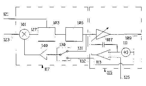
Figure 3 is a block schematic illustrating the aforesaid
prior transmitter from PCT Application WO-A1-95/23453. The
known transmitter is, in principle, divided into a phase
modulation control loop 117 and an amplitude modulation
control loop 115. The amplitude modulation control loop
includes a power amplifier 107, a directional coupler 109,
and an envelope detector 111 that is connected to one of the
signal inputs on the difference amplifier 113. An amplitude
reference signal 125 is applied to the other signal input.
The difference amplifier 113 generates a voltage difference
signal as a result of the difference between the two signal
inputs. The difference amplifier is connected to an input for
amplification control of the power amplifier 107. Amplitude
modulation of the output signal from the power amplifier is
achieved, by varying the voltage of an amplitude reference
signal.
The frequency translation of a phase reference signal 121 to
a correct channel frequency has been solved in this known
device with the phase modulation control loop 117. The loop
includes a mixer 101, a phase detector 103 and a voltage
controlled oscillator, VCO, 105 and a feedback coupling 131
from the oscillator output to a switch circuit 130. As before
mentioned, non-linear amplifiers exhibit pronounced phase
distortion at high powers. This distortion can be
CA 02259315 1998-12-22
WO 98/00909 ~ 10 PCT/SE97/01011
counteracted with a feedback 132 which is connected to the
output 109 of the power amplifier and which therewith
encloses the power amplifier in the phase modulation loop.
The inclusion of a switching circuit 130 in the phase
modulation control loop enables a switch to be made between
the two feedbacks 131 and 132. One of the feedback signals is
fed back to the mixer 301. The mixer generates an
intermediate frequency signal 127 whose frequency is equal to
the difference between a frequency reference signal 123 and
the signal that is fed back from the switching circuit 130.
The phase detector 103 generates an error signal that is
dependent on the phase difference of the intermediate
frequency signal 127 and the phase reference signal 121. The
error signal is applied to the frequency control input of the
oscillator. The oscillator output signal obtains in this way
a phase that is approximately equal to the phase of the phase
reference signal 121, meaning that the output signal has been
phase modulated with the phase reference signal 121. The
frequency of the output signal is dependent on the sum of the
alternative difference between the frequency of the frequency
reference signal and the frequencies of the phase reference
signal.
However,_ it is practically impossible to achieve fast locking
to the correct phase by switching between the two feedbacks
in accordance with the known method. The problem is that
upramping and downramping take place very quickly. Switching
between the two feedbacks results in a phase disturbance that
is unable to decay quickly enough. The loop loses its locking
in the worst of cases.
CA 02259315 1998-12-22
WO 98/00909 - 11 PCT/SE97/01011
It has been found more convenient to replace the switching
circuit 130 with a combining device, a combination circuit
that results in smooth transition between the two feedback
signal loops, in accordance with the present invention. When
the power amplifier is linear, the output signal from the
combination circuit to the phase detector is dominated by the
feedback signal from the output of the voltage controlled
oscillator at low power outputs. In the event of rapid
upramping of the output power with an increasing phase
distortion as a result, the signal contribution from the
feedback that includes the power amplifier will also
increase. This is dealt with by the combination circuit in
pace with the increase in the amplitude of the output signal.
The phase detector then has time to eliminate the phase
error. At full amplifier output power, the feedback output
signal fully dominates the combination circuit output signal.
The combination circuit may either be circuitry that includes
solely passive components, or circuitry that includes active
components (transistors).
An embodiment of a combination circuit that includes passive
components and a combination circuit that includes active
components will be described hereinafter. Both embodiments
include a limiting circuit. Limiting is necessary in order to
guarantee that the downstream mixer will operate correctly,
meaning that the mixer output amplitude will be constant. A
combination circuit constitutes an addition of the two
feedback signals sl and s2 in Figure 1A.
Figure 4 illustrates an embodiment of a combination circuit
CC1 that is implemented with passive components - in the
illustrated case resistances R1 and R2 - and a limiter LI.
CA 02259315 1998-12-22
WO 98/00909 ~ 12 PCT/SE97/01011
The feedback signals from sl and s2 in Figure lA are each
applied to a respective signal input 11 and 12. Each signal
input includes one of the respective resistances R1 and R2.
The signal inputs are connected to a common summation point
Asum for the signals sl and sz. A voltage source 13 is also
connected to the summation point Asum~ via a resistance R3.
The point Asum is connected to an input 14 on the limiter LI.
Since the signal sl is constant and also relatively weak in
comparison with the signal s2 that is fed back from the
output of the power amplifier, the signals will preferably be
weighted. Suitable choice of values of respective resistances
enables the two signals to be summated to a new signal ssum
which is limited in the limiter LI to a new feedback signal
s3 on the common output 15 of the limiter and the combination
circuit CC1. Weighting is effected so that the transition
from the state in which sl dominates in the feedback signal
s3 to the state in which S2 is dominant, and vice versa,
takes place at a suitable output power. It is determined that
the transition shall take place when the output power from s2
has become greater than PT (see Figure 1B) , where PT < Pmin-
By dominance is meant that one of the signals constitutes a
greater part of the feedback signal. As before mentioned,
limiting is necessary in order to guarantee that following
circuits.will operate correctly.
The described feedback of a signal s3 from the combination
circuit CC1 means that the power amplifier 3 (PA) in Figure
lA will be enclosed in a phase-locking loop to? the phase
modulation control loop 7 (PHC), which therewith phase-locks
the output signal s2 from the power amplifier 3.
CA 02259315 1998-12-22
WO 98/00909 ~ 13 PCT/SE97/01011
Figure 5 illustrates another advantageous embodiment of a
combination circuit CC2. This circuit CC2 is implemented with
active components. The circuit is an amplifier that has two
inputs 21 and 22. The signals that are fed back from sl and
s2 in Figure lA are each applied to a respective one of the
signal inputs 21 and 22. The amplifier includes two
transistors T1 and T2. The signal sl on the input 21 is
applied to the base of the transistor T1 via a biasing
circuit 23A. The signal s2 on the input 22 is applied to the
base of the transistor T2 via a biasing circuit 23B. Both
transistors are bipolar NPN transistors in the illustrated
case, although other types of transistors may be used. The
emitters of the transistors are connected to a common
constant current generator 24. The transistors are powered by
a drive voltage V~~ from a voltage source 25. The amplifier
has two arms. The collector of the transistor T1 is connected
to the voltage source 25 via the arm 26, and the collector of
the transistor T2 is connected to the voltage source 25 via
the other arm 27. As illustrated in Figure 5, each arm may
include a collector resistor R~. A signal sA flows from the
arm 26A, via a component 27A. A signal sB flows from the arm
26B, via a component 27B. The outputs of the resistances 27A
and 27B are connected to a common summation point A1S"m. This
point is. connected to an input 28 on the limit.er LI. The arms
26A and 26B are thus combined with the components 27A and 27B
in a manner to obtain a weighted sum sls"m of the feedback
signals sl and s2 at the point Alsum. The new signal Slsum is
limited in the limiter LI to a new feedback signal s3 on the
limiter output 29, which is also a signal output for the
combination circuit CC2.
CA 02259315 1998-12-22
WO 98/00909 - 14 PCT/SE97/01011
Feedback of the signal s3 from the combination circuit CC2
means that the power amplifier 3 in Figure lA will be
enclosed in a phase-locked loop to the phase modulation
control loop 7, which therewith phase-locks the output signal
s2 from the power amplifier 3.
Figure 6 illustrates a preferred embodiment of the inventive
phase distortion compensating device. The signal incoming to
the device is a phase signal ePhr, i.e. a signal in which the
information is found in the phase. The phase signal ePhr
contains the phase information to be modulated and
transmitted on an appropriate carrier frequency.
Frequency upconversion of the phase signal ephr to the correct
channel frequency is effected in a phase modulation control
loop for phase-locked and frequency upconversion. The loop
includes a mixer 30, a phase detector 31, a voltage
controlled oscillator, VCO, 32, an integrating filter circuit
34, a combination circuit 35 and a feedback 33 from the
output of the oscillator 32 to a first input of the
combination circuit 35 through the medium of a first tap
means 37. The oscillator 32 is connected to an input of a
power amplifier 40, the output of which is connected to an
antenna 50. The phase modulation control loop also includes a
second feedback 36 from the output of the power amplifier 40,
to a second input of the combination circuit 35 through the
medium of a second conductor means 38. This circuit may be
constructed in the manner described with reference to Figure
4 or to Figure 5.
The mixer 30 generates an intermediate frequency signal eifs
whose frequency is equal to the difference between a
CA 02259315 1998-12-22
WO 98/00909 - 15 PCT/SE97/01011
frequency reference signal efrs from a frequency synthesiser
39 and a feedback signal efab from the combination circuit 35.
The feedback signal efab corresponds to s3 in Figures 4 and 5.
The phase detector 31 generates an error signal ephf which is
dependent on the phase difference of the intermediate
frequency signal eifs and the phase signal ephr. The
integrating filter circuit 34 is connected between the phase
detector and the voltage controlled oscillator so as to
reduce the risk of phase distortion, noise transmission and
band broadening as a result of broadband noise. The filter
circuit effectively eliminates broadband noise. The noise
derives from sources within the phase detector. One such
source may be an IQ modulator used in certain types of radio
transmitter.
The error signal ephf is applied to the input of the filter
circuit 34 and from there to the frequency control input of
the oscillator 32. The output signal epha from the oscillator
32 thus obtains a phase that is approximately equal to the
phase of the phase signal ephr, meaning that the output signal
epha has been phase modulated with the phase signal ephr. The
frequency of the output signal epha is equal to the sum of or
the . difference between - the frequency of . the frequency
reference signal efr~ and the frequency of the phase signal
ephr
The signal ep::a is coupled to the power amplifier 40 which
amplifies the signal epha in response to the control signal
I~,mp. An antenna signal eout on the output of the amplifier 40
to the antenna 50 will then have the form determined by the
control signal Iam,p.
CA 02259315 1998-12-22
WO 98/00909 - 16 PCT/SE97/01011
If this embodiment is included in a transmitter that operates
in accordance with GSM standards, the output signal will
obtain the envelop presented in Figure 2B. The output signal
eout corresponds to the signal sz in Figure 1A, and the signal
epha corresponds to the signal sl.
The combining means, the combination circuit 35, receives a
part of the signal ePha and a part of the signal eQUt each
through the medium a respective signal tap 37 and 38. These
signal taps may have the form of directional couplers or some
form of voltage divider (capacitive or resistive taps). The
two loops 33 and 36 connect a respective tap 37 and 38 to its
particular input on the combination circuit 35. This combines
the two signals epha and eo"t from respective loops in
accordance with the amplification of the amplifier 40, to
provide a new feedback signal efab in the loop. The taps 37
and 38 each take out a specific part of respective signals
epha and eo"t . These taps may also be controllable . The
magnitude of respective signal parts that are taken out in
this way can therewith be controlled individually, which may
be to advantage. A controllable directional coupler is an
example of one such tap.
Before starting upramping of the power amplifier PA 40, the
loop is locked on the output signal from the voltage
controlled oscillator 32 with the aid of the first feedback
loop 33. As the output power increases in response to the
control signal IamP, the signal eout that is fed back from the
power amplifier output through the medium of the second
feedback loop 36 will gradually obtain domination over the
CA 02259315 1998-12-22
WO 98/00909 ' 17 PCT/SE97/01011
oscillator signal epha fed back through the medium of the
first feedback loop 33 as feedback signal efab.
Without the loop 33, phase-locking would not be achieved in
good time prior to activating the power amplifier, when
starting up the transmitter. When the loop has a sufficiently
broad bandwidth, the loop will have time to compensate for
the phase shift in the power amplifier 40 during upramping of
the output power. A feedback shall be established via the
loop 36 and said locking achieved in order to achieve the
intended phase distortion compensation at roughly 10 dB with
full output power.
The phase distortion compensating device of this embodiment
includes an amplifier 40 that has an input connected to an
output of a phase-locking and upconversion loop. This loop
includes a first and a second feedback loop, 33 and 36
respectively, wherein the first feedback loop 33 is connected
to tap means 37 for tapping off a part of a modulated signal
on the power amplifier input, and the second feedback loop 36
is connected to a tap means 38 for tapping off a part of the
amplified modulated signal on the output of the power
amplifier 40.
Each of the loops 33 and 36 is connected to a respective
input of the combining means 35, which combines the two input
signals from respective loops so as to generate a new
feedback signal in the loop.
The phase distortion compensating method according to this
embodiment involves combining the two signals ePha and eo"t
from respective loops 33 and 36 to generate the new feedback
CA 02259315 1998-12-22
WO 98/00909 - 18 PCT/SE97/01011
signal efab in the loop. If amplification in the amplifier 40
changes, the proportionality in which the feedback signals
are fed back and their dominance in the feedback signal to
the phase-locking and upconversion loop will also change. The
inventive method provides a smooth and continuous transition
between the parts of the signals that are fed back and
therewith the dominance in the feedback signal, so as to
enable the phase-locking and upconversion loop to be phase-
locked in time before a rapid change in the output power of
the power amplifier begins to take place, while maintaining
phase-locking during upramping and downramping. In accordance
with the inventive method, the dominance in the new feedback
signal of the feedback signal that is taken out from the
output of the power amplifier 40 increases with increasing
amplifier output powers. The signal fed back from the power
amplifier output is dominating in the new feedback signal
when the power amplifier amplifies with full output power,
whereas the signal fed back from the power amplifier input is
dominating in the new feedback signal when the amplifier
output power is low.
As a result of the inventive method, the phase-locking and
upconversion loop is locked onto the modulated signal epha on
the .input of the power amplifier 40 before tie output power
of the power amplifier increases. When upramping of the
amplifier has begun, the phase-locking and upconversion loop
is locked onto the amplified modulated signal on the power
amplifier input before the output power of the power
amplifier has reached its full strength.
Figure 7 illustrates an embodiment which differs slightly
from the inventive device illustrated in Figure 6. According
CA 02259315 1998-12-22
WO 98/00909 ~ 19 PCT/SE97/01011
to the block schematic shown in Figure 6, the phase
modulation control loop includes the phase detector 31, the
filter circuit 34, the oscillator 32, the combination circuit
35, the mixer 30 and the local oscillator 39. The phase
modulation control loop in Figure 7 also includes a sweep
circuit 60 (SVP) connected between the voltage controlled
oscillator 32 (VCO) and the filter circuit 34. In order to
ensure fast phase-locking of the loop, the control voltage of
the oscillator VCO is swept over the voltage interval in
to which the oscillator is expected to lock. The sweep can be
initiated and stopped with a control signal Ist on a control
input 61 of the sweep circuit 60. The frequency of the
oscillator output signal is varied, by varying the control
voltage to the oscillator.
Figure 8A illustrates the principle of time-controlling the
phase-locking of the device shown in Figure 7 with the aid of
a time axis and marked time points . A start pulse Ist starts
the sweep circuit at time point ts~ and the output voltage of
the circuit to the voltage controlled oscillator 32 is
changed with time in accordance with a predetermined function
over a suitable voltage interval in which the loop is
expected to lock. Sweeping of the voltage interval is
commenced in good time before the time point t"P at which
upramping of the output power from the power amplifier 40
(PA) commences. It is necessary that the sweep circuit 60 has
time enough to sweep once over the voltage interval. The loop
locks at an arbitrary time point tl~x and remains locked
during uprampir_g and downramping, which occur at respective
time points t"p and tdoWn. The loop can be kept locked because
the combination. circuit 35 produces a "smooth" successive
transition fro;-. one feedback loop 33 to the other feedbaclc
CA 02259315 1998-12-22
WO 98/00909 ~ 2 0 PCT/SE97/01011
loop 36. On the other hand, phase-locking is lost when a fast
switch is made, therewith resulting in a loss of information
in the output signal from the power amplifier.
The sweep circuit 60 is supplied with a voltage signal es~,
from the filter circuit 34. A voltage signal e~~o is delivered
from the output of the sweep circuit to the voltage
controlled oscillator 32. The signals es~, and e"~o include the
phase information to be transmitted. The sweep circuit 60
adds the sweep to the information in es~. A start pulse ISt
is applied to the sweep circuit input 61 at time point ts~.
The sweep circuit 60 then begins to vary e~~o with time, in
accordance with a predetermined time function. Figure 8B
illustrates an example of how the signal e"~o can be swept by
the sweep circuit 60 and varies with time t over a desired
voltage interval Vint=[Vstart, Vstop~ . The voltage is lowered
linearly from a constant high value vstart when commencing the
voltage sweep. The frequency of the output signal from the
oscillator 32 is changed when e~~o is changed. In Figure 8B,
the loop locks, Vlo~k, when eV~o controls the voltage
controlled oscillator 32 so that eifs=ephr. This occurs at the
arbitrary time point tl~x. The signal e~~o is maintained at
Vlo~k until the output power is tamped down at time point te"a.
The voltage sweep is restarted from the voltage ~l5tart upon
the arrival of the next start pulse.
The start pulse Ist is generated when starting up the
transmitter and may be generated in a control part of the
radio transmitter. The sweep circuit can be programmed, to
enable different sweep contro7_ parameters to be stored in a
CA 02259315 1998-12-22
WO 98/00909 ~ 21 PCT/SE97/01011
sweep circuit control unit. The voltage interval
VintUVstart ~ U9toP~ to be scanned can therewith be determined as
a time interval from the time that a start pulse ISt is
sensed on the control input 61 of the sweep circuit 60.
Figure 9 is a flowchart illustrating a method of compensating
for phase distortion in accordance with the inventive
concept. Certain of the reference signs used in the following
text are to be found in Figures 6 and 7. The method relates
to phase distortion compensation in a power amplified
modulated signal on the output of the power amplifier 40,
wherein the amplifier has an input connected to an output on
a phase-locking and upconversion loop (30-39) {the loop is
also designated phase modulation control loop). The loop
includes the first and the second feedback loop 33 and 36
respectively. The method commences at the upstart of the loop
in a start position 200. In a first step 202 of the method,
part of the modulated signal epha on the input of the power
amplifier 40 is taken out, or tapped off, via the first
feedback loop 33. In step 204, a part of the amplified
modulated signal eout on the output of the power amplifier 40
is taken out, or tapped off, via the second feedback loop 36.
In a third step 206, the two signals that were tapped off are
combined in the combining means 35 to provide a feedback
signal efab that contains both of the tapped-off signals. In a
following step 208, the feedback signal is fed back to the
phase-locking and upconversion loop. The loop phase-locks the
output signal eout onto the phase reference signal ePhr in the
next step 210, and therewith compensates for phase distortion
in the output signal eout of the power amplifier. When the
amplifier output power changes, the combining means 35
CA 02259315 1998-12-22
WO 98/00909 - 2 2 PCT/SE97/01011
combines the two signals that were tapped off such as to
change their relative dominance in the feedback signal in a
smooth transition, so as not to lose the phase-lock and
therewith the phase distortion compensation, this being
effected in step 212. The method is continued whilst the loop
is in operation and is not interrupted until the transmitter
in which the loop is included is no longer switched on.
This step 214 is illustrated in the flowchart by a return to
step 212. A termination position, step 216, is adopted
immediately the transmitter is switched off.
Because the inventive method provides a smooth and continuous
transition between the mutual proportionality of the tapped-
off signals in the feedback signal, and therewith the
relative dominance of said signals in the feedback signal,
the phase-locking and upconversion loop can be phase-locked
in good time before a rapid change in the output power of the
power amplifier begins. It had not been possible to achieve
such phase-locking with prior art techniques in which a
switch is used to switch between the two feedback loops. Such
a technique introduces a high degree of sensitivity when
switching takes place. There is also the risk of introducing
a transient in the loop. when switching takes place. Such
transients can cause the phase-lock to be lost together with
valuable information in the loop input signal.
No transients will be introduced into the closed loop when
practising the inventive method.
The inventive method and the inventive device solve the
aforementioned problems associated with phase compensation in
different applications, such as in radio telecommunications,
etc.