Note: Descriptions are shown in the official language in which they were submitted.
CA 02259644 1999-02-OS
1
Synchronization set for a synchronous digital message
transmission system and process for producing
a synchronous output signal
The invention relates to a piece of a synchronization set
for a synchronous digital message transmission system for
producing a synchronous output signal out of a digital
input signal in accordance with the topic of claim 1 and a
process for producing a synchronous output signal in
accordance with the topic of claim 8.
A piece of a synchronization set for SDH or SONET systems
is known from the conference article "SONET/SDH Pointer
Processor Implementation" by M. Klein and R. Urbansky, 1994
IEEE GLOBECOM Communications: The Global Bridge, San
Francisco, November 28-December 2, 1994, pp. 655-660, such
systems producing a synchronous output signal from
plesiochronic or pseudosynchronic digital input signals. In
addition, the input signals are written bit by bit with a
write clock into buffer memory and read again with a read
clock in order to form the synchronous output signal. Under
this application, the read clock has to be synchronized to
a reference clock pulse of the message transmission system,
specifically with the precision set forth in ITU-T G.813
for SDH systems of ~4.6 ppm.
The output signals produced thus are transported over the
message transmission system and reintegrated at the other
end, using a desynchronization set, into their original
plesiosynchronous or pseudosynchronous message signals. A
CA 02259644 1999-02-OS
2
difficulty that can emerge because of transmission is that
low-frequency phase fluctuations can be added up that are
caused by the intermediary saving in different buffer
memories of the message transmission system. Such low-
frequency phase fluctuations are characterized as wanders
and can lead to exceeding buffer memory and any data loss
tied to this. The conference article suggests avoiding such
wanders by modulating the decision level of the pointer
processor with a constant frequency. This wave modulation
is however technologically expensive since all network
elements have to be changed to deviate from the
standardization. In addition, the wave modulation leads to
a considerable increase of fitter in the message
transmission system.
The task of the invention is to give a synchronization set
for a synchronous digital message transmission system as
well as a process for producing a synchronous output signal
through which the low-frequency phase fluctuations are
minimized in another, technologically less expensive
fashion.
The task is solved with respect to the synchronization set
through the characteristics of claim 1 and with respect to
the process through the characteristics of claim 8.
Advantageous reconfigurations can be interpolated from the
dependent claims.
Beside the lessening and avoidance of wanders, another
advantage of the invention is that both the synchronization
set as well as the desynchronization set on the other end
of the transmission leg and intermediarily switched network
CA 02259644 1999-02-OS
3
elements of the synchronous digital message transmission
system come out with smaller buffer memories than until
now. Another advantage of the invention is that the
duration of message signals through the message
transmission system is diminished whenever the write clock
is less than the read clock because the filling level of
all buffer memory of the transmission leg then lies at the
bottom limit. Another advantage of the invention is that
the synchronization set in accordance with the invention is
compatible with existing message transmission systems.
With another especially advantageous construction of the
invention as under subclaim 7, an input signal is divided
and packaged in a parallel fashion into several
subassemblies of synchronous transport modules. These
several subassemblies are saved intermediarily with the
write clock in the buffer memory and with the higher or
lower read clock in such a way that several synchronous
output signals are created. The particular advantage of
this additional construction is that now input signals, for
example ATM signals (asynchronous transport mode) or
digitized video signals, can be processed that would
explode the transportation capacity of a single virtual
container. Through intermediary saving with the write clock
in accordance with the invention - the write clock being
lower than the read clock - phase fluctuations, i.e.
differences in transmission time, of the different virtual
containers can be avoided. Thus, a desynchronization set at
the other end of the synchronous message transmission
system achieves the simple integration of the transported
portions packaged in several subassemblies that are from
CA 02259644 1999-02-OS
4
the original input signal put back into their original
form.
Below, three examples of how the invention can be
implemented using Figures 1 through 6d are explained. They
show:
Figure 1 a synchronous digital message transmission system
with synchronization and desynchronization set,
Figure 2 a block diagram of the synchronization set in
accordance with the invention in the first example
of implementation,
Figure 3 a block diagram of the synchronization set in
accordance with the invention in the second
example of implementation,
Figure 4 a block diagram of the synchronization set in
accordance with the invention in the third example
of implementation,
Figure 5 a flowchart of the process in accordance with the
invention, and
Figures 6a through 6d: applications of the invention.
In Figure 1, the synchronous digital message transmission
system SDH of the example of implementation is shown
schematically. It regards a number of network elements
linked together among themselves such as cross-connect
device and add/drop multiplexers. A synchronization set
SYNC constitutes the interface between the synchronous
digital message transmission system and a plesiochronic
message transmission system. The synchronization device
receives as an input signal a plesiochronic message signal
PDH and produces out of it a synchronous message signal
CA 02259644 1999-02-OS
STM-N that sends them into the synchronous digital message
transmission system SDH. Over a pathway PATH of the message
transmission system that runs over a number of
intermediarily switched network elements NE shown as an
example, the synchronous message signal STM-N is
transmitted to the desynchronization set. There, it is
again reintegrated to the original plesiochronic message
signal PDH.
A synchronous message signal STM-N consists of successive
synchronous transport modules that are synchronized to a
frame clock. The synchronous message signal STM-N is
synchronized to a reference clock pulse uniform in the
entire synchronous message transmission system. So that a
plesiochronic message signal can be transmitted over a
synchronous digital message transmission system, it has to
be packaged into the usage burden of the synchronous
transport modules. The synchronization set performs this.
A basic idea of the invention is in packaging input signals
first in subassemblies of the synchronous transport
modules, so-called virtual containers VC-N in the sie N
(N=11, 12, 2, 3, or 4), lowering or raising the effective
bit rate of the virtual contains in comparison with the
standardized value (see ITU-T G.707, 03/96, Chapter 6.1),
or multiplexing. Thus, the filling level of buffer memories
of intermediarily switched network elements can be stored
in the area of the lower and/or upper limit and kept
constant, thus diminishing an adding of wanders.
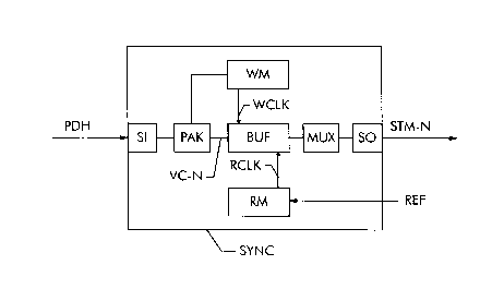
In Figure 2, the block diagram of a synchronization set
SYNC in accordance with the invention is shown in a first
CA 02259644 1999-02-OS
6
example of implementation. It contains a receiver unit SI,
e.g. a interface switching with optoelectric wanders (e. g.
following ITU-T G.703) that receives a digital input signal
PDH. For the input signal, it is a question of a
plesiochronic message signal. From the receiver unit, the
received message signal is conducted further to the package
assembly device PAK that packages it in subassemblies of
the synchronous transport modules, so-called virtual
containers VC-N. The data bits of the input signal packaged
this way are then written using a writer WM with a write
clock WCLK into the buffer memory BUF. The writer WM
includes a clock pulse generator for the write clock WCLK.
Using a reader RM, the data bits are then read back out
with a read clock RCLK and routed to a multiplex device
MUX, which multiplexes the subassemblies that now are
synchronized to the read clock into the transport modules.
Multiplexing occurs as described in ITU-T G.707, 03/96,
Chapter 6.1.
In accordance with the invention, the write clock WCLK is
lower than the read clock RCLK. The read clock RCLK is
synchronized to the reference clock pulse of the message
transmission system. Through this, the effective bit rate
of the virtual container in comparison to the value set
forth in the standard is lowered. The difference between
the effective bit rate of the virtual container VC-N and
the standardized bit rate is balanced out through stuffing
procedures that are characterized as pointer actions
(pointer justification).
The write clock WCLK can be chosen advantageously by 4.6
ppm lower than the read clock RCLK. A deviation of the bit
CA 022S9644 1999-02-OS
7
clock pulse of sent output signals from the reference clock
pulse of the message transmission system of 4.6 ppm is the
maximum permitted deviation under ITU-T G.813. Particularly
advantageous is the write clock, however, chosen by more
than 4.6 ppm lower than the reference clock pulse in order
to effect that the buffer memory of a11 intermediarily
switched network elements in the transmission pathway
through the message transmission system always remain on
the lower filling limit at any permissible synchronization
state. Thereby, the emergence of wanders is inhibited. Of
course, through the stuffing process jittering can arise,
but this can however be removed in the desynchronization
set on the other end of the transmission pathway to a
sufficient degree through deep pass filtering.
The write clock is even less selected than the read clock
such that the maximum permitted rate in the synchronous
digital message transmission system is achieved at stuffing
processes. As long as this maximum permitted rate is not
exceeded, the output signal can b transported over existing
SDH networks or SONET networks. However, the less the write
clock, the higher the frequency of fitter arising from
balancing pointer actions and the better this fitter can be
removed through deep-pass filtering. For this reason, the
write clock can be selected up to 200 ppm lower than the
read clock and/or the reference clock pulse of the message
transmission system.
Beyond plesiochronic message signals, other digital input
signals can also be transmitted over the digital
synchronous message transmission system, such as coded
video signals, for example.
CA 02259644 1999-02-OS
8
A second example of implementation of the invention is
shown in Figure 3 in a block diagram. The synchronization
set SYNC2 has, as in the first example of implementation, a
means of input SI, a means of output SO, buffer memory BUF,
a package assembly device PAK and a multiplexing device
MUX. Unlike the first example of implementation, the
synchronization device possesses a clock pulse generation
CG that is synchronized to the reference clock pulse REF of
the message transmission system. This clock pulse generator
takes care of a11 machine-internal construction groups,
such as the multiplexing device with a clock pulse signal.
This clock pulse signal also serves as read clock RCLK.
Between clock pulse generator CG and the write clock input
of the buffer memory BUF, a clock pulse adaptation switch
ADA is turned on that lowers the clock pulse of the clock
pulse generator CG in order to generate the write clock
WCLK. Thereby it is achieved that the write clock is lower
than the read clock.
In an advantageous further construction of the invention,
this clock pulse adaptation switch is adjustable and
controllable such that the write and read cycle agree at
least in the limits standardized for the clock pulse
deviation in SDH. Through this it can be achieved that the
function can be turned off in order to use a lower write
clock so that the synchronization set in accordance with
the invention can work together with the usual
desynchronization sets. Turning on and off is controlled
advantageously through a message in the frame head
(overhead) of sent transport modules. Using this message,
the desynchronization set is shared on the other end of the
transmission pathway that the bit rate of the virtual
CA 02259644 1999-02-OS
9
container VC-N is lowered to the invention-related way. In
addition, a bit or byte reserved for company-specific
applications is used advantageously in the frame-tip of
synchronous transport modules. In an advantageous fashion,
the desynchronization device leaves a receipt for the
message and thus allocates to the synchronization set its
ability to process the expected high rate of pointer
actions. The desynchronization set can additionally have
narrow-band clock pulse filtering with a bandwidth in the
area of 10 to l00 mHz.
In accordance with the third example of implementation
shown in Figure 4 of a synchronization set SYNC3, two
virtual containers VC-N are formed from the packet assembly
device PAK out of the input signal ATM. This also means
that two virtual containers are used independently from
each other which indicate the different virtual connections
through the synchronous digital message transmission
system. The several virtual containers VC-N have a lower
bit rate in accordance with the invention than prescribed
by G. ITU-T G.707, 03/96, Chapter 6.1, and are written with
the write clock WCLK lowered by the clock pulse adaptation
switch ADA into the buffer memory BUF. They are then read
back out of the buffer memory BUF with the read clock RCLK
that is produced by the clock pulse generator CG of the
synchronization set SYNC3 and is synchronized to the
reference clock pulse REF of the message transmission
system. The reading occurs in such a way that of two
multiplexer devices MUX1 and MUX2 there are several
synchronous output signals built STM-N1, STM-N2. The two
synchronous output signals STM-N1, STM-N2 are then
transmitted by two sending units SO over the synchronous
CA 022S9644 1999-02-OS
message transmission system. On the other end of the
message transmission system, the usage burden of both
output signals STM-Nl and STM-N2 can then be unpackaged
again and reintegrated into the original input signal ATM.
The measures depicted in the third example of
implementation for dividing an input signal and for
transmitting it packaged in several virtual containers, is
characterized as virtual concatenation described in ITU-T
G.707, 3/96, Chapters 8.1.7.2 and 8.3.6.2. This measure can
10 be applied, for example, when the bit rate of the input
signal is higher than the maximum usage burden of the
virtual containers. Thus, input signals can also be
transmitted with a transmission rate of more than l40
Mbit/s (the capacity of a VC-4 is 139,264 kbit/s) in the
synchronous digital message transmission system. Through
the use in accordance with the invention of virtual
containers with a bit rate reduced in comparison to the
standard, it is advantageously achieved that the phase
deviation arising because of wanders between the several
virtual containers are minimal, which makes the integration
in the desynchronization possible on the other end of a
transmission pathway.
In Figure 5, a flow chart is shown with the process in
accordance with the invention of producing a synchronous
output signal. Successive steps must be executed:
Step Sl: A digital input signal is received at a
synchronization set over a receiver unit that is a
PDH interface in the examples of implementation.
CA 02259644 1999-02-05
11
Step S2; The digital input signal is packaged using a
package assembly device in subassemblies of
synchronous transport modules, so-called virtual
containers.
Step S3: The data bits of the virtual container are written
after each other with the write clock of a writer
into buffer memory.
Step S4: The data bits are read back out with the read
clock of a reader from the buffer memory in order
- to form the synchronous output signal. Here, the
read clock is higher than the write clock,
preferentially by at least 4.6 ppm.
Step S5: The output signal is sent over a sending unit into
the synchronous digital message transmission
system.
Between steps S4 and S5, a multiplexing of several virtual
containers can take place into the synchronous transport
modules. Then, several input signals are packaged with a
bit rate lower than the standardized one into virtual
containers.
Applications of the invention are shown in Figures 6a
through 6d. In Figure 6a, it can be seen that the digital
input signal PDH, a plesiochronic message signal, is
produced by a exchange point VS, over a invention-specific
synchronization set SYNC, a synchronous digital message
transmission system SDH and a desynchronization set DESYNC
is sent to a concentrator RSU. Here, the exchange point VS
synchronizes the concentrator RSU with the help of the
plesiochronic message signal PDH transmitted this way.
This is possible because, thanks to the invention, low-
CA 02259644 1999-02-OS
12
frequency phase fluctuations do not occur in the message
signal. In Figure 6b it is shown that the invention-
specific synchronization set SYNC can also be integrated
into the exchange point.
In Figure 6c, a coding device COD for video signals
produces the digital input signal DVB, a digital video
signal. It can for example be a question of VoD or DVB
signals (VoD: video on demand; DVB: digital video
broadcasting) or also a question of signals with a bit rate
of 34 or 140 Mbit/s. The input signal DVB is sent as in
Figure 6a over synchronization set, synchronous digital
message transmission system and desynchronization set to a
decoding device DEC for digital video signals. This is
advantageous because, with this construction, thanks to the
invention, also possible is synchronizing the decoding
device DEC with the transmitted digital video signal DVB to
the coding device COD. In Figure 6d it is shown that the
invention-specific synchronization set SYNC can also be
integrated into the coding device COD and that the
dysynchronization set DEC can also be integrated into the
decoding device DEC.
The write clock is always selected lower in the examples of
implementation than the read clock. This form of
implementation is preferred because this way it can be
achieved that the signal durations are minimal through the
synchronous digital news transmission system since a11
buffer memory of network elements are in the transmission
pathway on the lower filling level. The invention is
however also deployable with a positive frequency offset,
i.e. with a write clock higher in comparison to the read
CA 02259644 1999-02-OS
13
clock because wanders is avoided in an execution because
the filling level of the buffer memory is then at the upper
limit.