Note: Descriptions are shown in the official language in which they were submitted.
CA 02259838 1999-02-10
74078-32
SUBSTITUTE SPECIFICATION
METHOD AND APPARATUS FOR RETRIEVING
DATA FROM A STORAGE DEVICE
This invention relates to storage and retrieval of data
stored on various magnetic and/or electronic media and, more
particularly, to a method and apparatus for storing and retriev-
ing data in a magneto-optical disk system.
Various types of recordable and/or erasable media have
been used for many years for data storage purposes. Such media
may include, for example, magnetic tapes or disks in systems
having a variety of configurations.
Magneto-optical ("MO") systems exist for recording data
on and retrieving data from a magnetic disk. The process of
recording in a magneto-optical system typically involves use of a
magnetic field to orient the polarity of a generalized area on
the disk while a laser pulse heats a localized area, thereby
fixing the polarity of the localized area. The localized area
with fixed polarity is commonly called a pit. Some encoding
systems use the existence or absence of a pit on the disk to
define the recorded data as a "1" or "0", respectively.
When recording data, a binary input data sequence may
be converted by digital modulation to a different binary sequence
having more desirable properties. A modulator may, for example,
convert m data bits to a code word with n modulation code bits
(or "binits"). In most cases, there are more code bits than data
bits -- i.e., m < n.
1
CA 02259838 1999-02-10
Most if not all disk drive systems use run-length-
limited ("RLL") modulation codes, such as RLL 2/7/1/2 or RLL
1/7/2/3 codes. Another family of modulation codes are group-
coded recording ("GCR") codes, such as GCR 0/11/8/9 or GCR
0/3/8/9 codes (sometimes abbreviated as GCR 8/9). The numbers
appended to the names of particular codes typically refer to
certain encoding constraints, such the relationship between bits
and flux reversals, or the minimum and maximum number of contigu-
ous binits possible without flux transitions. For example, a
commonly used encoding system for pit-type recording is the RLL
2/7/1/2 code which constrains the recorded information to have a
minimum of two and a maximum of seven zeroes between ones. In
general, RLL recording provides a relatively high data-to-pit
ratio but may not, however, in many circumstances allow for high
data storage densities because amplitude and timing margins
deteriorate very rapidly as frequency is increased.
A GCR 0/3/8/9 code, on the other hand, not only re-
quires nine flux reversals for every eight data bits but further
requires a minimum of no zeroes and a maximum of three zeroes
between ones.
The density ratio of a given recording system is often
expressed according to the equation (m/n) x (d + 1), where m and
n have the definitions provided above, and d is defined as the
minimum number of zeroes occurring between ones. Thus, the RLL
2/7/1/2 code has, according to the above equation, a density
ratio of 1.5, while the GCR 0/3/8/9 code has a density ratio of
0.89.
For reading data in an MO system, a focused laser beam
or other optical device is typically directed at the recording
surface of a rotating optical disk such that the laser beam can
2
CA 02259838 1999-02-10
selectively access one of a plurality of tracks on the recorded
surface. The rotation of the laser beam reflected from the
recorded surface may be detected by means of Kerr rotation. A
change in Kerr rotation of a first type, for example, represents
a first binary value. A change in Kerr rotation of a second type
represents a second binary value. An output signal is generating
from the first and second binary values occurring at specified
clock intervals.
Although there has been a continual demand for disk
systems capable of storing increasingly higher data densities,
the ability to achieve high data storage densities has met with
several limitations. As a general matter, the reasonable upper
limit for data density is determined in part by reliability
requirements, the optical wavelength of laser diode, the quality
of the optical module, hardware cost, and operating speed.
Maximum data densities are also affected by the ability to reject
various forms of noise, interference, and distortion. For
example, the denser that data is packed, the more intersymbol
interference will prevent accurate recovery of data. Moreover,
because the technology for.many intermediate and high performance
optical disk drives has been limited by downward compatibility
constraints to older models, signal processing techniques have
not advanced as rapidly as they might otherwise have.
When attempting to recover stored data, existing read
channels of magneto-optical and other types of disk drives
commonly suffer from a number of problems due to the unintended
buildup of DC components in the read signal. One cause of DC
buildup results from the recording of unsymmetrical data patterns
over a number of bytes or data segments. A symmetrical data
pattern may be considered as one having an average DC component
3
CA 02259838 1999-02-10
of zero over a region of interest. Because sequences of recorded
bits may be essentially random in many modulation codes, however,
localized regions of recorded data having particular patterns of
1's and 0's will produce an unsymmetrical read signal having
unwanted DC components. Because the data patterns vary over
time, the level of DC buildup will also vary, causing wander of
the DC baseline, reduction of threshold detection margins, and
greater susceptibility to noise and other interference.
Undesired DC buildup is also caused by variance in pit
size due to thermal effects on the writing laser or the storage
medium. As the writing laser heats up, for example, the spot
size may increase leading to wider pits. When the recorded pits
are read, variations in pit size will cause an unsymmetrical
input signal having DC components. Variation in pit size not
only causes undesired DC buildup but also causes the relative
locations of the data to appear shifted in time, reducing the
timing margin and leading to possible reading errors.
Various attempts have been made to overcome the de-
scribed problems. For example, various tape drive systems
commonly use a DC-free code such as a 0/3/8/10 code, otherwise
referred to simply as an 8/10 code. Because an 8/10 code re-
quires 10 stored bits to yield 8 data bits, however, it is only
80% efficient which is a drawback when attempting to record high
data densities.
Another method for handling DC buildup involves the use
of double differentiation. This method typically involves
detection of the peaks of a first derivative of the input signal
by detecting zero-crossings of the second derivative of the input
signal. Thus, the DC components are effectively filtered out.
One drawback of this method is that differentiation or double
4
CA 02259838 1999-02-10
differentiation can cause undesirable noise effects. A second
drawback is that the method may decrease the timing margin to
unacceptably low levels (e.g., by as much as 50 percent?.
In another method for addressing DC buildup, the data
to be stored is randomized prior to recording such that none of
the data patterns repeat over a data sector. However, this
method may not acceptable by ISO standards and may lack downward
compatibility with previous disk drive systems. As a further
drawback to this method, de-randomizing the data may be complex.
Yet another method for controlling DC buildup involves
the use of so-called resync bytes between data segments. This
method generally involves the examination and manipulation of
data before it is recorded in order to minimize DC buildup upon
readback. Before recording, two consecutive data segments are
examined to determine if the patterns of 1's and 0's are such as
to cause positive DC, negative DC, or no DC components when read
back. If, for example, two consecutive data segments have the
same DC polarity, one of the data segments is inverted prior to
being recorded on the medium. In order to stay within the
constraints of the particular encoding system, however, a resync
byte between the segments may need to be written so that the
pattern of contiguous bits and of flux reversals is proper. A
drawback of such a method is that it will not necessarily reduce
all DC buildup, and time constants must be determined such that
the predictable DC buildup will not affect performance. Further,
the method requires additional overhead including the examination
of data segments to determine their relative polarity.
It would therefore be advantageous to have a method and
device for reading stored data from a medium without suffering
the undesirable effects of DC buildup, without creating unaccept-
5
CA 02259838 1999-02-10
able levels of noise or significantly reducing timing margins,
without the requirement of large amounts of overhead or
derandomizing algorithms, and while providing high data
storage efficiency.
An apparatus and method is provided for retrieving
densely stored data from various types of magnetic media. One
embodiment of the invention generally comprises the steps of
differentiation, equalization, partial integration, and data
generation. The steps of differentiation, equalization and
l0 partial integration may generally provide a preprocessed
signal corresponding to a playback signal but with better
resolution and reduced noise. Data generation may further
comprise the steps of detecting the positive and negative
peaks of the preprocessed signal in a manner so as to account
for the DC component, and generating a threshold corresponding
to the midpoint of the measured positive and negative peak
values. The method further may involve the step of feeding
back a signal indicative of variations in the duty cycle of
the output signal so as to enable tracking of the DC component
20 by positive and negative peak detection circuits.
In accordance with the present invention, there is
provided an apparatus for locating transitions in a signal
having a DC component, said apparatus comprising: means for
reading data stored on a medium and generating a signal
representing the stored data; waveform restoration means for
restoration of said signal, said waveform restoration means
receiving said signal and producing a restored signal; a
threshold generator means for generating a threshold level
6
74078-32D
CA 02259838 1999-02-10
from said restored signal; a data generator means for
generating a data output from said restored signal and said
threshold level, said data generator including a comparator
means for processing of said restored signal and said
threshold level; and a feedback means for providing a feedback
path from said comparator means to said threshold generator
means.
In accordance with another aspect of the invention,
there is provided a partial integrator stage for use in
processing a playback signal in the read channel of an
information storage system, said partial integrator stage
comprising: a first differential amplifier receiving the
playback signal, said differential amplifier generating an
amplifier output; a current generator receiving and processing
said amplifier output, said current generator producing a
first output and a second output; a bandpass filter receiving
and processing said first output from said current generator
to thereby generate a bandpass filter output; an integrator
stage receiving and processing said second output from said
current generator to thereby generate an integrator stage
output; and a subtractor stage receiving said bandpass filter
output and said integrator output, said subtractor stage
subtracting said bandpass filter output from said integrator
stage output to thereby generate a partial integration output.
In accordance with another aspect of the invention,
there is provided an apparatus for locating transitions in a
signal having a DC component, said apparatus comprising: a
data detection device reading stored data and generating a
6a
74078-32D
CA 02259838 1999-11-22
signal representing said stored data; a waveform restorer
processing said signal and producing a restored signal output;
a threshold generator generating a threshold level from said
restored signal; a data generator generating a data output
from said restored signal and said threshold level, said data
generator including a comparator for processing of said
restored signal and said threshold level; and a feedback path
from said comparator to said threshold generator.
In accordance with another aspect of the invention,
there is provided a method for retrieving data stored on a
medium, said method comprising the steps of: reading said
stored data to thereby generate a playback signal; partially
integrating said playback signal; generating a threshold
signal which varies with a DC component of said partially
integrated signal; and generating an output signal indicative
of said stored data by comparing said partially integrated
signal with said threshold signal wherein the step of
partially integrating comprises: integrating said playback
signal; simultaneously with but separately from said
integrating, bandpass filtering said playback signal; and
taking a difference between said integrated signal and said
bandpass filtered signal to thereby generate a difference
signal.
In accordance with another aspect of the invention,
there is provided an apparatus for retrieving data stored on a
medium, said apparatus comprising: means for reading said
stored data and generating a signal corresponding to said
stored data; a differentiation stage for processing said
signal prior to partial integration thereof; a partial
6b
CA 02259838 1999-11-22
integrator for receiving said signal; a threshold generator
connected to said partial integrator; a data generator
connected to said partial integrator and to said threshold
generator, said data generator including a comparator; and a
feedback path from said comparator to said threshold
generator.
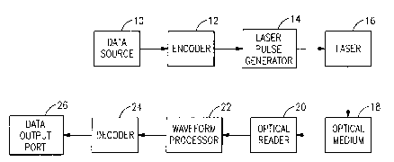
FIG. 1 is a block diagram showing an optical data
storage and retrieval system;
FIG. 2 is a series of sample waveforms associated
with a GCR format;
FIGS. 3A and 3B are waveform diagrams of a
symmetrical and unsymmetrical input signal, respectively;
FIG. 4 is a block diagram of a read channel;
FIG. 5 is a more detailed block diagram of various
stages of a read channel;
6c
CA 02259838 1999-02-10
FIG. 5B is a detailed circuit diagram of a partial
integrator stage;
FIGS. 6A-6E are frequency response diagrams of various
stages of a read channel;
FIG. 6F is a plot of group delay for a combination of
stages in a read channel;
FIG. 6G is a waveform diagram showing signal waveforms
at various stages in the read channel;
FIG. 7 is a block diagram of a peak detection and
tracking circuit;
FIG. 8 is a schematic diagram of the peak detection and
tracking circuit of FIG. 7;
FIG. 9 is a waveform diagram showing tracking by a
threshold signal of the DC envelope of an input signal;
FIGS. l0A-lOD are diagrams showing exemplary waveforms
at various points in a read channel;
Fig. 11 is a series of waveforms showing uniform laser
pulsing under a pulsed GCR format and non-uniform laser pulsing
under an RLL 2,7 format;
Fig. 12 is a series of waveforms showing laser pulsing
for various data patterns adjusted by the write compensation
circuit;
Fig. 13 is a schematic diagram showing the write
compensation circuit;
Fig. 14 is a series of waveforms showing laser pulsing
for amplitude asymmetry correction;
Fig. 15 is a schematic diagram showing the amplitude
asymmetry correction circuit;
Fig. 16 is a block diagram showing the basic relation-
ship of elements of the pulse slimming means;
7
CA 02259838 1999-02-10
Fig. 17 is a series of waveforms showing threshold
adjustments by the dynamic threshold circuit;
FIG. 18 is a schematic diagram for the dynamic
threshold circuit; and
FIG. 19 is a schematic block diagram of an optical
data storage and retrieval system incorporating downward
compat ibi 1 it y .
Although the present invention is applicable to many
different data storage and retrieval systems, the following
description of the preferred embodiment will focus primarily
on magneto-optical systems. In so doing, there is no intent
to limit the scope of the invention solely to devices which
are magneto-optical in nature.
A block diagram of an exemplary magneto-optical
system is shown in Fig. 1. The system may have a read mode
and a write mode. During the write mode, a data source 10
transmits data to an encoder 12. The encoder 12 converts the
data into binary code bits. The binary code bits are
transmitted to a laser pulse generator 14, where the code bits
may be converted to energizing pulses for turning a laser 16
on and off. In one embodiment, for example, a code bit of "1"
indicates that the laser will be pulsed on for a fixed
duration independent of the code bit pattern, while a code bit
of "0" indicates that the laser will not be pulsed at that
interval. Depending on the particular laser and type of
optical medium being used, performance may be enhanced by
ad~usting the relative occurence of the laser pulse
8
74078-32
CA 02259838 1999-02-10
or extending the otherwise uniform pulse duration. In response
to being pulsed, the laser 16 heats localized areas of an optical
medium 18, thereby exposing the localized areas of the optical
medium 18 to a magnetic flux that fixes the polarity of the
magnetic material on the optical medium 18. The localized areas,
commonly called "pits", store the encoded data in magnetic form
until erased.
During the read mode, a laser beam or other light
source is reflected off the surface of the optical medium 18.
The reflected laser beam has a polarization dependent upon the
polarity of the magnetic surface of the optical medium 18. The
reflected laser beam is provided to an optical reader 20, which
sends an input signal or read signal to a waveform processor 22
for conditioning the input signal and recovering the encoded
data. The output of the waveform processor 22 may be provided to
a decoder 24. The decoder 24 translates the encoded data back to
its original form and sends the decoded data to a data output
port 26 for transmission or other processing as desired.
Figure 2 depicts in more detail the process of data
storage and retrieval using a GCR 8/9 code format. For a GCR 8/9
code, a cell 28 is defined as one channel bit. Each clock period
42 corresponds to a channel bit; thus, cells 30 through 41 each
correspond to one clock period 42 of clock waveform 45. As an
example of clock speeds, for a 3~" optical disk rotating at
2,400 revolutions per minute with a storage capacity of 256
Mbytes, clock period 42 will typically be 63 nanoseconds or a
clock frequency of 15.879 Mhz. GCR input waveform 47 is the
encoded data output from the encoder 12 (see Fig. 1). The GCR
input waveform 47 corresponds to a representative channel se-
quence "010001110101". The laser pulse generator 14 uses the GCR
9
CA 02259838 1999-02-10
data waveform 47 to derive the pulse GCR waveform 65 (which in
Figure 2 has not been adjusted in time or duration to reflect
performance enhancement for specific data patterns). Generally,
the GCR pulses 67 through 78 occur at clock periods when the GCR
data waveform 47 is high. The pulse GCR waveform 65 is provided
to the laser 16. The magnetization of the optical medium re-
verses polarity as the laser is pulsed on and off (e.g., by
utilizing a non-return-to-zero ("NRZ") driving signal to energize
a magnetic recording head). The laser pulses resulting from GCR
pulses 68, 69, 70, etc., create a pattern of recorded pits 80 on
optical medium 18. Thus, recorded pits 82 through 88 correspond
to pulses 68, 69, 70, 71, 73, 76, and 77, respectively.
Successive recorded pits 82 through 85 may merge
together to effectively create an elongated pit. The elongated
pit has a leading edge corresponding to the leading edge of the
first recorded pit 82 and a trailing edge corresponding to the
trailing edge of last recorded pit 85.
Reading the recorded pits with an optical device such
as a laser results in the generation of a playback signal 90.
The playback signal 90 is low in the absence of any recorded
pits. At the leading edge of a pit 86, playback signal 90 will
rise and remain high until the trailing edge of the pit 86 is
reached, at which point the playback signal 90 will decay and
remain low until the next pit 87.
The above described process may be referred to as pulse
width modulation ("PWM") because the width of the pulses in
playback signal 90 indicate the distance between 1-bits. Thus,
the edges of the recorded pits 80 which define the length of the
pulses in playback signal 90 contain the pertinent data informa-
tion. If the playback signal is differentiated, the signal peaks
CA 02259838 1999-02-10
111 through 116 of the first derivative signal 110 will corre-
spond to the edges of the recorded pits 80. (The signal peaks of
the first derivative playback signal 110 in Fig. 2 are shown
slightly offset from the edges of the recorded pits 80 because an
ideal playback signal 90 is shown). In order to recover the pit
edge information from the first derivative signal 110, it is
necessary to detect the signal peaks 111 through 116. Such a
process is described in detail further herein.
In contrast, most if not all existing RLL 2/7 code
systems are used in conjunction with pulse position modulation
("PPM"). In PPM systems, each pit represents a "1" while the
absence of a pit represents a "0". The distance between pits
represents the distance between 1-bits. The center of each pit
corresponds to the location of the data. In order to find the
pit centers, the playback signal is differentiated and the zero-
crossings of the first derivative are detected. Such a technique
may be contrasted with PWM systems, described above, in which the
signal peaks of the first derivative contain the pertinent pulse
width information.
It is nevertheless possible to utilize PWM instead of
PPM with an RLL system such as an RLL 2/7 code system. Each
channel bit may correspond to a clock period of a clock waveform.
As with the GCR system described earlier using PWM, a "1" may be
represented by a transition in the input waveform. Thus, the RLL
2/7 input waveform may remain in the same state while a "0"
occurs, but changes from high-to-low or low-to-high when a "1"
occurs.
In both RLL and GCR codes, as well as other codes, when
data patterns are read, the input signal generated from the
optical reader 20 is often not symmetrical. When an unsymmetri-
11
CA 02259838 1999-02-10
cal signal is AC-coupled between circuits, the average DC value
shifts away from the peak-to-peak midpoint. The unintended
shifting away from the midpoint may result in a shift in the
apparent position of the data, adversely affect the ability to
determine accurately the locations of data, and reduce timing
margins or render the recorded data unrecoverable.
This phenomenon may be explained with reference to
Figs. 3A and 3B. Figure 3A shows an ideal input signal S, de-
rived from a symmetrical data pattern. Normally, transitions
between 1's and 0's in the data are detected at the midpoint
between high and low peaks of the input signal. It may be
observed in Fig. 3A that the areas A1 and AZ above and below the
peak-to-peak midpoint MP1 of the input signal S1 are equal, and
the transitions between 1's and 0's correspond precisely (in an
ideal system) to the crossings of the input signal S1 and the
peak-to-peak midpoint MP1.
Figure 3B, in contrast, shows an input signal S2 de-
rived from an unsymmetrical data pattern. It may be observed
that the area A1' above the peak-to-peak midpoint Mpz is greater
than the are AZ' below the graph. The input signal Sz therefore
has a DC component that shifts the DC baseline DCBASE above the
peak-to-peak midpoint MP2. When an attempt is made to locate
transitions between 1's and 0's by determining the zero-crossings
of the input signal S2, errors may be made because the DC level
is not identical to the peak-to-peak midpoint MP2. The DC level
does not stay constant but rises and falls depending on the
nature of the input signal. The larger the DC buildup, the more
the detected transitions will stray from the true transition
points. Thus, DC buildup can cause timing margins to shrink or
the data to be unrecoverable.
12
CA 02259838 1999-02-10
Fig. 4 is a block diagram of a read channel 200 in
accordance with one embodiment of the present invention for
mitigating the effects of DC buildup. The read channel 200
roughly corresponds to the waveform processor 22 of Fig. 1. The
read channel 200 comprises a preamplification stage 202, a
differentiation stage 204, an equalization stage 206, a partial
integration stage 208, and a data generation stage 210. The
operation of the read channel 200 will be explained with refer-
ence to a more detailed block diagram shown in Fig. 5, the
waveform diagrams shown in Figs. l0A-lOD, and various other
figures as will be referenced from time to time herein.
When the optical medium is scanned for data, the pre-
amplification stage 202 amplifies the input signal to an appro-
priate level. The pre-amplification stage 202 may comprise a
pre-amplifier 203 as is well known in the art. The pre-amplifier
203 may alternatively be located elsewhere such as within the
optical reader 20. An exemplary amplified playback signal 220 is
depicted in Fig. 10A.
The output of the preamplification stage 202, as shown
in Fig. 5, is provided to the differentiation stage 204. The
differentiation stage 204 may comprise a differential amplifier
212 such as a video differential amplifier configured with a
capacitor 213 in a manner well known in the art. A representa-
tive frequency response diagram of the differentiation stage 204
is shown in Fig. 6A. The differentiation stage 204 effectively
increases the relative magnitudes of the high frequency compo-
nents of the amplified playback signal 220. An exemplary
waveform of the output of the differentiation stage 204 is shown
in Fig. lOB.
13
CA 02259838 1999-02-10
The differentiation stage 204 is followed by an equal-
ization stage 206 as shown in Fig. 5. The equalization stage 206
provides additional filtering so as to modify the overall channel
transfer function and provide more reliable data detection. The
equalization stage 206 shapes the differentiated input signal so
as to even out the amplitudes of high and low frequency compo-
nents and generate a smoother signal for later processing.
Equalizing filters often modify the noise spectrum as well as the
signal. Thus, an improvement in the shape of the differentiated
input signal (i.e., a reduction in distortion) is usually accom-
panied by a degradation in the signal-to-noise ratio. Conse-
quently, design of the equalization stage 206 involves a compro-
mise between attempting to minimize noise and providing a
distortion-free signal at an acceptable hardware cost. In
general, equalizer design depends on the amount of intersymbol
interference to be compensated, the modulation code, the data
recovery technique to be used, the signal-to-noise ratio, and the
noise spectrum shape.
A substantial portion of linear intersymbol interfer-
ence when reading stored data in a magneto-optical recording
system is caused by limited bandwidth of the analog read channel
and roll-off of input signal amplitude with increased storage
density. Accordingly, the equalization stage 206 may comprise
one or more linear filters which modify the read channel transfer
function so as to provide more reliable data detection. Nor-
mally, the equalization stage is implemented as part of the read
channel, but, under certain conditions, part of the equalization
filtering can be implemented as part of the write channel as
well.
14
CA 02259838 1999-02-10
For purposes of analysis, the playback signal can be
considered as a series of bipolar rectangular pulses having unit
amplitude and a duration T. Alternatively, the playback signal
may be considered as a series of bidirectional step functions at
each flux reversal location, where the step amplitude matches the
pulse amplitude. When an input signal is applied to the equal-
ization stage 206, clocking information as well as pulse polarity
for each clock cell or binit may be derived from the output
signal of the equalization stage 206. The clocking and polarity
information may be derived, in theory, by use of an ideal
waveform restoration equalizer, which produces an output signal
having mid-binit and binit boundary values similar to those of
the input signal. The zero crossings of the output signal occur
at binit boundaries in order to regenerate a clock accurately.
If the zero-crossing time and direction are known, both clock and
data can be extracted from the signal zero crossings.
In one embodiment, the equalization stage 206 comprises
an equalizer selected from a class of waveform restoration
equalizers. Generally, a waveform restoration equalizer gener-
ates a signal comprising a binary sequence resembling the input
or playback waveform. The corners of the otherwise rectangular
pulses of the resultant signal are rounded because signal harmon-
ics are attenuated in the channel. The resultant signal may also
exhibit some output signal amplitude variation.
An equalizer which produces a minimum bandwidth output
signal is an ideal low pass filter with response of unity to the
minimum cutoff frequency and no response at higher frequencies.
Although such an ideal low pass filter is not physically realiz-
able, the Nyquist theorem on vestigial symmetry suggests that the
sharp cutoff minimum bandwidth filter can be modified and still
CA 02259838 1999-02-10
retain output pulse zero crossing at all mid-binit cell times.
To achieve this result, the high frequency roll-off of the
equalized channel is preferably symmetrical and locates the half-
amplitude point at the minimum bandwidth filter cutoff frequency.
One type of roll-off characteristic that may be exhib-
ited by a filter in the equalization stage 206 is a raised cosine
roll-off, leading to the name raised cosine equalizer. A raised
cosine roll-off transfer function is approximately realizable,
and has an improved response over the minimum bandwidth filter.
The output pulses have a zero value at times nT, but the sidelobe
damped oscillation amplitude is reduced. The output zero cross-
ings of the raised cosine filter are more consistent than those
of the minimum bandwidth filter, and linear phase characteristics
are more easily achieved with a gradual roll-off, such as with
the relatively gradual roll-off of the raised cosine filter.
These advantages, however, are typically obtained at the expense
of increased bandwidth. The ratio of bandwidth extension to the
minimum bandwidth, fm, is sometimes referred to as the "a" of the
raised cosine channel. Thus, in the case of a modulation code
with d = 0, a = 0 is the minimum bandwidth but represents an
unrealizable rectangular transfer function, while a = 1 repre-
Bents a filter using twice the minimum bandwidth.
The impulse transfer function of the raised cosine
equalization channel (including the analog channel plus equal-
izer, but excluding the input filter) may be given as follows:
H(f) - 1, for 0 < f < (1 - a) * fm
H(f) - 1/2 {1 + cos [(f - (1 - a) * fm)/(2 * a * fm)] },
for ( 1 - a) * fm < f < ( 1 + a) * fm
16
CA 02259838 1999-02-10
H(f) - 0, for f > (1 + a) * fm
where ~(f) - k * f is the phase, and k is a constant. The above
family may be referred to as a waveform restoration equalizers.
The a = 1 channel has the property of having nulls at half-binit
intervals as well as at full binit intervals. Such a channel
results in a signal having no intersymbol interference at mid-
binit or binit boundary times, which are signal zero crossing and
sample times, thus allowing accurate clock and data recovery.
For such a full bandwidth equalizer, the roll-off starts at zero
frequency and extends to the cutoff frequency f~.
Raised cosine equalizers are capable of correcting
extensive amounts of linear intersymbol interference given
adequate signal-to-noise ratio. A large amount of high frequency
boost is usually required to compensate for MO-media loss and
optical short wavelength low resolution. An equalizer bandwidth
equal to at least twice the minimum bandwidth is preferred for
elimination of linear intersymbol interference, assuming a
physically realizable channel operating on a modulation code with
d = 0. A bandwidth of such a width generally results in reduc-
tion of the signal-to-noise ratio. The equalizer bandwidth is
selected so as to achieve the optimum compromise between inter-
ference distortion and noise. In some instances, it may be
desirable to narrow the bandwidth by using an a < 1 transfer
function in order to improve noise at the expense of added
distortion in the form of clock fitter.
Another waveform-restoration equalizer is known as the
cosine ~i response equalizer. The impulse transfer function of a
full bandwidth (3 channel is as follows:
17
CA 02259838 1999-02-10
H(f) - cosy (n*f/ (2*f~) ) for 0 < f < f~
H(f) - 0 for f > f~
Like the a equalizer family, there are numerous (3 equalizers.
Full bandwidth (3 equalizers have a cutoff frequency of f~, and
consequently reduce clock fitter due to the relatively small
amount of interference at binit boundaries. Techniques are known
in the art for optimizing these types of equalizing filters to
achieve the minimum probability of error in various types of
noise conditions.
Use of a equalizers generally results in a narrower
bandwidth, thereby reducing noise at the expense of clock fitter
or horizontal eye opening. Use of a (3 equalizer generally
results in signal-to-noise ratio improvement by reducing high
frequency boost without reducing the bandwidth. The choice of (3
equalizer may reduce the vertical eye opening or an effective
amplitude reduction. The a = 1 and (3 = 2 equalizer channels are
identical from the standpoint of eye pattern, both types of
channels having a relatively wide open eye pattern.
A preferred equalizer channel bandwidth for codes with
d > 0 does not necessarily depend on the minimum recorded pulse
width, Tr, as might be expected, but rather on the binit width,
Tm. This is because the data-recovery circuits are generally
required to distinguish between pulses that differ by as little
as one binit width, and time resolution is a function of signal
bandwidth. The (O, k) codes (where k represents the maximum
number of contiguous binits without flux reversals) require a
nominal bandwidth BWNOM = 1/Tm = f~ so as to eliminate inter-
fer-ence at the center and edge of each binit, provided that
18
CA 02259838 1999-02-10
intersymbol interference at binit boundaries is absent.
For codes with d > 0, interference can be essentially
eliminated at binit edges with a reduced bandwidth of BW =
1/(2*Tm) - f~/2. In such a case, all binit read pulses then have
unit amplitude at a flux reversal, and the read-pulse tails cross
zero at flux transitions. The narrower bandwidth BW results in
output signal zero crossings at a point of no interference,
without considering binit centers, but the bandwidth reduction is
typically obtained with an increase in detection ambiguity in the
presence of channel impairments. The narrower bandwidth BW may
also result in a reduction of the signal zero-crossing slope,
leading to a potential increase in detection sensitivity with
respect to noise, disk speed variations, analog channel differ-
ences, or improper equalization. For example, a half-bandwidth a
- 2 equalization channel with a (l,k)2/3 rate modulation code may
result in a signal having no intersymbol interference at the
signal zero crossings, but some amplitude variation between zero
crossings. The bandwidth is less than the bandwidth for non-
return to zero ("NRZI") modulation, even though more information
is recorded than with NRZI modulation (e.g., bandwidth = 0.75 and
bit rate = 1.33 relative to NRZI). The reduced bandwidth makes
up for the modulation code rate loss.
The a = 1 and ~ waveform restoration equalizers may
permit output zero crossings to occur at the equivalent of input
pulse edges. Data detection can then be obtained by hard-limit-
ing the equalized signal, generally resulting in an output signal
resembling the original playback signal. However, this result
occurs only if the equalizer response extends to DC, which is
typically not the case for a magneto-optical channel. Low
frequency loss in the MO channel causes drift up and down of the
19
CA 02259838 1999-02-10
DC baseline, resulting in output binits which are lengthened or
shortened according to the degree of amplitude offset at zero-
crossing detector. This problem can be reduced by the use of
either a DC-free modulation code or, preferably, DC restoration
as described herein. In order to achieve the desired low fre-
quency response for a waveform-restoration equalizer, the low
frequency signals may have to be amplified significantly, which
can seriously degrade signal-to-noise ratio under some condi-
tions. If low frequency noise is present in significant amounts,
waveform-restoration equalization techniques may not be very
satisfactory unless a modulation code with no DC and little low-
frequency content or DC restoration circuits are used.
In a preferred embodiment, the equalization stage 206
may comprise a programmable filter and eaualizer 207 located on
an integrated chip. Such integrated chips are presently avail
able.from various manufacturers. The filter and equalizer 207
may be of an equi-ripple variety and have relatively constant
group delay up to a frequency equal to about twice the cutoff
frequency. A representative frequency response diagram of the
equalization stage 204 is shown in Fig. 6B, and an exemplary
output waveform is shown in Fig. lOC.
After the signal has been processed by the equalization
stage 206, the signal peaks of the waveform in Fig. lOC contain
accurate information regarding the position of the read data.
The signal peaks can be detected by taking another derivative,
but doing so may be detrimental to the system's signal-to-noise
ratio and will likely cause undesired fitter. A preferred
embodiment of the invention described herein provides an accurate
means for detecting the signal peaks without taking a second
CA 02259838 1999-02-10
derivative, by using partial integration and a novel data genera-
tion circuit.
After the signal has been processed by the equalization
stage 206, it is provided to a partial integrator stage 208 for
further shaping of the waveform. As illustrated in Fig. 5, the
partial integrator stage 208 may comprise an amplifier stage 229,
a bandpass filter stage 230, an integrator and low pass filter
stage 232, and a subtractor and low pass filter stage 234. The
amplifier stage 229 receives the output of the equalization stage
206 and provides a signal to the bandpass filter stage 230 and
the integrator and low pass filter stage 232. The integrator and
low pass filter stage 232 preferably attenuates a selected range
of high frequency components. A representative frequency re-
sponse 260 of the integrator and low pass filter stage 232 and a
representative frequency response 261 of the bandpass filter
stage 230 are depicted in Fig. 6C.
The output of the bandpass filter stage 230 is thereaf-
ter subtracted from the output of the integrator and low pass
filter stage 232 and filtered by the low pass filter stage 234.
A graph of the total frequency response of the partial integrator
stage 208, including the low pass filter 234, is shown in Fig.
6D. An exemplary output waveform of the partial integrator stage
208 is shown in Fig. lOD.
A detailed circuit diagram of a particular embodiment
of a partial integrator stage is illustrated in Fig. 5B. In Fig.
5B, a differential input 238, 239 is received, such as from the
equalization stage 206. The differential input 238, 239 is
provided to differential amplifier 240, configured as shown,
which differentially sums its inputs. Differential amplifier 240
essentially corresponds to amplifier stage 229 shown in Fig. 5.
21
CA 02259838 1999-02-10
An output 249 from the differential amplifier 240 is
connected to a pair of current generators 241 and 242. The first
current generator 241 comprises a resistor R77 and a PNP transis-
tor Q61, configured as shown in Fig. 5B. The second current
generator 242 also comprises a resistor R78 and a PNP transistor
Q11, configured as shown in Fig. 5B.
An output from current generator 241 is connected to a
bandpass filter 243. The bandpass filter 243 comprises an
inductor L3, a capacitor C72 and a resistor R10, configured in
parallel as shown in Fig. 5B. The bandpass filter 243 essen-
tially corresponds to bandpass filter stage 230 of Fig. 5. An
output from the other current generator 242 is connected to an
integrator 244. The integrator 244 comprises a capacitor C81 and
a resistor R66, configured in parallel as shown in Fig. 5B.
An output from the integrator 244 is connected through
a resistor R55 to a NPN transistor Q31. Transistor Q31 is
configured as an emitter-follower, providing isolation with
respect to the output of the integrator 244, and acting as a
voltage source. The emitter of transistor Q31 is connected to a
low pass filter 245. The low pass filter 245 comprises an
inductor L6, a capacitor C66 and a resistor R49, configured as
shown in Fig. 5B. The integrator 244, emitter-follower including
transistor Q31, and low pass filter 245 essentially correspond to
the integrator and low pass filter stage 232 shown in Fig. 5.
The frequency response of the integrator 244 essentially corre-
sponds to the frequency response 260 shown in Fig. 6C, while the
frequency response of the low pass filter 245 essentially corre-
sponds to the frequency response 261 shown in Fig. 6C.
An output from the low pass filter 245 and an output
from the bandpass filter 243 are coupled to a differential
22
CA 02259838 1999-02-10
amplifier 246, configured as shown in Fig. 5B. Differential
amplifier 246 differentially sums its inputs, and provides a
differential output to another low pass filter 247. The differ-
ential amplifier 246 and low pass filter 247 correspond essen-
tially to the subtractor and low pass filter stage 234 shown in
Fig. 5.
Exemplary waveforms for the circuit of Fig. 5B are
shown in Fig. 6G. Figure 6G shows first an exemplary input
waveform 256 as may be provided to differential amplifier 240
from, e.g., equalizer 206. The next waveform 257 in Fig. 6G
corresponds to an output from the bandpass filter 243 in response
to the Fig. 5B circuit receiving input waveform 256. The next
waveform 258 in Fig. 6G corresponds to an output from the low
pass filter 245 in response to the Fig. 5B circuit receiving
input waveform 256. Waveform 258 shows the effect of operation
of the integrator 244. The function of low pass filter 245 is
essentially to provide a delay so as to align the output of the
bandpass filter 243 and the integrator 244 in time at the input
of differential amplifier 246. Low pass filter 245 thereby
matches the delays along each input leg of the differential
amplifier 246 prior to differential summing.
The final waveform 259 in Fig. 6G corresponds to an
output from the second low pass filter 247, after the signals
output from the bandpass filter 243 and low pass filter 245 have
been combined and filtered. Waveform 259 typically exhibits
considerably improved resolution over the original playback
signal read from the magnetic medium.
It should be noted that the partial integration func-
tions described with respect to Figs. 5 and 5B are carried out
using differential amplifiers (e.g., differential amplifiers 240
23
CA 02259838 1999-02-10
and 246), thereby providing common mode rejection or, equiva-
lently, rejection of the DC component of the input signal 238,
239. Another feature of the embodiments shown in Figs. 5 and 5B
is the relatively favorable frequency response characteristics
exhibited by the partial integration stage. In particular, by
combining an integrated signal with a high pass filtered signal
(e. g., at subtractor and low pass filter block 214 or differen-
tial amplifier 246), noise is removed from the differentiated and
equalized playback signal, but while maintaining relatively rapid
response time due in part to the high pass frequency boost
provided by the bandpass filter.
A primary function of the combination of the differen-
tiation stage 204, the equalization stagE 206, and the partial
integration stage 208 is to shape the playback signal 220 in an
appropriate manner for facilitating data recovery. As can be
seen by comparing Figs. l0A and lOD, the resultant signal shown
in Fig. lOD is similar to the playback signal 220 of Fig. l0A
(from which it was derived) but differs therefrom in that the
amplitudes of its high and low frequency components have been
equalized and sharp noise-like characteristics removed. A graph
of the total frequency response for the combination of the
differentiation stage 204, the equalization stage 206, and the
partial integration stage 208 is shown in Fig. 6E. A graph of
the total group delay response for the same chain of elements is
shown in Fig. 6F.
It may be noted that tape drive systems presently exist
utilizing equalization and integration of a playback signal in
order to facilitate data recovery. However, to a large degree
such systems do not suffer from the problems of DC buildup
because they typically utilize DC-free codes. As mentioned
24
CA 02259838 1999-02-10
previously, DC-free codes have the disadvantage of being rela-
tively low in density ratio and hence inefficient. The present
invention in various embodiments allows for the use of more
efficient coding systems by providing means for eliminating the
effects of DC buildup without necessarily using a DC-free code.
The output of the partial integrator stage 208 (e. g.,
the waveform in Fig. lOD) is provided to a data generation stage
210. A block diagram of the data generation stage 210 is shown
in FIG. 7. The data generation stage 210 comprises a positive
peak detector 300, a negative peak detector 302, a voltage
divider 304, a comparator 306, and a dual edge circuit 308. The
operation of the circuit show in FIG. 7 may be explained with
reference to Fig. 9. In Fig. 9, it is assumed that a recorded
bit sequence 320 has been read and eventually caused to be
generated, in the manner as previously described, a preprocessed
signal 322 from the partial integrator stage 208. It should be
noted that the preprocessed signal 322 and various other
waveforms described herein have been idealized somewhat for
purposes of illustration, and those skilled in the art will
appreciate that the actual waveforms may vary in shape and size
from those depicted in Fig. 9 and elsewhere.
The preprocessed signal 322 is fed to the positive peak
detector 300 and the negative peak detector 302 which measure and
track the positive and negative peaks, respectively, of the
preprocessed signal 322. The positive peak output signal 330 of
the positive peak detector 300 and the negative peak output
signal 332 of the negative peak detector 302 are depicted in Fig.
9. The positive peak output signal 330 and the negative peak
output signal 332 are averaged by a voltage divider 304, which is
comprised of a pair of resistors 340 and 341. The output of
CA 02259838 1999-02-10
voltage divider 304 is utilized as a threshold signal 334 and
represents the approximate peak-to-peak midpoint of the
preprocessed signal 332. The output of the voltage divider 304
is provided to a comparator 306 which compares the divided
voltage with the preprocessed signal 332. The comparator 306
changes states when the preprocessed signal 332 crosses the
threshold signal 334, indicating a transition in the read data
from a 1 to 0 or a 0 to 1. The output of comparator 306 is shown
as output data waveform 362 in Fig. 9. As explained in more
detail below, the output data waveform 362 is fed back to the
positive peak detector 300 and negative peak detector 302 to
allow tracking of the DC envelope. The output of the comparator
306 is also provided to a dual edge circuit 350 which generates a
unipolar pulse of fixed duration each time the comparator 306
changes states.
The output of the dual edge circuit 350 provides
clocking and data information from which recovery of the recorded
data may be had in a straightforward manner. For example, in a
pulse-width modulation ("PWM") technique such as the GCR 8/9
modulation code described previously, each data pulse output from
the dual edge circuit 350 represents a transition in flux (i.e.,
a recorded 1-bit), while the lack of data pulse at clock inter-
vals would represent the lack of transition in flux (i.e., a
recorded 0-bit). The sequence of recorded bits can thereafter be
decoded by decoder 24 (shown in Fig. 1) by methods well known in
the art to determine the original data.
In order to properly track the envelope caused by the
DC portion of the preprocessed signal 322, a preferred embodiment
feeds back duty cycle information from the output signal 362 to
the peak detectors. Thus, the output of the comparator 306 is
26
CA 02259838 1999-02-10
fed back to the positive peak detector 300 and the negative peak
detector 302. This process may be explained further by reference
to Fig. 8 which depicts a more detailed circuit diagram of the
data generator stage 210. As shown in Fig. 8, the preprocessed
signal 322 is provided to the base of transistors Q2 and Q5.
Transistor Q2 is associated with the positive peak detector 300,
and transistor Q5 is associated with the negative peak detector
302. Because the positive peak detector 300 and negative peak
detector 302 operate in an analogous fashion, the duty cycle
feedback operation will be explained only with reference to the
positive peak detector 300, while those skilled in the art will
understand by perusal of Fig. 8 and the description below the
analogous operation of negative peak detector 302.
Transistor Q2 charges a capacitor C1 when the amplitude
of the preprocessed signal 322 exceeds the stored voltage of the
capacitor C1 (plus the forward bias voltage of the transistor
Q2). In Fig. 9, it can be seen that the positive peak output
signal 330 charges rapidly to the peak of the signal 332. The
output signal 362, through feedback, maintains the positive
charge on the capacitor C1 when the output signal 362 is high and
allows the capacitor C1 to discharge when the output signal 362
is low. Thus, if the output signal 362 is high, the positive
charge on capacitor C1 is maintained by transistor Q1 through
resistor R2. Preferably, resistors R1 and R2 are selected to be
the same value so that charge is added to the capacitor through
resistor R2 at the same rate that it is discharged through
resistor R1, thus maintaining as constant the net charge on
capacitor C1. If, on the other hand, the output signal 362 is
low, then transistor Q1 is turned off and capacitor C1 is allowed
to discharge though resistor R1. The values of capacitor C1 and
27
CA 02259838 1999-02-10
resistor R1 are preferably selected such that the time constant
is slightly faster than the speed of expected of DC buildup so
that the capacitor C1 can track the change in DC level as it
occurs.
The output of capacitor C1 is provided to the base of
transistor Q3. The voltage level of the emitter of Q3 is a bias
voltage level above the output of capacitor C1. Current is drawn
through resistor R3 which allows the emitter of transistor Q3 to
follow the voltage of the capacitor C1 (offset by the emitter-
base bias voltage). Thus, the emitter of transistor Q3 yields
positive peak output signal 330. It should be noted that tran-
sistors Q1 and Q2 are NPN type transistors while Q3 is a PNP type
resistor. Thus, the NPN-PNP configuration largely cancels out
adverse thermal effects that may be experienced with transistors
Q1, Q2 and Q3 and also cancels out the bias voltages associated
with their operation.
The negative peak detector 302 operates in an analogous
fashion to the positive peak detector 300 and is therefore not
explained in greater detail. The emitter of transistor Q6 yields
negative peak output signal 332.
As described previously, positive peak output signal
330 and negative peak output signal 332 are averaged by a voltage
divider 304 comprised of pair of resistors R4 as shown in Fig. 8
to form threshold signal 334. The threshold signal 334 therefore
constitutes the approximate midpoint of the peak-to-peak value of
the preprocessed signal 322 tracks the DC envelope of the
preprocessed signal 322 through duty cycle feedback compensation.
Although the duty cycle feedback has been shown in the
preferred embodiment as originating from the output of the
comparator 306, it may be observed that other feedback paths may
28
CA 02259838 1999-02-10
also be utilized. For example, a similar feedback path may be
taken from the output of dual edge circuit 308 if a flip/flop or
other memory element is placed at the output of the dual edge
circuit 308. Also, other means for measuring duty cycle and
adjusting the threshold signal to track the DC envelope may be
utilized.
A preferred technique such as described generally in
Figs. 4 and 5 includes the step of differentiation of the play-
back signal prior to partial integration, followed thereafter by
the step of DC tracking. The preferred method is particularly
suitable for systems having a playback signal with relatively
poor resolution, and may be advantageously applied, for example,
to reading information stored in a GCR format. In one aspect of
the preferred method, the initial step of differentiation reduces
the low frequency component from the incoming playback signal.
In another aspect of the preferred method, the partial integra-
tion stage results in restoration or partial restoration of the
playback signal while providing rapid response due to the high
pass boost (e. g., from the bandpass filter stage). The preferred
method may be contrasted with a method in which integration of
the playback signal is carried out initially (i.e., prior to
differentiation), which may lead to an increased size of DC
component and a correspondingly more difficult time in tracking
the DC component.
Fig. 11 depicts the differences between the laser pulsing in
GCR 8/9 and RLL 2,7 code formats. In GCR 8/9, a cell 28 is
defined as a code word corresponding to a data bit. For GCR 8/9,
a cell is equal to one data bit. Thus, cells 30 through 41 each
correspond to one clock period 42 of clock waveform 45. For a
3~" optical disk rotating at 2,400 revolutions per minute (RPM)
29
CA 02259838 1999-02-10
with a storage capacity of 256 MBYTES clock period 42 will
typically be 63 nanoseconds or a clock frequency of 15.879 Mhz.
GCR data waveform 47 is the encoded data output from the encoder
12. A representative data sequence is depicted in Fig. 11. The
code data sequence 011110100110 is shown in GCR data 50 through
61 where GCR data 50 is a "0". GCR data 51 is a "1". GCR data
52 is a "1" and so forth for GCR data 53 through 61. Pulse GCR
waveform 65 is the output from laser pulse means 14 inputted into
pulse laser 16. Pulse GCR waveform 65 as shown has not been
adjusted in time or duration to reflect performance enhancement
for specific data patterns. Pulse GCR 67 through 78 reflect no
pulse when the corresponding GCR data 47 is "0" and reflects a
pulse when GCR data 47 is a "1". For example, pulse GCR 67 has
no pulse because GCR data 50 is a "0". Conversely, pulse GCR 68,
69, 70 and 71 show a laser pulse because GCR data 51 through 54
are a "1" respectively, and similarly for pulse GCR 72 through
78. Under the depicted uniform scenario, pulse GCR pulsewidth 79
is uniform for pulse GCR 68, 69, 70, 71, 73, 76 and 77. For the
preferred embodiment this pulsewidth is 35 nanoseconds. Each
laser pulse corresponding to pulse GCR waveform 65 creates a
recorded pit 80 on optical medium 18. Recorded pit 82 corre-
sponds to pulse GCR 68. Recorded pit 83 corresponds to pulse GCR
69. Similarly, recorded pits 84 through 88 corresponds to pulse
GCR 70, 71, 73, 76 and 77, respectively.
Because of thermal dissipation and spot size on the optical
medium 18, the recorded pits 80 are wider in time than pulse GCR
65. Successive recorded pits 80 merge together to effectively
create a larger recorded pit. Thus the elongated recorded pit
has a leading edge corresponding to the first recorded pit and a
trailing edge corresponding to the last recorded pit. For
CA 02259838 1999-02-10
example, the pit created by recorded pits 82 through 85 has a
leading edge from recorded pit 82 and a trailing edge from pit
85. Under the GCR 8/9 data format, a rising edge corresponds to
a "1" while a trailing edge corresponds to a "0". Hence, for
data pattern "11110" as shown by GCR data 51 through 55, a rising
edge occurs for the first "1" as shown by recorded pit 82 and, at
the end of the GCR data 54, a trailing edge occurs as shown by
recorded pit 85, because GCR data 55 is a "1".
Playback signal 90 will be low when recorded pit 80 shows no
pits. At the leading edge of a pit, playback signal 90 will rise
and remain high until the trailing edge of the pit is reached.
The signal will go low and remain low until the next pit. For
example, playback signal 91 is low because GCR data 47, which is
a "0", did not create a pit. At the front edge of recorded pit
82, playback signal 90 has a leading edge as shown in playback
signal 92. Playback signal 90 will then remain unchanged until a
trailing edge occurs on a recorded pit. For example, because
recorded pits 83 and 84 show no trailing edge, playback signal 93
and 94 remains high. The signal remains high during playback
signal 95 because of recorded pit 85. However, because GCR data
55 is a "0", recorded pit 85 creates a trailing edge. Thus,
playback signal 56 decays. The signal will decay to 0 until a
recorded pit occurs creating a rising edge. Thus, with the
occurrence of recorded pit 86, which corresponds to GCR data 56
being a "1", playback signal 97 because there is no immediate
successor to recorded pit 86 when GCR data 57 is a "0", playback
signal 98 decays. Playback signal 99 remains low because there
is no recorded pit when GCR data 58 is a "0". With GCR data 59
and 60 being "1", recorded pits 87 and 88 overlap creating one
larger pit. Thus, playback signal 100 rises and playback signal
31
CA 02259838 1999-02-10
101 remains high. Playback signal 102 falls at the trailing edge
of recorded pit 88 when GCR data 61 is a "0".
For RLL 2, 7 a cell consists of two data bits which corre-
sponds to two clock periods 121 of 2F clock waveform 120. For a
256 MBYTE disk, an RLL 2,7 encoding format will require a 2F
clock pulse width 121 of 35.4 nanoseconds or a clock frequency of
28.23 Mhz. The calculation of this value is straightforward. In
order to maintain the same disk density, the GCR 8/9 and RLL 2,7
encoding formats must contain the same amount of information in
the same recording time. Because two code bits are required per
data bit, the RLL 2,7 format requires a clock frequency twice
that of the data bits of the GCR data. The GCR data format
records nine bits of code bits per eight bits of data. Thus, the
GCR data bit clock is nine-Bights of the clock period 42. Thus,
for a GCR clock period 42 of 63 nanoseconds, the RLL 2,7 pulse
width 121 must be 35.4 nanoseconds in order to maintain the same
disk density.
The RLL 2,7 data waveform 122 reflects two code bits per
cell. For example, RLL 2,7 data 124 shows a data pattern "00"
while RLL 2,7 data 125 shows a data pattern "10". In this data
format, a "1" represents a transition in data. Thus, 2,7 data
125 goes high when the "1" occurs in the data pattern. Simi-
larly, RLL 2,7 data 126 goes low when the "1" occurs in the data
pattern. While a "0" occurs RLL 2,7 data 122 remains in the same
state. Pulsed 2,7 waveform 137 reflects the pulsing of laser 16
corresponding to RLL 2,7 data 122. Thus, for 2,7 data 125 and
126, during the period when that signal is high, pulsed 2,7
waveform 140 and 141 is high. Because of the thermal elongation
of the pit, pulsed 2,7 waveform 141 goes low prior in time to RLL
2,7 data 126. For longer data patterns of "0", the pulsing must
32
CA 02259838 1999-02-10
remain on. For example, during the data pattern "10001" as shown
in RLL 2,7 data 128 and 129, pulsed 2,7 waveform 143 and 144
remains high longer than pulsed 2,7 waveform 140 and 141. For
data patterns of successive "0", the pulsed 2,7 waveform 137 can
be pulsed as separate pulses. For example, for the data pattern
"1000001" RLL 2,7 data 132, 133 and 134 can be pulsed in two
separate pulses as shown in pulse 2,7 147, 148 and 149.
As with the GCR 8/9 format, recorded pit 160 shows thermal
elongation. For example, recorded pit 162 is wider in time than
the pulse from pulsed 2,7 waveform 140 and 141; similarly for
recorded pit 163. Physical limitations of existing lasers and
optical disks prevent recorded pit 163 from being recorded in two
successive pulses at 2F clock 120 frequency. Thus, for these
intermediate size pits, the thermal accumulation distortion
effects will be greater than in either recorded pit 162 or the
combined recorded pits 164 and 165. Again, playback signal 167
depicted by playback signal 168 through 174 goes high on leading
edges of recorded pits 160, and remains constant during the
presence or absence of pits.
The pulsed GCR code can be improved by correcting predict-
able position shifts. Fig. 12 shows the timing diagram for the
write compensation of the laser pulse generator 14. Experimental
testing showed that recording early when the laser 16 is off for
two bits or greater enhances performance. Clock waveform 176 is
the code bit clock used for clocking data 177, 203 and 229 which
show the worst case data patterns for enhancement. Other pat-
terns can be corrected but will suffer in signal amplitude. Data
180 through 184 corresponds to the data sequence "10100". The
uncompensated pulse waveform 188 through 192 corresponds to this
33
CA 02259838 1999-02-10
data pattern without write compensation. Uncompensated pulse
waveform 189 and 191 occur in the second half of the clock
period. After write compensation, the output of laser pulse
generator 14 corresponds to compensated pulse waveform 195 where
compensated pulse waveforms 197 and 198 remains unchanged and a
shortened off-period for compensated pulse waveform 199 provides
an earlier compensated pulse waveform 200. During compensated
pulse 201, laser 16 remains off for a longer duration than
uncompensated pulse 192. Similarly for data 206 through 209
corresponding to data pattern "1100" uncompensated pulse waveform
211 would be off for uncompensated pulse waveform 213 followed by
two pulses uncompensated pulse waveforms 214 and 216. Again, the
write compensation circuit adjusts compensated pulse wave form
220 so that compensated pulse waveform 225 will occur closer in
time to compensated pulse waveform 223 so that compensated pulse
waveform 224 is shorter than uncompensated pulse waveform 215.
Finally, data 231 through 235, corresponding to the data pattern
"00100" has uncompensated pulse waveform 237 occurring at uncom-
pensated pulse waveform 240. Write compensation would move
compensated pulse waveform 243 earlier in time to compensated
pulse waveform 246.
Fig. 13 shows the schematic diagram of the write compensa-
tion circuit which comprises data pattern monitor 248, write
compensation pattern detector 249 and delay circuit 269. Data
pattern monitor 248 is a serial shift register that sequentially
clocks encoded data from encoding means 12. The last six clocked
in data bits are sent to write compensation pattern detector 249
where they are analyzed for determining whether to pulse the
laser earlier than normal.
34
CA 02259838 1999-02-10
Data pattern monitor 248 consists of data sequence D flip
flops 250 through 256. Encoded data is input into the D port of
data sequence D flip flop 250 whose Q output WD1 becomes the
input of the D port of data sequence D flip flop 251. This
clocking continues through data sequence D flip-flops 252 through
256 whose Q output WD7 is the data sequence delayed by seven
clock periods from when it was first input into data pattern
monitor 248. The Q outputs WD1, WD2, WD3, WD4, and WD5 of data
sequence D flip flops 250 through 255, respectively, represent
the last six of the last seven data bits inputted into a data
pattern monitor 248. These six bits are sent to a write compen-
sation pattern detector 249 where they are compared to predeter-
mined data patterns; and, if they match, an enable write signal
is sent to a delay circuit 269 to indicate that the laser pulse
is to occur earlier than normal.
The first data pattern is detected by inverting the Q data
WD1, WD2, WD3, and WD4 from data sequence D flip flops 250, 251,
253 and 254 through data inverters 260, 261, 262 and 263, respec-
tively. The output of these inverters is AND'd with the output
from data sequence D flip flop 252 in detect AND gate 264. Thus
when a sequence "00100" occurs, the output of detect AND gate 264
goes high indicating that a detect of the data pattern occurred.
Similarly, the second data pattern is detected by inverting the Q
output WD2, WD2, and WD4 from data sequence D flip flops 250,
251, and 253 through the data inverters 282, 283, and 284 respec-
tively and ANDing with the outputs WD4 and WD6 of data sequence D
flip flops 252 and 254 in detect AND gate 286. Thus, a data
pattern of "010100" will trigger a high from detect AND gate 286
indicating a detect. The third data sequence is detected by
inverting the Q output WD1 and WD2 from data sequence D flip
CA 02259838 1999-02-10
flops 250 and 251 through data inverters 287 and 288 and ANDing
with the Q output QWD3 and WD4 of data sequence Dflip flops 252
and 253 in data detect AND gate 286. Thus the data pattern of
"1100" will trigger a detect from detect AND gate 289 indicating
the presence of the data. The data pattern detect output of
detect AND gates 264, 286 and 289 is OR'd in detected pattern OR
gate 266 whose output goes high when one of the three data
patterns is detected. The detected pattern output is clocked in
enable write D flip flop 268 where Q output, enable write signal,
is then sent to delay circuit 269.
Delay circuit 269 takes the clocked data output WD4 of data
sequence D flip flop 253 and simultaneously inputs it into delay
line 276 and not delay select AND gate 274. The delayed output
of delay line 276 is inputted into delay select AND gate 272.
the enable write signal from write compensation pattern detector
249 will enable either delay select AND gate 272 or not delay
select AND gate 274. When the enable write signal is low which
indicates that one of the three data patterns has not occurred,
it is inverted by enable write inverter 270. This allows the
delayed data from delay line 276 to be clocked. On the other
hand, if enable write is high, which indicates that one of the
three data patterns has occurred, then the not delay select AND
gate 274 allows the transmission of the data from data sequence D
flip flop 253 which is undelayed. The output from delay select
AND 272 and not delay select AND gate 274 is OR'd in data OR gate
278 where it is outputted from delay circuit 269. Although prior
discussions about the write compensation circuit or timing
indicated that for the three data patterns, the write pulse would
occur 10 nanoseconds for all data but the three data patterns.
36
CA 02259838 1999-02-10
The delay of delay circuit 276 is set between 8 to 12 nanoseconds
for the frequency of the preferred embodiment.
When recording lower frequency data patterns, the resultant
magneto-optical signal has a slower rise time than fall time.
This causes the final output from the waveform processor 22 to
have degraded amplitude on positive peaks which can be corrected
by recording with higher effective power at the leading edge of
the data pattern. For the preferred embodiment, the data pattern
"000111" will trigger a wide write signal during the second "1"
of the data pattern thereby pulsing the laser during its normal
off period.
In Fig. 14, clock waveform 301 clocks data waveform 303
through the laser pulse greater 14 for the data pattern "000111".
As depicted by data 305 through 310, the laser pulse generator 14
generates pulse waveform 312 with pulses 314, 315 and 316 when
data waveform 303 is a "1". During the second "1" of this data
pattern, the laser pulse generator 14 will turn on for the
increase power waveform 318 and generate a pulse 320. The output
laser pulse waveform 322 results from the OR of pulse 312 and
turn on for the increase power waveform 318 that creates laser
pulses 323, 324 and 325. Under normal operations, laser pulse
324 would be off during the first half of the clock period.
However, under this particular data pattern, keeping the laser on
for the laser pulses 323 and 324, effectively increases the power
fifty percent during this time period.
In Fig. 15, amplitude asymmetry correction circuit 291
generates the write wide pulse 292 which will OR'd with the laser
pulse output from delay circuit 269 in laser pulse OR gate 280
resulting in laser pulse waveform 322. The data pattern monitor
248 operates as shown in Fig. 13. The Q outputs WDl, WD2, WD3,
37
CA 02259838 1999-02-10
WD4, WD5, WD6 and WD7 of data sequence D flip flops 251 through
256 are inputted into the amplitude asymmetry correction circuit
291 where the outputs WDS, WD6 and WD7 of data sequence D flip
flops 254, 255 and 256 are inverted in data inverters 293, 294
and 295 respectively. The outputs of data inverters 293, 294 and
295 and data sequence D flip flops 251, 252 and 253 are AND'd in
detect AND gate 296. The output of detect AND gate 296 indicates
a detected pattern form "000111" which will be clocked out of
write wide D flip flop 297 at the next clock 301.
The waveform output of the optical reader 20 will be de-
graded as a function of frequency and data pattern. Amplitude
and timing can be enhanced by processing the signal through the
waveform processor 22. the asymmetry of the rise and fall times
of an isolated pulse can be improved by summing an equalized
differentiated signal with its derivative. In Fig. 16, magneto-
optical signal 327 is differentiated by a differential amplifier
329. The differentiated signal is inputted into an equalizer 331
where it is equalized by 5 DB in the preferred embodiment and the
amplitude is equalized as a function of frequency. The deriva-
tive of the equalized signal is taken by a derivative processor
333 and summed with the equalized signal in an adder 335. The
output of the adder 335 is the read signal 337.
Fig. 17 shows the timing diagram for the dynamic threshold
circuit shown in Fig. 18.
Read signal 337 will contain an overshoot produced by the
pulse slimming. Because this overshoot is predictable, the
threshold for the read circuitry can be increased during the
overshoot to prevent false data reads during positive peaks 339,
340, 341 and 342, and during negative peaks 343, 344 and 345 of
read signal 337. Threshold waveform 348 is switched high during
38
CA 02259838 1999-02-10
positive peaks. Threshold waveforms 349, 350 and 351 are high
during positive peaks 339, 340 and 341. Threshold waveforms 352,
353 and 354 are low during negative peaks 343, 344, and 345.
Each peak, whether positive or negative, of the read signal 337
generates peak waveform 356 which is a short clocking pulse that
occurs shortly after the read signal 337 peaks. Peak waveforms
339, 343, 340, 344, 341, 345 and 342 of the read signal 337
generate peak waveforms 358 through 364, respectively.
Threshold waveform 348 is inputted into the D port of
threshold delay D flip flop 366. Peak waveform 356 clocks
threshold waveform 348 through this flip flop. Delayed threshold
waveform 368 is the Q output of threshold delay D flip flop 366
which is exclusively OR'd with threshold 348 in threshold-exclu-
sive OR gate 370. The EXOR signal 372 is the output of
threshold-exclusive OR gate 370. The EXOR signal 372 has twice
the frequency of the original threshold waveform 348. The EXOR
signal 372 is inputted into the D port of EXOR D flip flop 374
where it is clocked at read clock 375. F1 waveform 376 is the Q
output of EXOR D flip flop 374. Read clock waveform 375 has a
leading edge during high pulses of EXOR signal 372, except when
EXOR signal 372 is low for more than one read clock waveform 375.
Thus, the F1 waveform 376 is high except for the time between the
first read clock 375 pulse after the EXOR signal 372 is low for
more than one read clock 375 and the next EXOR signal 372 pulse.
F1 waveform 376 is OR'd with the EXOR signal 372 in envelope
OR gate 378. The output of envelope OR gate 378 is high except
for the time from the first read clock 375 after the EXOR signal
372 has been low for more than one clock period until the signal
372 goes high again. The output of envelope OR gate 378 is
39
CA 02259838 1999-02-10
clocked through the D input of envelope D flip flop 379 which is
clocked by read clock 375. The Q output of the envelope D flip
flop 379 is F2 waveform 381. The F2 waveform 381 is high except
from the second read clock 375 period after the EXOR signal 372
goes low until the next read clock 375 clocks a high for the EXOR
signal 372. The F2 waveform 381 is inverted through the F2
inverter 383 and NOR'd with the EXOR signal 372 in dynamic
threshold NOR gate 385 to produce the dynamic threshold waveform
387. The dynamic threshold waveform 387 is high any time the
EXOR signal 372 is low except when the F2 waveform 381 is low.
Thus, the dynamic threshold waveform 387 has an on-time less than
a half read clock 375 period except when the EXOR signal 372 is
low on the next read clock 375 period. For this exception, the
dynamic threshold waveform 387 stays high from the end of the
EXOR signal 372 until the second read clock 375 pulse.
The Dynamic threshold waveform 387 is used to forward or
reverse bias a biasing diode 389. When dynamic threshold 387 is
high, biasing diode 389 is reverse biased. Conversely, when the
dynamic threshold waveform 387 is low, the biasing diode 389 is
forward biased.
When the dynamic threshold waveform 387 forward biases the
biasing diode 389 the potential of the filter bias signal 390 is
higher by the junction voltage of the biasing diode 389. This
potential is 0.6 volts for standard devices. The 5-volt supply
voltage drops across the limiting resistor 393 to the potential
of the filter bias signal 390, because the voltage across the
charging capacitor 394 is the difference between the filter bias
signal 390 and ground. The charging capacitor charges up to this
potential which is also the base voltage of transistor 395. This
turns on the transistor 395, causing the voltage drop across a
CA 02259838 1999-02-10
limiting resistor 392 to be almost 5 volts. Because the emitters
of the transistors 395 and 396 are connected, the emitter voltage
of the transistor 396 is less than the 2.5-volt base voltage of
the transistor 396. Accordingly, the transistor 396 is off so
that the collector voltage across the collector resistor 397
produces an increase threshold waveform 399 which is low. The
increase threshold waveform 399 is the signal that increases the
threshold of the read signal 377 detector during periods of
overshoot.
When the dynamic threshold waveform 387 is high, the biasing
diode 389 is reversed biased, thereby no longer grounding the
base of the transistor 395. When the dynamic threshold waveform
387 goes high, the charging capacitor 394 starts charging,
creating a potential at the base of the transistor 395 that will
rise exponentially up to the supply voltage, 5 volts. As the
filter bias signal 390 rises in voltage, the voltage at the
emitter of the transistor 395 increases which equally increases
the emitter voltage of the transistor 396. When this emitter
voltage exceeds the base voltage by the junction potential across
the emitter-to-base junction, the transistor 396 is turned on.
Turning on the transistor 396 causes the increase threshold
waveform 399 to go high.
Under normal operations, the dynamic threshold waveform 387
is pulsed as described above. During normal read signals, the
dynamic threshold 387 is on for a period equivalent to the on-
period of read clock 375. The charge time for the voltage across
the charging capacitor 394 to exceed the base voltage of 2.5
volts is longer than this half clock period of time. Thus, under
normal circumstances, the increase threshold waveform 399 remains
low. However, during periods of overshoot, the dynamic threshold
41
CA 02259838 1999-02-10
waveform 399 is on for longer period of time, thereby allowing
the charging, capacitor 394 to charge to a voltage that exceeds
2.5 volts, thereby triggering the increase threshold waveform
399 to go high.
In Fig. 19, a host computer 410 which serves as a
source and utilizer of digital data is coupled by interface
electronics 412 to a data bus 414. As host computer 410
processes data, and it wants to access external memory from
time to time, a connection is established through interface
electronics 412 to data bus 414. Data bus 414 is coupled to
the input of a write encoder 416 and the input of a write
encoder 418. Preferably, write encoder 416 encodes data form
bus 414 in a low density, i.e. ANSI format and write encoder
418 encodes data from data bus 414 in a higher density format.
The Draft Proposal for 90 MM Rewriteable Optical Disk
Cartridctes for Information Interchange, dated 1 January 1991,
which describes the ANSI format, is incorporated herein by
reference. The outputs of write encoders 416 and 418 are
coupled alternatively through a switch 422 to the write input
of a magneto-optical read/write head 420. The read output of
head 420 is coupled alternatively through a switch 424 to the
inputs of a read decoder 426 and a read decoder 428. Read
decoder 426 decodes data in the same format, i.e. ANSI, as
write encoder 416 and read decoder 428 decodes data in the
same format as write encoder 418. Preferably, the encoding
and decoding technique disclosed above is employed to
implement write encoder 418 and read decoder 428. The outputs
of encoders 426 and 428 are connected to data bus 414.
Responsive to a mode selection signal, switch
control electronics 430 sets the states of switches 422 and
424 into either a first mode or a second mode. In the first
mode, write
-42-
74078-32
CA 02259838 1999-02-10
encoder 418 and read decoder 428 are connected between data bus
414 and read/write head 420. In the second mode, write encoder
416 and read decoder 426 are connected between data bus 414 and
read/write head 420. Read/write head 420 reads encoded data from
and writes encoded data to a 490 millimeter optical disk received
by a replaceable optical disk drive 432, which is controlled by
disk drive electronics 434. Read/write head 420 is transported
radially across the surface of the disk received by disk drive
432 by position control electronics 436.
When a 90 millimeter disk in a high-density format is
received by disk drive 432, a mode selection signal sets the
system in the first mode. As a result, data from host computer
410 , to be stored on the disk, is organized by interface elec-
tronics 412 and encoded by write encoder 418, while data read
from the disk is decoded by read decoder 428, reorganized by
interface electronics 412 and transmitted to host computer 410
for processing.
When a 90 millimeter disk in the low density ANSI format is
received by disk drive 432, a mode selection signal sets the
system in the second mode. As a result, data from host computer
410 , to be stored on the disk, is organized by interface elec-
tronics 412 and encoded by write encoder 416, while data read
from the disk is decoded by read decoder 426, reorganized by
interface electronics 412 and transmitted to host computer 410
for processing.
Preferably, irrespective of the format used to store data,
the mode selection signal is stored on each and every disk in one
format, e.g., the low density ANSI format, and the system de-
faults to the corresponding mode, e.g. the second mode. The mode
selection signal could be recorded in the control track zone in
43
CA 02259838 1999-02-10
ANSI format. When a disk is installed in disk drive 32, disk
drive electronics 34 initially controls position control elec-
tronics 36 to read the area of the disk on which the mode selec-
tion signal is stored. Read decoder 26 reproduces the mode
selection signal, which is applied to switch control electronics
30. If the installed disk has the low density ANSI format, then
the system remains in the second mode when the mode selection
signal is read. If the installed disk has the high density
format, then the system switches to the first format when the
mode selection signal is read.
In certain cases, it may be desirable to modify the laser
for the first and second modes. For example, different laser
frequencies could be used or different laser focussing lens
systems could be used for the different modes. In such case, the
mode selection signal is also coupled to read/write head 420 to
control the conversion between frequencies or optical lens
focussing systems, as the case may be.
It is preferable to organize the data stored in both formats
to have the same number of bytes per sector, i.e., in the case of
ANSI, 512 bytes. In such case, the same interface electronics
412 can be used to organize the data stored and retrieved from
the disks in both formats.
In accordance with the invention the same read/write head,
position control electronics, optical disk drive, disk drive
electronics interface electronics and data bus can be employed to
store data on and retrieve data from optical disks in different
formats. As a result, downward compatibility from higher density
formats that are being developed as the state of the are ad-
vances, to the industry standard ANSI format can be realized
using the same equipment.
44
CA 02259838 1999-02-10
It will be appreciated that the various circuits and
methods described herein are not limited to magneto-optical
systems but may also be useful in systems for reading data on
stored tapes and other types of disks as well and, in a more
general sense, in any system (whether or not a data storage
system) for processing electrical signals in which it is desired
to mitigate the effects of DC buildup.
While the invention has been particularly shown and
described with reference to certain embodiments, it will be
understood by those skilled in the art that various changes in
form and detail may be made without departing from the spirit and
scope of the invention.
1E43-6CCO:asb:FMII 019.APS:9506231436(P:\PATPROSE\tMII\APPL\1029SS.AU1