Note: Descriptions are shown in the official language in which they were submitted.
CA 02260644 2001-09-10
1
DIELECTRIC RESONATOR, DIELECTRIC FILTER, DIELECTRIC
DUPLEXER, AND COMMUNICATION DEVICE
BACKGROUND OF THE INVENTION
1. Field of the Invention
The present invention relates to a dielectric resonator, and more
particularly, to a dielectric resonator having a thin film multi-layered
electrode
and a dielectric filter and duplexer including the dielectric resonator which
are
applicable to communication apparatuses and the like for use in base stations
of a cellular telephone system, and a communication device including the
dielectric filter.
2. Description of the Related Art
FIG. 9 is an exploded perspective view of a dielectric filter concerned
with the present invention. The dielectric filter is described in U.S. Patent
No.
6,052,041, issued April 18, 2001. However, the art with respect to the
dielectric filter was not a publicly known conventional art when Japanese
Patent Application No. H10-38810, a basis of the priority of the present
invention, was filed. A dielectric filter 110 comprises a metallic case 111,
dielectric resonators 112 disposed inside of the case 111, ground plate 113,
coupling probes 114, and external connectors 115 attached to the outside wall
of the case and be connected to the probes 114, respectively. The case 111
comprises a trunk 111 a and an upper lid 111 b. On the upper and under sides
of each dielectric resonator 112, thin film multilayered electrode are formed,
respectively. Each thin film multilayered electrode is composed of dielectric
layers and conductor layers alternately laminated to each other. The detailed
structure of the thin
CA 02260644 2001-09-10
film multilayered electrode is described in U.S. Patent No. 6,148,221, issued
November 14, 2000. The ground plate 113 is made of a metallic plate. For
the purpose of reducing the temperature dependency of the filter
characteristics, the ground plate has a coefficient of linear expansion equal
to
that of the dielectric resonators 112. The dielectric resonators 112 are
soldered to be fixed to the ground plate 113. The ground plate 113 is
sandwiched between the trunk 111 a and the lid 111 b, and thereby, the
dielectric resonators 112 are disposed in the case 111. The ground plate 113
is so placed an the trunk 111a that gaps are formed between the dielectric
resonators 112 and the trunk 111 a.
Each coupling probe 114 made of a metallic wire is elongated in the
gap, separated from the dielectric resonator 112. The coupling probe 114 and
the dielectric resonator 112 are capacitively coupled. The two dielectric
resonators achieve function as a filter. The dielectric filter, if the
external
connectors 115 are connected through a A/4 line 117, functions as a band
elimination dielectric filter.
In order to fix the dielectric resonators to the ground plate, soldering
techniques are generally used as described above. For the purpose of making
the best use of the characteristics of the thin film multilayered electrodes,
it is
preferable to consider the following points. FIG. 10 is a cross-sectional view
taken along a line W-W of FIG. 9. A solder is coated onto the upper side of
the dielectric resonator 112 with a soldering iron and so retained as to short-
circuit the under side of the ground plate and the side of the resonator. As a
result, the respective electrodes of the thin film multilayered electrode are
short-
CA 02260644 2001-09-10
3
circuited. The solder may be permeated between the resonator 12 and the
ground plate 113 according to re-flow techniques. However, an excess solder
reaches the side of the resonator to short-circuit the respective electrodes
of
the thin film multilayered electrode.
The thin film multilayered electrode is provided for the purpose of
enhancing the non loaded Q of the dielectric filter, by reduction of the
conductor loss in the electrode due to the skin effect. The thicknesses of the
respective electrode layers are strictly set. Therefore, the short-circuit of
the
respective electrode layers as described above should be avoided.
In the event that a stress, caused by external vibration and impact, is
applied to the ground plate, the stress is transmitted to the side edge of the
thin film multilayered electrode, since the ground plate is flat. The thin
film
multilayered electrode is ready to be peeled in the side edge thereof. Thus,
there is a possibility that a part of the thin film multilayered electrode is
peeled
from the side edge thereof.
SUMMARY OF THE INVENTION
Accordingly, one object of the present invention is to solve the above-
described technical problems and to provide a dielectric filter formed by
dielectric resonators, a dielectric duplexer, and a communication device which
have a high non loaded Q and an excellent reliability.
It is an object of an aspect of the present invention to provide a
dielectric filter comprising:
a case having electroconductivity;
a dielectric resonator having two opposite sides, said dielectric
resonator having electrodes provided on said opposite sides thereof and
being disposed inside of said case;
a ground plate disposed inside of said case; and
an external connector for connecting said dielectric resonator to an
external circuit;
wherein said ground plate is provided with a protuberant portion, said
protuberant portion having a surface portion which is connected to one side of
CA 02260644 2001-09-10
c-i
said dielectric resonator by contacting one of said electrodes thereon, said
surface portion of the protuberant portion being smaller than the area of said
one electrode and spaced inwardly from side edges thereof.
It is another object of an aspect of the present invention to provide a
dielectric duplexer comprising:
two dielectric filters, a pair of input-output connectors for connecting a
transmitting circuit and a receiving circuit to respective ones of the
dielectric
filters, and an antenna connector for connecting an antenna to both of said
dielectric filters, wherein at least one of said dielectric filters comprises:
a case having electroconductivity;
a dielectric resonator having two opposite sides, said dielectric
resonator having electrodes provided on said opposite sides thereof and
being disposed inside of said case; and
a ground plate disposed inside of said case;
wherein said ground plate is provided with a protuberant portion, said
protuberant portion having a surface portion which is connected to one side of
said dielectric resonator by contacting one of said electrodes thereon, said
surface portion of the protuberant portion being smaller than the area of said
one electrode and spaced inwardly from side edges thereof.
It is yet another object of an aspect of the present invention to provide
a communication device comprising:
a dielectric duplexer comprising:
two dielectric filters, a pair of input-output connectors for connecting a
transmitting circuit and a receiving circuit to respective ones of the
dielectric
filters, and an antenna connector for connecting an antenna to both of said
dielectric filters, wherein at least one of said dielectric filters comprises:
a case having electroconductivity;
a dielectric resonator having two opposite sides, said dielectric
resonator having electrodes provided on said opposite sides thereof and
being disposed inside of said case; and
a ground plate disposed inside of said case;
wherein said ground plate is provided with a protuberant portion, said
CA 02260644 2001-09-10
4
protuberant portion having a surface portion which is connected to one side of
said dielectric resonator by contacting one of said electrodes thereon, said
surface portion of the protuberant portion being smaller than the area of said
one electrode and spaced inwardly from side edges thereof;
wherein said communication device further comprises a transmitting
circuit connected to one of input-output connectors of said dielectric
duplexer,
a receiving circuit connected to the other one of the input-output connectors
of
said dielectric duplexer, and an antenna connected to the antenna connector
of said dielectric duplexer.
It is still another object of an aspect of the present invention to provide
a dielectric resonator comprising:
a dielectric block having at least one surface;
an electrode disposed on said surface;
a metal casing surrounding said dielectric block;
a supporting portion protruding from one side of said metal casing
toward the inside of said metal casing;
a conductive layer connecting said surface of the dielectric block with
said supporting portion, edges of said conductive layer being spaced inwardly
from edges of said one surface of said dielectric block; and
an accessing element being disposed through an wall of said metal
casing, said accessing element being electromagnetically coupled with said
dielectric block.
BRIEF DESCRITION OF THE DRAWINGS
FIG. 1 is an exploded perspective view of a dielectric filter according to
a first embodiment of the present invention.
FIG. 2 is a cross-sectional view along a line X-X of FIG. 1.
FIG. 3 is a perspective view of a dielectric resonator and an ground
plate portion according to a second embodiment of the present invention.
FIG. 4 is a cross-sectional view along a line Y-Y of FIG. 3.
FIG. 5 is a perspective view of a dielectric resonator and an ground
plate portion according to a third embodiment of the present invention.
CA 02260644 1999-02-03
- 5 -
FIG. 6 is a cross-sectional view along a line Z - Z of FIG. 5.
FIG. 7 is an exploded perspective view of a dielectric duplexer according
to the present invention.
FIG. 8 is an exploded perspective view of a communication device
according to the present invention.
FIG. 9 is an exploded perspective view of an another type of dielectric
filter.
FIG. 10 is a cross-sectional view along a line W-W of FIG. 9.
DESCRIPTION OF THE PREFERRED EMBODIMENT
A dielectric filter according to a first embodiment of the present invention
will be described below with reference to FIGS. 1 and 2. Hereinafter, a two-
stage band elimination filter comprising two dielectric resonators and input-
output probes adapted to be electromagnetically coupled to the resonators,
respectively, in which the probes are connected through a ~/4 line. However,
the present invention is not limited only to a filter of the above-described
type
and may be applied to another type resonator, filter and duplexer. The
filters,
duplexers which will be shown below are consisting of respective resonators.
Thus, it would be clearly understood that the present invention can be
applicable
2o to a single resonator.
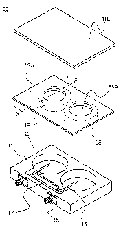
As shown in FIG. 1, a dielectric filter 10 comprises a case 11 made of an
iron body plated with silver for example, dielectric resonators 12, an ground
plate 13a, coupling probes 14, and external connectors 15 attached to the
outer
wall of the case 11 and connected to the probes 14, respectively.
Thin film multilayered electrodes 30 each composed of conductive layers
CA 02260644 1999-02-03
- 6 -
and dielectric layers laminated to each other and formed by sputtering and the
like are provided on the two opposite sides of each dielectric resonator 12,
respectively. The ground plate 13a is preferably made of an alloy of iron and
nickel, so that the coefficient of linear expansion of the dielectric
resonators 12
can be made substantially equal to that of the ground plate 13a. This prevents
the dielectric resonators 12 and the ground plate 13a from being cracked
between them, due to changes in temperature. Each coupling probe 14 is a
metallic wire. One end of the probe 14 is connected to the center conductor of
the external connectors 15. The probe 14 is elongated in the space between
1 o the dielectric resonator 12 and the case 11. A signal transmitted from the
external connector 15 arrives at the probe 14. The probe 14 and the dielectric
resonator 12 are capacitively coupled. The dielectric resonator 12 may have a
prism shape. The case 11 may be a ceramic case provided with a metallic
conductive layer formed on thereon.
Hereinafter, joining of the dielectric resonator 12 to the ground plate 13
will be described with reference to FIG. 2.
The ground plate 13a is provided with a protuberant portion 40a having
an under side with a smaller area than the upper side of the dielectric
resonator
12, formed by press working and the like, as shown in FIG. 2. Preferably, the
under side of the protuberant portion is substantially flat. A creamy solder
20 is
made to adhere mainly to the under side of the protuberant portion 40a of the
ground plate 13a, as shown in FIG. 2. The dielectric resonator 12 is fixed in
such a manner that the upper side of the resonator 12 is made adjacent to the
protuberant portion 40a, and the solder is heated. On this occasion,
preferably,
the side edge of the thin film multilayered electrode 30 formed in the
dielectric
CA 02260644 1999-02-03
_ 'j _
resonator 12 avoids to be positioned under the side edge of the protuberant
portion 40a of the ground plate 13a. This is because the solder coated onto
the
under side of the protuberant portion is prevented from reaching the side edge
of
the thin film multilayered electrode. In other words, it is preferable that
the
protuberant portion is as distant as possible from any point of the side edge
on
the upper side of the dielectric resonator. In other words, the side edge of
the
electrode is as distance as possible from the circumference of the top of the
protrude.
In such a manner, a space is provided between the side edge of the thin
l0 film multilayered electrode 30 and ground plate 13a. When the solder 20 is
permeated between the thin film multilayered electrode 30, the ground plate
13a
functions as a buffer for the solder 20. Thus, the solder 20 is prevented from
reaching the side edge of the thin film multilayered electrode 30. The
protuberant portion may have an optional shape. Desirably, the height of the
protuberant portion is constant so that a solder film uniform in thickness can
be
formed between the resonator and the protuberant portion.
The protuberant portion 40a of the ground plate 13a is joined to the thin
film multilayered electrode 30 through the surface portion thereof which is
smaller than the range on the upper side of the thin film multilayered
electrode
30 defined by the side edge. Accordingly, even if a stress, caused by
vibration
and impact, is applied to the ground plate 13a, the range where the force
exerts
a main influence lies on the inner side of the side edge of the thin film
multilayered electrode 30. Therefore, the stress applied to the side edge of
the
thin film multilayered electrode 30, which is ready to be peeled, is feeble.
Thus,
there is no possibility that the thin film multilayered electrode 30 is peeled
due to
CA 02260644 1999-02-03
_ g _
an external vibration or impact.
The ground plate 13a soldered to be fixed to the dielectric resonator 12 is
sandwiched between the trunk 11 a and the lid 11 b of the case 11, namely, it
is
disposed inside of the case 11.
According to a second embodiment of the present invention, an aperture
is provided for a part of the protuberant portion of the ground plate. The
configuration in the instant embodiment is the same as that of the first
embodiment except for the aperture. FIG. 3 is a perspective view of the
dielectric resonator and the ground plate. FIG. 4 is a cross-sectional view
l0 along a line Y - Y of FIG. 3.
In the instant embodiment, a circular hole 41 b is so provided for the
protuberant portion 40b by punching and the like, as to have a size smaller
than
the range of the protuberant portion 40b defined by the side edge thereof.
Hereinafter, a process of soldering the dielectric resonator 12 provided
with the thin film multilayered electrode 30 thereon to the ground plate 13b
formed as described above will be now described. The dielectric resonators 12
and the protuberant portion 40b are arranged in their preferred positions
relative
to each other as described above. A solder is cast to lie between the
dielectric
resonator 12 and the protuberant portion 40b by contacting a solder iron from
the side A shown in FIG. 4 through the hole 41b to the upper side of the thin
film
multilayered electrode 30. The amount of the cast solder is such that it
sufficiently extends between the protuberant portion 40b and the upper side of
the resonator. Preferably, the amount of the solder is such that the surface
of
the liquid solder reaches the side wall of the protuberant portion 40b,
depicting a
smooth curved surface. When such an amount of the solder is cast, it does not
CA 02260644 1999-02-03
_ g _
reach the side edge of the thin film multilayered electrode.
Accordingly, the protuberant portion 40b of the ground plate 13b is joined
to the thin film multilayered electrode 30 through the surface portion thereof
which is smaller than the range on the upper side of the thin film
multilayered
electrode 30 defined by the side edge. Accordingly, even if a stress, caused
by
vibration and impact, is applied to the ground plate 13a, the range where the
force exerts a main influence lies on the inner side of the side edge of the
thin
film multilayered electrode 30. Therefore, the stress applied to the side edge
of
the thin film multilayered electrode 30, which is ready to be peeled, is
feeble.
l0 Thus, there is no possibility that the thin film multilayered electrode 30
is peeled
due to an external vibration or impact.
With the hole 41 b provided for the ground plate 13b, soldering can be
carried out by operating a solder iron and the like from the side A of the
ground
plate 13b. Accordingly, the work is simplified.
Moreover, a third embodiment of the resent invention will be now
described. The arrangement and function of the dielectric filter in the
instant
embodiment are the same as those in the second embodiment. Their
description will be omitted, and only joinining of the dielectric resonator to
the
ground plate will be explained in reference to FIGS. 5 and 6. FIG. 5 is a
2o perspective view of the dielectric resonator and the ground plate. FIG. 6
is a
cross-sectional view along a line Z - Z of FIG. 5.
In the instant embodiment, the columnar thin film multilayered electrodes
30 are formed by sputtering on the opposite sides of the dielectric resonator
12.
A protubernat portion 40c is formed by press working. The protuberant portion
40c of the ground plate 13c made of an alloy of iron and nickel has the under
CA 02260644 1999-02-03
- 10 -
side of which the area is smaller than the upper side of the dielectric
resonator
12 in opposition to the protuberant portion. Preferably, the under side is
substantially flat. In the under side of the protuberant portion 40c, an
aperture
41 c is formed by punching.
At least one bay-shape portion is provided with the aperture on the
periphery thereof. The bay portion may have an optional shape and size on
condition that the area where the solder and the aperture are contacted with
each other is increased.
As described above, the aperture 41 c of the ground plate 13c, if it is so
l0 shaped as to have a cut 42, has a circumferential length, where the
soldering is
carried out, longer than that of the aperture having a shape excluding the cut
42.
Accordingly, this assures the joining by soldering of the dielectric resonator
and
the protuberant portion.
A dielectric duplexer according to an embodiment of the present invention
will be described below with reference to FIG. 7. FIG. 7 is an exploded
perspective view of the dielectric duplexer of this embodiment. In this
embodiment, like parts to those in the first embodiment are designated by like
reference numerals, and the detailed description of the parts will be omitted.
As shown in FIG. 7, a dielectric duplexer 50 of this embodiment includes
2o a first dielectric filter portion 60a made up of two columnar dielectric
resonators
12a, and a second dielectric filter portion 60b made up of two columnar
dielectric
resonators 12b, which are disposed in a case 5. On the two opposite sides of
the respective dielectric resonators 12a and 12b, the thin film multilayered
electrodes each composed of conductive layers and dielectric layers laminated
together are formed, respectively. The two dielectric resonators 12a
CA 02260644 1999-02-03
- 11 -
constituting the first dielectric filter portion 60a are coupled through a
capacitance produced by a coupling member 16a and functions as a transmitting
band pass filter. The two dielectric resonators 12b constituting the second
dielectric filter portion 60a and having a resonant frequency different from
that of
the dielectric resonators 12a of the first dielectric filter 60a are also
coupled
together through a capacitance produced by a coupling member 16b, and
functions as a receiving band pass filter. An electric probes 14a as an
external
connecting means connected to the dielectric resonators 12a of the first
dielectric filter portion 60a is connected to an external connector 15a so
that it is
l0 connected to an external transmitting circuit. An electric probe 14b
connected
to the dielectric resonator 12b of the second dielectric filter portion 60b is
connected to an external connector 15b, so that it is connected to an external
receiving circuit. Further, an electric probe 14c connected to the dielectric
resonator 12a of the first dielectric filter portion 60a and an electric probe
14d
connected to the dielectric resonator 12b of the second dielectric filter
portion
60b are connected to an external connector 15c, so that they are connected to
an external antenna.
The dielectric duplexer having the above-described configuration
functions as a band pass dielectric filter. That is, the first dielectric
filter portion
60a allows a wave with a predetermined frequency to pass, and the second
dielectric filter portion 60b does a wave with a different frequency from that
of
the above wave to pass.
In the instant embodiment, the dielectric resonators 12a and 12b are
soldered to the ground plate 13d and sandwiched between the trunk 51 b of a
shielding cavity 51 and a lid 51 b to be disposed inside of the case 51. For
the
CA 02260644 1999-02-03
- 12 -
ground plate 13d, the protuberant portions 40c and the holes 41 c for
soldering
are provided. Each of them has an area under side thereof which is smaller
than that of on the upper side of the thin film multilayered electrode,
defined by
the side edge thereof. This prevents the solder from reaching the side edge of
the thin film multilayered electrode. That is, the thin film multilayered
electrode
is prevented from being short-circuited. Thus, the dielectric duplexer having
a
high non-load Q can be provided. In addition, there is reduced the possibility
that the thin film multilayered electrode is peeled by an external impact and
the
like.
1 o Moreover, a communication device according to an embodiment of the
present invention will be described below with respect to FIG. 8. FIG. 8 is a
schematic diagram of a communication device of this embodiment.
As shown in FIG. 8, a communication device 70 of this embodiment
comprises a the dielectric duplexer 50, a transmitting circuit 71, a receiving
circuit 72, and an antenna 73. In this case, the dielectric duplexer 50 is the
same as described in the above embodiment. The external connector 15a
connected to the first dielectric filter portion 60a, shown in FIG. 7 is, is
connected to the transmitting circuit 71. The external connector 15b connected
to the second dielectric filter portion 60 b is connected to the receiving
circuit 72.
In addition, the external connector 15c is connected to an antenna 73.
In the instant embodiment, the dielectric resonators are soldered to the
ground plate and sandwiched between the trunk of the case and an external,
that is, it is disposed inside of the case. For the ground plate, the
protuberant
portions and the holes for soldering are provided. Each of them has an area
under side thereof which is smaller than that of on the upper side of the thin
CA 02260644 1999-02-03
- 13 -
film multilayered electrode, defined by the side edge thereof. Accordingly,
the
solder is prevented from reaching the side edge pf the thin film multilayered
electrode. That is, the thin film multilayered electrode is prevented from
being
short-circuited. Thus, the communication device having a high non-load Q can
be provided. In addition, there is reduced the possibility that the thin film
multilayered electrode is prevented by an external impact and the like. Thus,
the communication device having a high reliability can be obtained.