Note: Descriptions are shown in the official language in which they were submitted.
CA 02261188 2001-02-O1
1
PHASE SHIFTER NETWORK FOR ANTENNA ARRAY
This invention relates to antennas and in particular to an arrangement to
electrically down-tilt the electromagnetic wave pattern associated with a
transmit
antenna array, or electrically re-orient a receive antenna array.
It is sometimes desirable to adjust the orientation of the electromagnetic
wave
pattern of a transmit antenna array, particularly a downward adjustment,
typically 0°
to 15° below horizontal, when the antenna is located at a higher
altitude than other
antennas that communicate with the transmit antenna array. The downward
1o adjustment of the radiation pattern alters the coverage area and may
enhance
communication with mobile users situated in shadowed areas below the transmit
antenna array.
Besides actually mechanically tilting the entire antenna assembly, it is known
to
electrically down tilt the radiation pattern by controllably varying the
relative phases
between two or more radiating elements of the antenna array.
One known method by which the relative phase between two or more radiating
elements can be changed is to change the relative lengths of respective
transmission
lines connecting the antenna's common feed point to each element of the
antenna
array. Typically, various predetermined lengths of jumper cable are provided
which
20 are selectively connected between the common feed and each element to
obtain a
desired down-tilt. The jumper cables include co-axial connectors to facilitate
connection. Furthermore, if stripline is used to conneca the common feed point
to the
respective elements of the antenna array, some form of transition means is
required to
couple the jumper cable's co-axial connections to the strip line. A
disadvantage of this
known method is that it is relatively expensive, less reliable and susceptible
to the
generation of intermodulation products.
Another known method by which the relative phase between two or more
radiating elements can be changed is to change the propagation velocity of the
transmission line connecting the common feed point to at (east some of the
elements
30 of the antenna array. Typically, this latter method is achieved by
selectively changing
the dielectric constant of the transmission line dielectric:. If the
transmission line is in
CA 02261188 2001-02-O1
la
the form of a conductive strip, the propagation velocity thereof is changed by
introducing a dielectric material between the strip and its associated ground
plane.
It is, however, well understood that the introduction of dielectric material
under
CA 02261188 2001-02-O1
2
such a conductive strip causes the strip's normal impedance to be disturbed.
For
example, if a conductive strip having a certain width is spaced above a ground-
plane
at a certain distance such as to present a 50 ohm impedance, the introduction
of
dielectric material between the conductive strip and the ground-plane will
reduce the
value of this impedance to a value that depends upon the effective dielectric
constant
of the dielectric material. The resulting impedance mismatch would cause a
degradation of return-loss performance of the antenna array.
Australian Patent No. 664625 discloses an arrangement of an adjustable
phase shifter comprising dielectric phase shifter elements moveably interposed
to between conductive strips that couple radiating elements, and a common
ground
plane. The phase shifter elements are of a characteristic configuration which
avoids
disturbing the normal impedance during adjustment. This known arrangement,
however, requires that respective phase shifter elements be located between
each
active strip line and the conductive ground plane. Such an arrangement imposes
constructional disadvantages as well as limitations to the range of phase
shift
produced, which consequently imposes limits to the range of tilt.
It is an object of the present invention to provide an adjustable phase
shifter
arrangement of improved simplicity and compactness.
It is a further object of the present invention to provide an adjustable phase-
20 shifter arrangement which allows a single phase-shifter element of
relatively small
dimensions to adjust the electrical beam tilt of a multi-element antenna array
in a
simple manner.
It is still a further object of the invention to provide a phase-shifter
arrangement
which allows a relatively wide range of phase shift.
According to the present invention, there is
provided a phase shifter element comprising a substantially
planar conductor arranged to provide at least one signal
path, the at least one signal path including a signal input
at one end thereof, a signal output at the other end
30 thereof and an intermediate section of conductor having at
least one portion extending substantially in a first
CA 02261188 2001-02-O1
3
direction, said planar conductor being supported in a
substantially parallel relationship with a conductive
ground plane member, wherein said phase shifter element
further includes a planar dielectric member adjacent said
conductor such that the conductor i_s between the planar
dielectric member and the ground plane, and a variable
adjustment means arranged to selectively produce relative
movement between the conductor and the planar dielectric
member in a direction which is substantially transverse to
said first direction of said intermediate section of the
conductor, the phase of a signal at the signal output being
determined by the extent to which the planar dielectric
member overlaps said planar conductor, such overlap being
varied by said relative movement;
wherein at least one of said portion of said
intermediate conductor and planar dielectric member having
an edge with a plurality of projections extending in a
direction parallel to the direction of said relative
movement, such that an amount of overlap between the
conductor and the planar dielectric member is segmented.
According to the present invention, there is also
provided a phase shifter element comprising a transmission
line provided by a planar first dielectric member having a
first surface opposite a second surface, said first surface
supporting thereon a pattern of at least one conductive
track arranged to provide a signal path of a predetermined
physical length, the at least one conductive track
including a signal input at one end thereof, a signal
output at the other end thereof and an intermediate section
of conductive track having at least one portion extending
substantially in a first direction, said transmission line
CA 02261188 2001-02-O1
4
being supported in a substantially parallel relationship
with a conductive ground plane member, said ground plane
member being either spaced from or contiguous with said
dielectric member's second surface, wherein said phase
shifter element further includes a second planar dielectric
member adjacent said first surface of said first dielectric
member, and variable adjustment means arranged to
selectively produce relative movement between the first and
second dielectric members in a direction which is
substantially transverse to said first direction of said
intermediate section of conductive track, the phase of a
signal at the signal output being det=ermined by the extent
to which said second dielectric member overlaps said
pattern of said at least one conductive track, such overlap
being varied by said relative movement.;
wherein at least one of .said portion of said
conductive track and said second dielectric member having
an edge with a plurality of projections extending in a
direction parallel to the direction of said relative
movement, such that an amount of overlap between the at
least one conductive track and the second dielectric member
is segmented.
According to the present invention, there is also
provided a phase shifter element comprising a transmission
line provided by a planar first dielectric member having a
first surface opposite a second surface, said first surface
supporting thereon a pattern of at least one conductive
track arranged to provide a signal path of a predetermined
physical length, the at least one conductive track
including a signal input at one end thereof, a signal
CA 02261188 2001-02-O1
4a
output at the other end thereof and an intermediate section
of conductive track having at least one portion extending
substantially in a first direction, raid transmission line
being supported in a substantially parallel relationship
with a conductive ground plane member, said ground plane
member being either spaced from or contiguous with said
dielectric member's second surface, wherein said phase
shifter element further includes a se~~ond planar dielectric
member adjacent said first surface of said first dielectric
l0 member, said second planar dielectric member including at
least two opposite edges, and variable adjustment means
arranged to selectively produce rel<~tive linear movement
between the first and second dielectric members in a
direction which is substantially transverse to said first
direction of said intermediate section of conductive track,
the phase of a signal at the respective signal output being
determined by the extent to which said second dielectric
member overlaps said pattern of said at least one
conductive track, such overlap being varied by said
20 relative linear movement;
wherein at least one of said portion of said at
least one conductive track and said second dielectric
member having an edge with a plurality of projections
extending in a direction parallel to the direction of said
relative movement, such that an amount of overlap between
the at least one conductive track and the second dielectric
member is segmented.
Preferably, the variable adjustment means comprises an arrangement of said
second planar dielectric member slidably fixed adjacent said first surface of
said first
3 0 planar dielectric member , the phase of a signal at the or each said
signal output
means being determined by the extent to which said second planar dielectric
member
CA 02261188 2001-02-O1
4b
overlaps said pattern of said conductive tracks) , such overlap extent being
varied by
linear movement of said second planar dielectric member .
In order that the invention may be readily carried into effect, an embodiment
thereof will now be described in relation to figures of the accompanying
drawings, in
which:
Figure 1 is a top view of a first embodiment of the phase-shifter arrangement
of
the present invention.
Figure 2 is a top view of a printed circuit board (PCB), distribution element
incorporated in the phase-shifter arrangement shown in Figure 1.
1 o Figure 3 is a side view of the phase-shifter arrangement shown in Figure
1.
Figure 4 is a schematic layout of an antenna array incorporating the phase-
shifter shown in Figure 1.
Figure 5 shows a top view of a second embodiment of the phase-shifter
arrangement of the present invention.
Figure b shows a top view of a PCB element incorporated in the phase-shifter
arrangement shown in Figure 5.
Figure 7 is a schematic layout of an antenna array incorporating the phase-
shifter arrangement shown in Figure 5.
Figure 8 is a top view of a third embodiment of the phase-shifter arrangement
.. CA 02261188 1999-02-18
of the present invention.
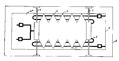
Referring to Figures 1 - 4 of the drawings, there is shown a PCB distribution
element (A) comprising a planar dielectric circuit board (2) supporting a
pattern of
conductive tracks (3) on a first surface 2a thereof. The conductive tracks and
the
5 dielectric circuit board form a transmission line network for splitting a
signal applied to
a signal input terminal (I) into three paths that terminate respectively in
three terminals
(T, B and C) for feeding the input signal to the Top (T), Bottom (B) and
Centre (C)
sections of an antenna array (see Figure 4). The distribution element (A) is
supported
in a spaced relationship with a conductive ground plane (B); the planar
dielectric
circuit board's (2) second surface (2b) and the ground plane facing one
another.
Alternately, the second surface (2b) of the said circuit board and the ground
plane can be contiguous (not shown).
A moveable planar dielectric element (C) having a series of teeth (4,5) along
opposite edges, is slidably mounted and adjacent to the top surface of the
distribution
element (A). The moveable dielectric element (C) is supported in a linear
slidable
manner by two parallel rods (6,7) attached to the ground plane (B). It will be
understood that a rotational arrangement of a dielectric element could be
adapted,
and is envisaged.
By selectively moving the dielectric element, the phases in the top and bottom
sections of the antenna array are changed in opposite directions so that the
phase in
one section is increased and in the other section is decreased, which causes
the
radiating beam to tilt.
Referring to Figures 5 - 7 of the drawings there is shown a second embodiment
of the invention for use with a two section antenna array (Fig.7). The phase-
shifter
arrangement of this embodiment is similar to the one described in relation to
Figures 1
- 4, except that only a single elongated, serpentine conductive track 3a is
provided to
form a transmission line whose distal ends terminate at respective terminals T
and B.
A moveable dielectric element C1 is in the form of a bisected dielectric
element shown
in Figure 1. It will be understood that a rotational arrangement of the
dielectric
element could be adapted for the arrangement shown in Figure 5.
Referring to Figure 8, there is shown an embodiment which, instead of using a
series of teeth along edges of the movable planar dielectric element (C1 ), as
shown,
CA 02261188 1999-02-18
6
for example, in Figure 5, an electrically equivalent configuration is used.
This is
achieved by providing the conductive tracks 3 with a non-linear portion in the
form of
a meandering pattern 8 of a triangular configuration. Other configurations,
such as,
for example, trapezoid or semi-ellipsoid could be adapted. In the embodiment
shown
in Figure 8, the movable dielectric element C1 is provided with a straight
edge 9.