Note: Descriptions are shown in the official language in which they were submitted.
CA 02261970 1999-02-16
VERTICAL SPARK GAP FOR
MICROELECTRONIC CIRCUITS
The present invention is directed to an arrangement to alleviate the
deleterious
effects of electrostatic discharges in electronic circuits and more
particularly, the
present invention is directed to a vertical spark gap suitable for use in
microelectronic
circuits.
Spark gaps have been proposed earlier in the art with the objective of
counteracting electrostatic discharges on integrated circuits. Previous
arrangements
employed aluminum, however, due to the physical properties of the metal and
especially its low melting point resulted in mass transport through and across
the oxides
and dielectrics and this was found to be problematic thus making aluminum an
impractical choice.
Another limitation encountered in this field relates to the control of the
breakdown voltage. Spark gaps are typically lateral and formed by
photoengraving
techniques. This process makes tolerances difficult to control leading to
problems in
forming short spark gaps.
Finally, limitations in successful operation of spark gaps in plastic packages
are
realized since the air in the gap is displaced by the plastic.
One aspect of one embodiment of the present invention is to provide a spark
gap assembly suitable for use in electronic circuits, comprising:
a first at least partially conductive layer;
a second at least partially conductive layer;
nonconductive material positioned between the first layer and the second layer
maintaining a vertically spaced relationship therebetween;
at least one opening in at least one of the first layer and the second layer,
the
nonconductive material removed from the layer having the at least one opening,
whereby a vertical gap is formed between and communicates with each layer.
A further aspect of one embodiment of the present invention is to provide a
spark gap assembly, comprising:
a first at least partially conductive layer;
a second at least partially conductive layer;
CA 02261970 1999-02-16
2
nonconductive material positioned between the first layer and the second layer
maintaining a vertically spaced relationship therebetween, each layer in an
overlying
relationship with the material; and,
at least one opening in at least one of the first layer and the second layer,
the
nonconductive material removed from the layer having the at least one opening,
the
opening comprising a vertical spark gap for dissipating electrostatic charge.
As a further aspect of one embodiment of the present invention, there is
provided a method of forming a vertical spark gap suitable for use in
dissipating
electrostatic buildup in an integrated circuit, comprising:
providing a first at least partially conductive layer and a second at least
partially
conductive layer;
positioning nonconductive material between the first layer and the second
layer
maintaining a vertically spaced relationship therebetween; and
forming at least one opening in one of the first or the second layer by
etching
insulating material associated with the first layer and the second layer to
form a vertical
gap therebetween.
Having thus described the invention, reference will now be made to the
accompanying drawings illustrating preferred embodiments and in which:
Figure 1 is a plan view of a spark gap arrangement of the prior art;
Figure 2a is a cross-section of an integrated circuit;
Figure 2b is an end elevation view of Figure 2a;
Figure 3a is a plan view of a first embodiment of the present invention;
Figure 3b is a side view of Figure 3a;
Figure 4a is a plan view of a second embodiment of the present invention;
Figure 4b is a cross-section of Figure 4a;
CA 02261970 1999-02-16
3
Figure 5 is a plan view of a further embodiment of the present invention;
Figure 6a is a top plan view of a further embodiment of the present invention;
Figure 6b is a cross-section of Figure 6a;
Figure 7a is a top plan view of yet another embodiment of the present
invention
where a spark gap structure is shown to incorporate a metal to N+ arrangement;
Figure 7b is a top plan view of yet another embodiment of the present
invention
where a spark gap structure is shown to incorporate a different metal to N+
arrangement;
Figure 7c is a top plan view of the arrangement includes two conductive
metals;
Figure 7d is the arrangement includes a metal to a poly;
Figure 7e is the arrangement includes a metal to gate poly;
Figure 7f is a further metal to poly;
Figure 7g is a gate poly to N-substrate;
Figure 7h is a poly to an N-substrate;
Figure 7i is a metal to a gate poly; and
Figure 7j is poly to a P-Well.
Similar numerals employed in the text denote similar elements.
Referring now to the drawings, Figure 1 illustrates a typical lateral spark
gap
assembly, globally denoted by numeral 10 in which strips of metal 12 and 14
are placed
in close proximity and suitable for connection to nodal points in a circuit
(not shown) to
be protected by the gap. The gap is generally designated by numeral 16.
CA 02261970 1999-02-16
4
Figure 2a illustrates a cross-section of a typical integrated circuit having a
passivation layer 18, a metal layer 20, dielectric layer 22, a first level
metal layer 24, a
pyroglass layer 26, a second level poly silicon layer 28, a capacitor oxide
layer 30, a
first level poly silicon layer 32, a thermal oxide layer 34, a diffusion layer
36 and a
substrate layer 38. With reference to Figure 2b, implementation of a vertical
spark gap
involves a lateral component broadly denoted by numeral 40 and this introduces
alignment errors.
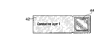
This problem has been alleviated by the invention and with reference now to
Figure 3a, shown is a conductor in a first layer 42 which surrounds and
overlies the
second conductor 44. This vertical arrangement avoids the alignment problem
set forth
with respect to Figure 2b. Figure 3b illustrates the arrangement in Figure 3a
in cross-
section for greater detail and illustrates the vertical spark gap 46 formed
between
conductive layer 42 and conductive layer 44. In each case, the conductive
layers 42
and 44 have an insulating material 48 positioned therebetween and by etching
(to be
discussed in greater detail hereinafter), the insulator material around the
opening
between the two layers can be removed to create an open gap between the two
layers
42 and 44.
Figure 4a illustrates a further embodiment of the invention in which
conductive
layer 44 includes an opening 50. The insulator material 48 is removed about
hole 50
thus providing the vertical air gap shown more clearly in the cross-section of
Figure 4b.
In this manner, the air gap 50 is formed between the underside of the hole 50
and the
lower plate and conductive layer 44. It will be apparent to those skilled that
this
arrangement could easily be reversed. This structure provides a vertical spark
gap with
advantage of providing a well controlled, and if required, extremely small air
gap which
may be of the order of nanometers. The thickness of the insulating layer 48
can be
used to set the spark gap voltage depending upon the intended use for the
spark gap.
The opening 50 is used to expose the underlying insulator to a process for
removing the
insulator from the region of the hole 50 to form an air gap between the two
conductors
42 and 44. Suitable methods such as etching or other known procedures can be
employed to effect this result. The opening 50 can also serve to exclude
packaging
material from the gap if it is made narrow enough (<1 gym).
CA 02261970 1999-02-16
As an alternative, as illustrated in Figure 5, in the context of an integrated
circuit
(not shown), the bottom plate could be a first level of metal 52 separated
from a second
layer of metal 54 by dielectric 56 shown in chain line. Double dielectrics
will be readily
apparent to those skilled in the art. In this arrangement, the spark gap or
opening,
represented by numeral 58, is in the form of a narrow slot.
Many implementations are possible and the one selected will depend upon the
application intended with the primary factor being the vertical spark gap
dimension. In,
for example, high voltage discharge applications in a plastic package,
reference will be
made to Figure 6a and 6b. In the embodiment shown, the arrangement includes a
poly
silicon layer 58 having a narrow slot 60 grayed through it to the underlying
oxide,
generally denoted by numeral 62 and comprising the second conductive layer in
this
example. The arrangement is exposed to etchant to remove insulation material
64
between the slot 60 of membrane 58 and layer 62 to thus form the spark gap 66.
In an
electrostatic discharge, an electric field is developed between the periphery
of the slot
60 and the lower plate 64. Avalanche or dielectric breakdown of the gas in the
spark
gap 66 will occur (depending upon the spark gap dimension) leading to a low
electric
discharge between plates 58 and 62. The breakdown voltage is made lower than
the
damage threshold of the component to be protected (not shown), no damage to
the
circuit will result. Either or both of the plates 58, 62 can be designed to
limit the energy
dissipated in the spark gap region 66.
It has been found that a vertical spark gap can be constructed between any two
conductive or semi-conductive layers on an integrated circuit. The
availability of
conductive layers and the spacings will vary from process to process. Figures
7a
through 7j show alternative examples for the use of double metal, double poly
silicon
integrated circuit processes. In the embodiments of 7a through 7j, the
conductive layer
is represented by numeral 52, conductive layer 2 is represented by numeral 54,
the
spark gap by numeral 66, the N+ active represented by numeral 70, the cap poly
silicon
by numeral 72, the gate poly silicon by numeral 74, the contact points by
numeral 76,
the P+ active by numeral 78, the N-Well by numeral 80, and the P-Well by
numeral 82.
Suitable materials which can be employed for the spark gap assembly according
to the present invention can include the refractory metals and single crystal
silicon, poly
silicon and high melting point alloys.
CA 02261970 1999-02-16
6
An important feature in this invention is that by making the slot in the top
conductor small enough, plastic material can be excluded from the gap thereby
allowing
application to integrated circuits packaged in plastic.
A second extremely important feature is that these devices can be made with
very low parasitic capacitance thereby allowing applications to the radio
frequency
market where input protection has, to date, not been feasible.
Applications are also possible in micro mechanical devices where junction
diodes are, typically, not present.
The invention can be applied to any variation of an integrated circuit as set
forth
herein previously and is particularly well suited for materials that are most
suited for
high voltage applications such as silicon carbide and diamond, both of which
have large
band gaps and high thermal conductivities.
In view of the fact that extremely short spark gaps are possible according to
the
present invention, the electrostatic discharge will be due to gas dielectric
breakdown
within the gap rather than by avalanche breakdown. Accordingly, this will
extend the
breakdown voltage to the range of values previously realized by making use of
junction
diodes. The energy dissipated in these low voltage discharges will be low
enough to
permit a very small spark gap device to be used.
Although embodiments of the invention have been described above, it is not
limited thereto and it will be apparent to those skilled in the art that
numerous
modifications form part of the present invention insofar as they do not depart
from the
spirit, nature and scope of the claimed and described invention.